
1
MSM9554/MSM9555
° Semiconductor
GENERAL DESCRIPTION
The MSM9554 and MSM9555 are LSI devices which demodulate FM character multiplex signals in
the DARC (DAta Radio Channel)
*1
format to acquire digital data. The MSM9554 and MSM9555
operate on 5V and 3V, respectively. In the DARC format, baseband signals at ordinary FM
broadcasting frequencies are multiplexed with 16k-bps digital data which are L-MSK-modulated at
76kHz.
Each of the MSM9554 and MSM9555 has a bandpass filter consisting of SCF, frame synchroniza-
tion circuit, and error correction circuit, on a single chip.
So, a system for acquisition of digital data can be easily constructed by externally mounting an FM
receiver tuner, microcontroller for control, and memory for temporary storage of data.
The MSM9554 and MSM9555 have a simple configuration, and are equipped with only necessary
functions. By making changes to software for the external microcontroller, the MSM9554 and
MSM9555 can meet the various requirements of FM multiplex broadcasting services which will be
offered in future.
These devices are best suited to the car radios and car navigation systems supporting VICSs (Vehicle
Information and Communication System)
*2
that have been serviced since Aprit, 1996.
*1 DARC is a registered trademark of NHK ENGINEERING SERVICES, INC.
Note that a contract needs to be made with NHK Engineering Service if a manufacturer produces/
sells electronic equipment utilizing the DARC technology.
*2 If samples or detail documents are to be provided, contracts with VICS center are reqired
beforehand.
FEATURES
∑ Built-in discrambler supporting VICS
∑ Pin compatible with MSM9552/MSM9553
∑ Built-in bandpass filter (SCF)
∑ Built-in timer internal to block
∑ Built-in block synchronization circuit and frame synchronization circuit
∑ Setting of the number of synchronization protecting stages
∑ Regeneration of data clocks by digital PLL
∑ 1T delay detection
∑ Built-in error correction circuit
∑ Built-in layer 4 and layer 2 CRC check circuit
∑ Microcontroller parallel interface
∑ Clock output for external devices (64kHz to 8.192MHz selectable)
∑ International standard frame format
∑ Power source:
5V (MSM9554), 3V (MSM9555)
∑ Package
44-pin plastic QFP (QFP44-P-910-0.80-2K) (Product name: MSM9554GS-2K/MSM9555GS-2K)
° Semiconductor
MSM9554/MSM9555
LSI Devices for FM Multiplex Data Demodulation
Preliminary
° Semiconductor
MSM9554/MSM9555
2
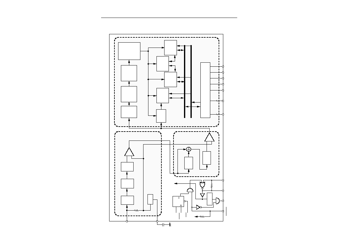
BLOCK DIAGRAM
A
IN
Data bus
DB0-DB7
Address
AD0-AD5
CS
WR
RD
CLR
+
≠
1T delay
circuit
LPF
Variable
gain
AMP
BPF
(SCF)
XTAL1
XTAL2
XOUT
XOUTC
D
Q
CK
DB2
WR31
CLR
DV
DD
Frequency
divider
LSI internal
clock
Limitter
Vref
+
≠
Limitter
SG
LPF
Clock
regeneration
Block
synchronization
Frame
synchronization
Timing
control
PN
descrambler
34Byte RAM
•
2
Error
correction
&
Layer 2 CRC
VICS
descrambler
CPU interface
Data bus
Addressbus
INT
Filter
Delay Detection
Digital Signal
Processor
Layer 4 CRC

3
MSM9554/MSM9555
° Semiconductor
PIN CONFIGURATION (TOP VIEW)
34
44
33
23
22
12
1
11
A0
XOUT
CS
XTAL2
XTAL1
DV
DD
DGND
DB7
DB6
DB5
DB4
DB3
DB2
DB1
DB0
RD
NC
WR
INT
MOUT6
MOUT5
MOUT4
MON
ADETIN
AV
DD
AGND
SG
A
IN
XOUTC
MOUT0
MOUT1
MOUT2
MOUT3
A1
A2
A3
A4
A5
NC
CLR
IORD
IOWR
NC
NC
Note: Leave the NC pins open.
44-Pin Plastic QFP
° Semiconductor
MSM9554/MSM9555
4
PIN DESCRIPTION
Function
Pin
Type
Description
Micro-
controller
interface
16
I
Write signal to internal register
18
I
Read signal to internal register
15
O
Interrupt signal to microcontroller. "L": Occurrence of an
interrupt
31
I
Chip select signal.
"L": Read, write, and data bus signals valid
40
I
"L" initializes internal registers, and the device enters
power down mode
33 to 38
I
Address signal to internal register
19 to 26
I/O
Data bus signal to internal register
6
I
FM multiplex signal input
5
O
Analog reference voltage output pin. To prevent noise,
connect a capacitor between this pin and analog ground.
1
O
Analog section waveform monitor pin. The analog block is
specified by the analog control register.
2
I
Analog signal input pin for testing
41
42
I
Digital section test signal input pins. Internally pulled up.
8 to 14
O
Digital section test signal output and monitor output pins
29
I
8.192MHz crystal oscillator connection pin
30
O
8.192MHz crystal oscillator connection pin
32
O
Pin for supply of 64kHz to 8.192MHz clock to the outside
7
I
XOUT output control pin.
"L"=Clock output, "H"=Output disabled. Pulled up internally.
3
--
Analog section power supply pin
4
--
Analog ground pin
28
--
Digital section power supply pin
27
--
Digital ground pin
Tuner
interface
Analog
section test
Digital
section test
Clock
Power
supply
Symbol
WR
RD
INT
CS
CLR
A0 to A5
DB0 to DB7
A
IN
SG
MON
ADETIN
IORD
IOWR
MOUT0 to
MOUT6
XTAL1
XTAL2
XOUT
XOUTC
AV
DD
AGND
DV
DD
DGND

5
MSM9554/MSM9555
° Semiconductor
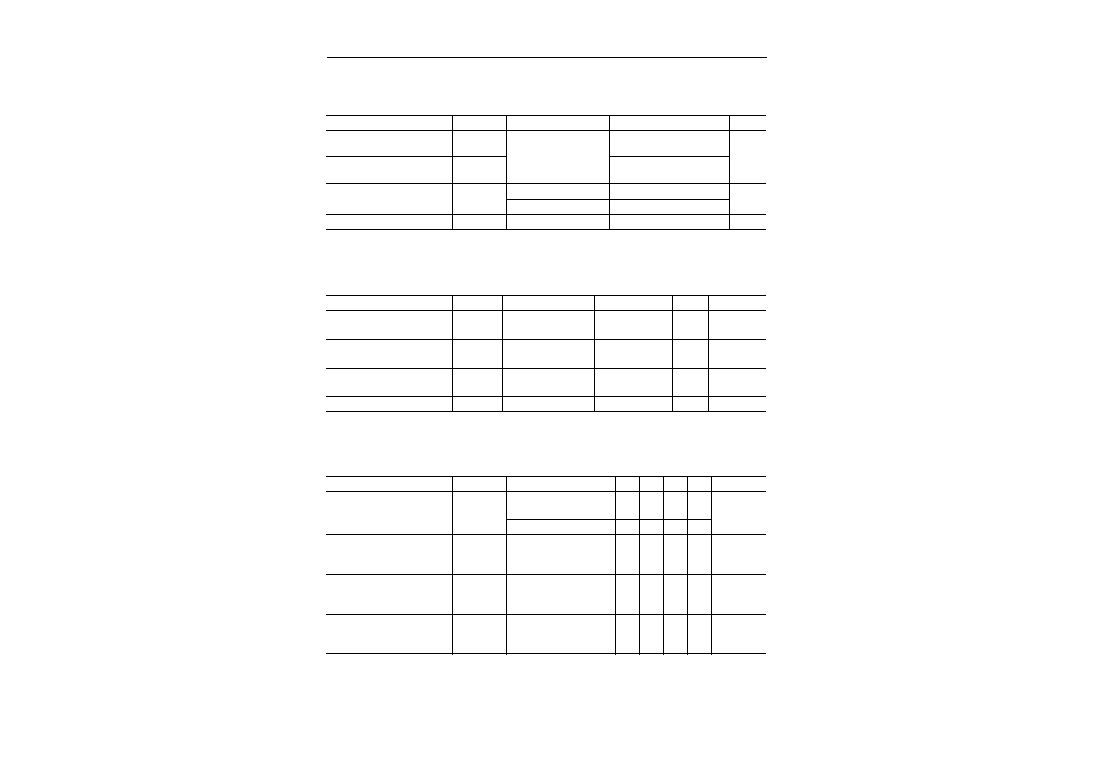
ABSOLUTE MAXIMUM RATINGS (MSM9554)
Parameter
Symbol
Condition
Rating
Unit
Power supply voltage
AV
DD
=DV
DD
Ta=25∞C
AV
DD
DV
DD
≠0.3 to +7.0
V
Input voltage
Output voltage
V
I
V
O
≠0.3 to AV
DD
+0.3
≠0.3 to DV
DD
+0.3
Maximum power dissipation
Ta=25∞C per package
P
D
400
mW
Ta=25∞C per output
50
Storage temperature
--
T
STG
≠55 to +150
∞C
RECOMMENDED OPERATING CONDITIONS (MSM9554)
Parameter
Symbol
Condition
Range
Unit
Power supply voltage
AV
DD
=DV
DD
AV
DD
DV
DD
4.5 to 5.5
V
Applied Pin
AV
DD
DV
DD
Crystal frequency
--
f
XTAL
8.192MHz ±100ppm
--
XTAL1
XTAL2
FM multiplex signal input
voltage
Composite signals,
including multiplex
signals
V
AIN
0.5 to 2
V
P-P
A
IN
Operating temperature
--
T
OP
≠40 to +85
∞C
--
ELECTRICAL CHARACTERISTICS (MSM9554)
Parameter
Symbol
Condition
Min.
Unit
Current consumption
During operation, No load
f=8.192MHz
I
DD
--
Applied Pin
AV
DD
DV
DD
Typ. Max.
18
34
mA
During power down, No load
--
--
20
mA
BPF pass band attenuation
72 - 80kHz
Variable gain amplifier
gain: 0dB
GAIN1
--
MON
--
3.0
dB
BPF reject band attenuation
0 - 53kHz
Variable gain amplifier
gain: 0dB
GAIN2
50
MON
--
--
dB
BPF reject band attenuation
100 - 500kHz
Variable gain amplifier
gain: 0dB
GAIN3
50
MON
--
--
dB
° Semiconductor
MSM9554/MSM9555
6
ABSOLUTE MAXIMUM RATINGS (MSM9555)
RECOMMENDED OPERATING CONDITIONS (MSM9555)
ELECTRICAL CHARACTERISTICS (MSM9555)
Parameter
Symbol
Condition
Rating
Unit
Power supply voltage
AV
DD
=DV
DD
Ta=25∞C
AV
DD
DV
DD
≠0.3 to +7.0
V
Input voltage
Output voltage
V
I
V
O
≠0.3 to AV
DD
+0.3
≠0.3 to DV
DD
+0.3
Maximum power dissipation
Ta=25∞C per package
P
D
400
mW
Ta=25∞C per output
50
Storage temperature
--
T
STG
≠55 to +150
∞C
Parameter
Symbol
Condition
Range
Unit
Power supply voltage
AV
DD
=DV
DD
AV
DD
DV
DD
2.7 to 3.3
V
Applied Pin
AV
DD
DV
DD
Crystal frequency
--
f
XTAL
8.192MHz ±100ppm
--
XTAL1
XTAL2
FM multiplex signal input
voltage
Composite signals,
including multiplex
signals
V
AIN
0.2 to 0.9
V
P-P
A
IN
Operating temperature
--
T
OP
≠20 to +75
∞C
--
Parameter
Symbol
Condition
MIN
Unit
Current consumption
During operation, No load
f=8.192MHz
I
DD
--
Applied Pin
AV
DD
DV
DD
TYP MAX
14
23
mA
During power down, No load
--
--
10
mA
BPF pass band attenuation
72 - 80kHz
Variable gain amplifier
gain: 0dB
GAIN1
--
MON
--
3.0
dB
BPF reject band attenuation
0 - 53kHz
Variable gain amplifier
gain: 0dB
GAIN2
50
MON
--
--
dB
BPF reject band attenuation
100 - 500kHz
Variable gain amplifier
gain: 0dB
GAIN3
50
MON
--
--
dB
(1)
(2)
7
MSM9554/MSM9555
° Semiconductor
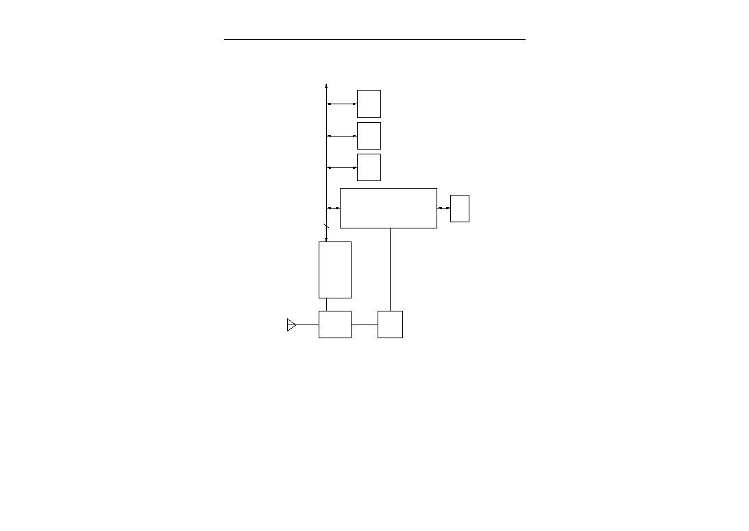
APPLICATION CIRCUIT
FM
tuner
FM multiplex
data demodulation
device
MSM9554 or MSM9555
8 bit
MCU
SRAM
Font
ROM
Display
PLL
Keys