
1/7
MSM9560
° Semiconductor
GENERAL DESCRIPTION
The MSM9560 is an IC which demodulates FM character multiplex signals in the DARC (Data Radio
Channel)
*1
format to obtain digital data. The MSM9560 operates at 4.5 to 5.5 V. In the DARC system,
16 kbps of digital data L-MSK modulated at 76 kHz is multiplexed on an ordinary FM broadcast base
band signal.
The MSM9560 contains on one chip a band pass filter using a switched capacitor filter (SCF) and a
group of circuits including a frame synchronization circuit and an error correction circuit.
By connecting an external FM receiver and memory for temporary data storage and by controlling
them by the CPU, a system for obtaining digital data can easily be constructed.
The FM multiplex demodulation ICs, the MSM9500-series devices, are configured with minimum
functions; so they will, merely by making changes to the software of the external microcomputer, be
able to respond flexibly to the many FM multiplex broadcast services that are going to come about
in the future.
The MSM9560 is best suited to radios and information processing devices that support DARC FM
multiplex broadcasting. It is also best suited to car radios and car navigation systems.
*1 DARC is a registered trademark of NHK Engineering Services.
Any manufacturer licensed by NHK Engineering Service can manufacture and sell products that
utilize the DARC technology.
For detailed information on license, please contact:
NHK Engineering Service
Phone: 81-3481-2650
FEATURES
∑ Pin compatible with MSM9552/MSM9553
∑ Built-in bandpass filter (SCF)
∑ Built-in block synchronization circuit and frame synchronization circuit
∑ Setting of the number of synchronization protection steps can be changed
∑ Data clocks are regenerated by digital PLL
∑ 1T delay detection
∑ Built-in vertical and horizontal error correction circuits
∑ Built-in layer 4 and layer 2 CRC processing circuit
∑ Parallel interface with microcontroller
∑ Clock output for external devices (64 kHz to 8.192 MHz variable)
∑ Compatible with the international standard frame format (ITU-R Rec. BS1194)
∑ Power supply:
4.5 to 5.5 V
∑ Package:
44-pin plastic QFP (QFP44-P-910-0.80-2K) (Product name: MSM9560GS-2K)
° Semiconductor
MSM9560
IC for FM Multiplex Data Demodulation
E2F0011-29-32
This version: Mar. 1999
Previous version: Jun. 1998
2/7
MSM9560
° Semiconductor
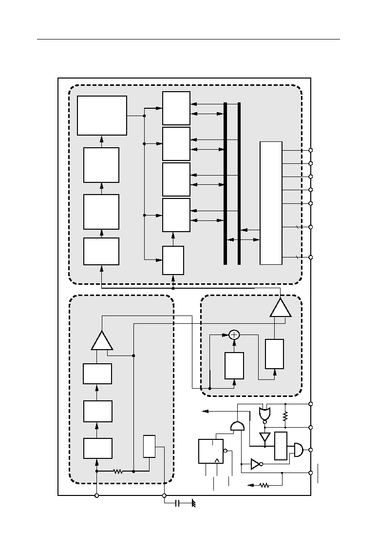
BLOCK DIAGRAM
AIN
Data bus
DB0-DB7
Address
AD0-AD5
CS
WR
RD
CLR
+
≠
1T delay
circuit
LPF
Variable
gain
AMP
BPF
(SCF)
XTAL1
XTAL2
XOUT
XOUTC
D
Q
CK
DB2
WR31
CLR
DV
DD
Frequency
divider
IC internal
clock
Limiter
Vref
+
≠
Limiter
SG
LPF
Clock
regeneration
Block
synchronization
Frame
synchronization
Timing
control
PN
Descrambler
34Byte RAM
•
2
Layer 4 CRC
CPU interface
Data bus
Address bus
INT
Filter Section
Delay Detection Section
Digital Signal
Processing Section
Error
correction
&
Layer 2 CRC
Read/Write
register

3/7
MSM9560
° Semiconductor
PIN CONFIGURATION (TOP VIEW)
NC : No-connection pin
44-Pin Plastic QFP
1
2
3
11
10
9
8
7
6
5
4
44
43
42
41
40
39
38
37
36
35
34
33
32
31
23
24
25
26
27
28
29
30
12
13
14
15
16
17
18
19
20
21
22
MOUT1
MOUT2
MOUT3
MON
ADETIN
AV
DD
AGND
XOUTC
MOUT0
MOUT5
MOUT6
INT
WR
NC
RD
DB0
DB1
DB3
NC
IOWR
IORD
A4
A3
A2
DB6
DB5
CS
XTAL2
DB7
AIN
A0
XOUT
DB4
SG
MOUT4
DB2
DGND
DV
DD
XTAL1
A1
A5
CLR
NC
NC
,
4/7
MSM9560
° Semiconductor
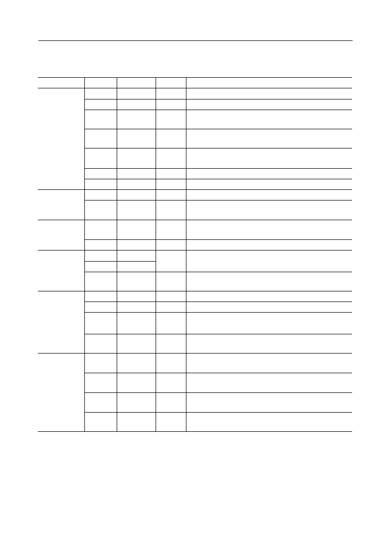
PIN DESCRIPTIONS
Function
Pin
Type
Description
Microcontroller
Interface
16
I
Write signal to internal register.
18
I
Read signal to internal register.
15
O
Interrupt signal to microcontroller. "L": An interrupt is
generated.
31
I
Chip select signal.
"L": Read, write, and data bus signals become active.
40
I
"L" : the internal registers are initialized and the device enters
power down mode.
33 to 38
I
Address signal to internal register.
19 to 26
I/O
Data bus signal to internal register.
6
I
FM multiplex signal input.
5
O
Analog reference voltage output pin. Connect a capacitor
between this pin and analog ground to prevent noise.
1
O
Analog section waveform monitoring pin. The analog block
mode setting is specified by the analog control register.
2
I
Analog signal input pin for testing.
41
I
Digital section test signal input pins. Internally pulled up.
8 to 14
O
Digital section test signal output and monitor output pins.
29
I
8.192 MHz crystal connection pin.
30
O
8.192 MHz crystal connection pin.
32
O
Pin for supply of 64 kHz to 8.192 MHz variable clock to the
outside.
7
I
XOUT output control pin.
"L" = Clock output, "H" = Output disabled. Pulled up internally.
3
--
Analog section power supply pin.
4
--
Analog ground pin.
28
--
Digital section power supply pin.
27
--
Digital ground pin.
Tuner
Interface
Analog
Section Test
Digital
Section Test
Clock
Power
Supply
Symbol
WR
RD
INT
CS
CLR
A0 to A5
DB0 to DB7
AIN
SG
MON
ADETIN
IORD
MOUT0 to
MOUT6
XTAL1
XTAL2
XOUT
XOUTC
AV
DD
AGND
DV
DD
DGND
42
IOWR

5/7
MSM9560
° Semiconductor
ABSOLUTE MAXIMUM RATINGS
RECOMMENDED OPERATING CONDITIONS
ELECTRICAL CHARACTERISTICS
Parameter
Symbol
Condition
Rating
Unit
Power Supply Voltage
AV
DD
= DV
DD
Ta = 25∞C
AV
DD
≠0.3 to +7.0
V
Input Voltage
V
I
≠0.3 to AV
DD
+ 0.3
Maximum Power Dissipation
Ta = 25∞C, per package
P
D
400
mW
Ta = 25∞C, per output
50
Storage Temperature
--
T
STG
≠55 to +150
∞C
DV
DD
V
O
≠0.3 to DV
DD
+ 0.3
Output Voltage
Parameter
Symbol
Condition
Range
Unit
Power Supply Voltage
AV
DD
= DV
DD
AV
DD
4.5 to 5.5
V
Applied Pin
AV
DD
Crystal Oscillation Frequency
--
f
XTAL
8.192 MHz ±100 ppm
--
XTAL1,
XTAL2
FM Multiplex Signal Input
Voltage
Composite signals
including multiplex
signals
V
AIN
0.5 to 2
V
P-P
AIN
Operating Temperature
--
T
op
≠40 to +85
∞C
--
DV
DD
DV
DD
Parameter
Symbol
Condition
Min.
Unit
Supply Current
When operating, no load
f = 8.192 MHz
I
DD
--
Applied Pin
AV
DD
,
DV
DD
Typ. Max.
14
28
mA
--
--
20
mA
BPF Pass Band Attenuation
72 to 80 kHz
Variable gain amplifier
gain: 0 dB
GAIN1
--
MON
--
3.0
dB
BPF Stop Band Attenuation
0 to 53 kHz
Variable gain amplifier
gain: 0 dB
GAIN2
50
MON
--
--
dB
BPF Stop Band Attenuation
100 to 500 kHz
Variable gain amplifier
gain: 0 dB
GAIN3
50
MON
--
--
dB
When in power down mode,
no load