
1/31
° Semiconductor
MSM9810
° Semiconductor
MSM9810
8-channel Mixing OKI ADPCM Type Voice Synthesis LSI
GENERAL DESCRIPTION
The MSM9810 is an 8-channel mixing voice synthesis IC, to which up to 128 Mbits of ROM and/
or EPROM storing voice data can directly be connected externally.
The device is straight 8-bit PCM playback, non-linear 8-bit PCM playback, 4-bit ADPCM
playback, and 4-bit ADPCM2 playback selectable and provides 2-channel stereo output and
volume control. The MSM9810 contains a 14-bit D/A converter and LPF.
The MSM9810 can easily configure a system by connecting voice data storage memory, power
amplifier, and CPU externally.
FEATURES
∑ Non-linear 8-bit PCM / straight 8-bit PCM / 4-bit ADPCM / 4-bit ADPCM2
∑ Serial input or parallel input selectable
∑ Phrase Control Table function
∑ 8-channel mixing function
∑ Master clock frequency
: 4.096 MHz
∑ Sampling frequency
: 4.0 kHz, 5.3 kHz, 6.4 kHz, 8.0 kHz, 10.6 kHz,
12.8 kHz, 16.0 kHz, 21.2 kHz, 25.6kHz, 32.0kHz
∑ Maximum number of phrases : 256
∑ Output channel
: L/R 2 channels
∑ Built-in volume control function (for each output channel)
∑ Built-in 14-bit D/A converter
∑ Built≠in low≠pass filter
: Digital filter
∑ Package :
64-pin plastic QFP(QFP64-P-1414-0.80-BK)(Product name : MSM9810GS-BK)
New
E2D0020-39-93
This version: Sep. 1999
Previous version: May 1997
2/31
° Semiconductor
MSM9810
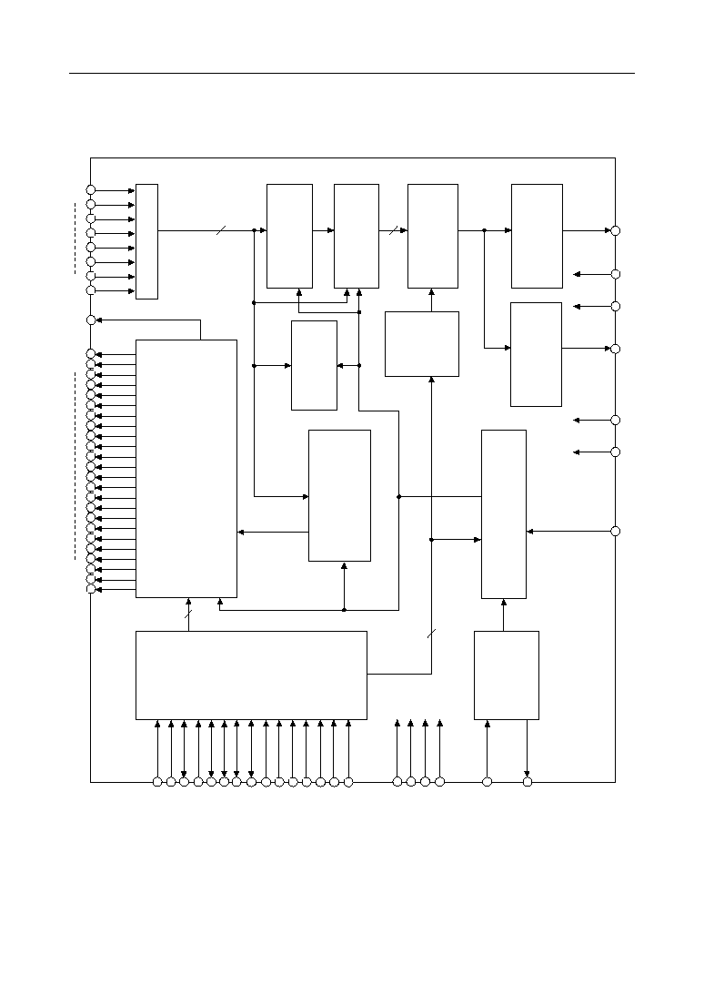
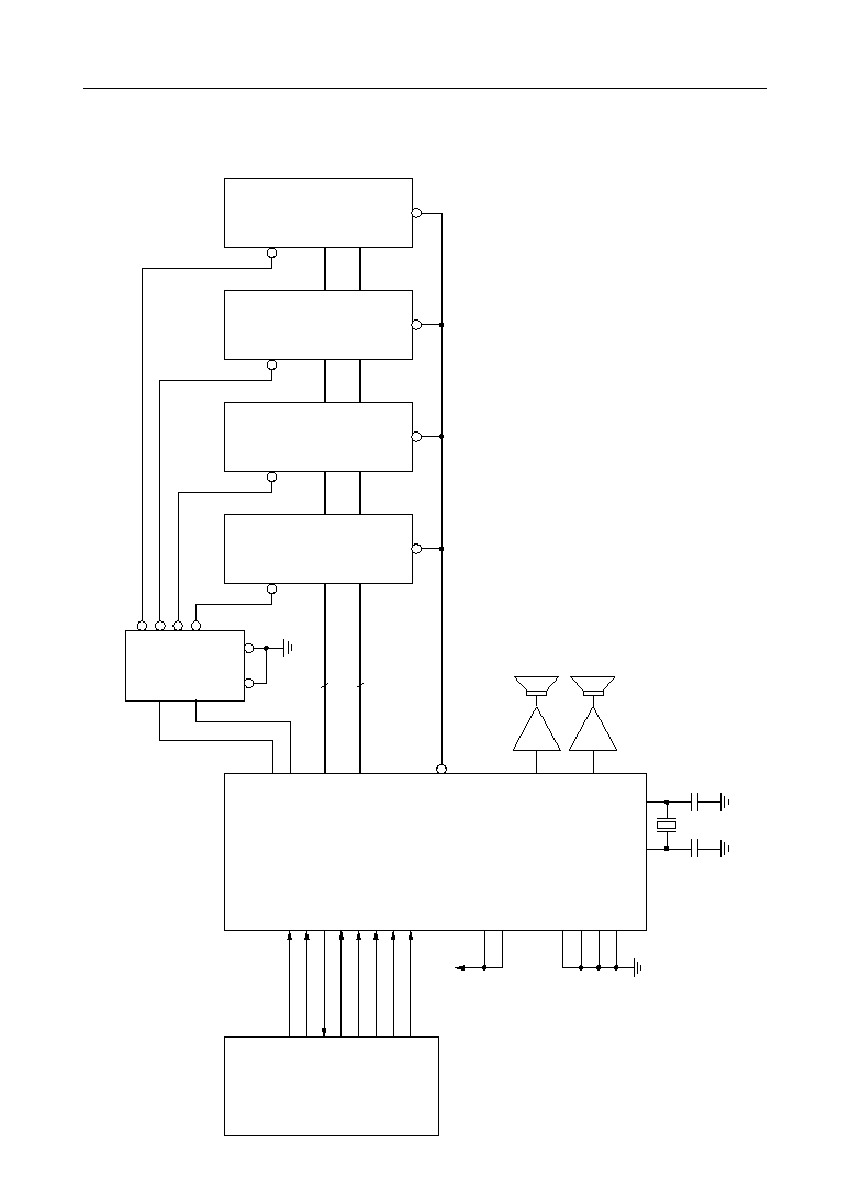
BLOCK DIAGRAM
8-Bit LATCH
23-Bit Multiplexer
CPU
interface
8
ADPCM
Synthesizer
PCM
Synthesizer
16
8
14-Bit
DAC
RDAO
DATA
Controller
23-Bit Address
Counter
Timing Controller
DGND
DV
DD
OSC
D7/SD
D6/SI
D5/SO
D4/UD
D3/SR3
D2/SR2
D1/SR1
D0/SR0
RCS
CS
WR
RD
CMD
SERIAL
NCR/BUSY
XT
XT
RESET
RA23
RA0
RD7
RD0
14-Bit
DAC
LDAO
16*9 MPY
8
PAN
Register
ROE
AGND
AV
DD
TEST1
TEST2
TEST3
TEST4

3/31
° Semiconductor
MSM9810
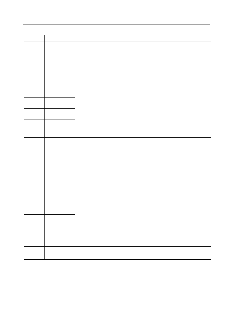
PIN CONFIGURATION (TOP VIEW)
NC: No connection
64-pin Plastic QFP
48
47
46
45
44
43
42
41
40
39
38
1
2
3
4
5
6
7
8
9
10
11
DGND
AGND
TEST4
LDAO
RDAO
AV
DD
DV
DD
RCS
TEST1
TEST2
XT
DV
DD
RA8
RA7
RA6
RA5
RA4
RA3
RA2
RA1
ROE
RD0
64
63
62
61
60
59
58
57
56
55
54
RA23
RA22
RA21
RA20
RA0
RA17
RA16
RA15
RA14
RA13
RA12
17
18
19
20
21
22
23
24
25
26
27
NC
WR
NCR/
BUSY
CS
D0/SR0
D1/SR1
D2/SR2
D3/SR3
D4/UD
D5/SO
D6/SI
12
XT
13
TEST3
14
SERIAL
15
CMD
16
RD
28
D7/SD
29
RESET
30
RD7
31
RD6
32
DGND
37 RD1
36 RD2
35 RD3
34 RD4
33 RD5
53
RA11
52
RA10
51
RA9
50
RA19
49
RA18

4/31
° Semiconductor
MSM9810
PIN DESCRIPTIONS
Symbol
Type
RA23-RA0
O
Address pins for external memory. These pins become high impedance
when RCS pin is "H".
RD7-RD0
I
Data pin for external memory. Pull-down resistors are internally
connected to these pins. These pull-down resistors become valid when
the RCS pin is "H", and become invalid when the RCS pin is "L".
ROE
O
Output enable pin for external memory.
CMD
I
Select pin for Command data or Subcommand data.
When this pin is "H", subcommand input is selected. When this pin is "L",
command input is selected.
A pull-up resistor is internally connected to this pin.
RD
I
Read pin for CPU interface.
A pull-up resistor is internally connected to this pin.
WR
I
Write pin for CPU interface.
A pull-up resistor is internally connected to this pin.
CS
I
Chip select pin for CPU interface. When CS is "H", WR signal is not
entered in this IC. A pull-up resistor is internally connected to this pin.
D7/SD
I/O
Data bus pin for CPU interface when parallel input interface is selected.
When WR is "L", this pin serves as data input pin.
When RD is "L", this pin serves as channel status data output pin.
When serial input interface is selected, this pin serves as serial data
input pin.
D6/SI
I/O
Data bus pin for CPU interface when parallel input interface is selected.
When WR is "L", this pin serves as data input pin.
When RD is "L", this pin serves as channel status output pin.
When serial input interface is selected, this pin serves as serial clock
input pin.
D5/SO
I/O
Data bus pin for CPU interface when parallel input interface is selected.
When WR is "L", this pin serves as data input pin.
When RD is "L", this pin serves as channel status output pin.
When serial input interface is selected, this pin serves as channel status
output pin.
Description
Pin
40-47, 49-64
30, 31, 33-38
39
15
16
18
20
28
27
26
RCS
I
When this pin is "L", RA23 to RA0 and ROE pins output address data and
output enable signal.
When this pin is "H", RA23 to RA0 and ROE pins become high impedance.
8
SERIAL
I
CPU interface select pin. When SERIAL is "H", serial input interface is
selected.
When it is "L", parallel input interface is selected.
14
5/31
° Semiconductor
MSM9810
LDA0
O
LEFT side D/A output pin.
RDA0
O
RIGHT side D/A output pin.
XT
I
Crystal or ceramic oscillator connection pin.
A feedback resistor of about 1MW is connected between XT and XT.
If necessary, enter external clocks into this pin.
XT
O
Crystal or ceramic oscillator connection pin.
When external clocks are used, leave this pin open.
Data bus pin for CPU interface when parallel input interface is selected.
When WR is "L", this pin serves as data input pin.
When RD is "L", this pin serves as channel status output pin.
When serial input interface is selected, this pin serves as channel status
output pin.
When UD is "H", channels 8 thru 5 are output to SR3 thru SR0, respectively.
When UD is "L", channels 4 thru 1 are output to SR3 thru SR0, respectively.
D0/SR0
I/O
D1/SR1
D2/SR2
D3/SR3
When this pin is "L" level, the LSI is initialized. At that time, oscillation
stopsand D/A outputs go to GND level.
RESET
I
NCR/BUSY
I
Channel status select pin.
When this pin is "H", NCR signal is output. When it is "L", BUSY signal is
output.
TEST1
I
Pins for IC testing. Apply "L" level to these pins.
Pull-down resistors are internally connected to these pins.
DV
DD
--
Power supply pin.
DGND
--
GND pin.
24
23
22
21
4
5
11
12
29
19
9
7, 48
1, 32
TEST2
AV
DD
AGND
10
6
2
TEST3
13
Symbol
Type
Description
Pin
TEST4
3
I
Pins for IC testing. Apply "L" level to these pins.
D4/UD
I/O
Data bus pin for CPU interface when parallel input interface is selected.
When WR is "L", this pin serves as data input pin.
When RD is "L", this pin serves as channel status output pin.
When serial input interface is selected, this pin serves as channel status
selecter pin.
When UD is "H", channels 8 thru 5 are output to SR3 thru SR0, respectively.
When UD is "L", channels 4 thru 1 are output to SR3 thru SR0, respectively.
25
6/31
° Semiconductor
MSM9810
ABSOLUTE MAXIMUM RATINGS
Parameter
Symbol
Condition
Rating
Unit
V
DD
V
IN
T
STG
Power Supply Voltage
Input Voltage
Storage Temperature
Ta=25∞C
≠0.3 to +7.0
≠0.3 to V
DD
+0.3
≠55 to +150
V
V
∞C
--
(GND=0 V)
RECOMMENDED OPERATING CONDITIONS
ELECTRICAL CHARACTERISTICS
DC Characteristics
Parameter
Symbol
Condition
Range
Unit
(GND=0 V)
Power Supply Voltage
V
DD
--
3.5 to 5.5
V
Operating Temperature
T
op
--
≠40 to +85
∞C
Master Clock Frequency
f
OSC
--
Typ.
MHz
4.096
Min.
Max.
3.5
4.5
Parameter
Symbol
Condition
Min.
Unit
(DV
DD
=AV
DD
=4.5 to 5.5 V, DGND=AGND=0 V, Ta=≠40 to +85∞C)
Typ.
Max.
High-level Input Voltage
V
IH
--
0.84•V
DD
V
--
--
Low-level Input Voltage
V
IL
--
--
V
--
0.16•V
DD
High-level Output Voltage
V
OH
I
OH
= ≠1mA
V
DD
≠0.4
V
--
--
Low-level Output Voltage
V
OL
I
OL
= 2mA
--
V
--
0.4
High-level Input Current 1
I
IH1
V
IH
= V
DD
--
mA
--
10
Low-level Input Current 1
I
IL1
V
IL
= GND
≠10
mA
--
--
Operating Current
I
DD
--
--
mA
6
15
Standby Current
I
DS
Ta
= ≠40∞C to +70∞C
--
mA
--
15
Output Leakage Current
I
LO
0 £ V
OUT
£ V
DD
≠10
mA
--
+10
Ta
= ≠40∞C to +85∞C
--
mA
--
50
High-level Input Current 2
I
IH2
Applied to pins with internal
pull-down resistor
30
mA
--
300
Low-level Input Current 2
I
IL2
Applied to pins with internal
pull-up resistor
≠300
mA
--
≠30
7/31
° Semiconductor
MSM9810
AC Characteristics
Parameter
Symbol Min.
Unit
f
duty
t
w(RST)
t
D(RST)
t
CR
t
RR
t
DRE
t
DRF
t
DW
t
CW
t
WW
t
DWS
t
DWH
t
WWS
t
CC
t
SDS
t
SSD
t
W(SCK)
Master Clock Duty Cycle
RESET Input Pulse Width
RESET Delay Time From Raising of Power Supply
Set up and Hold Time of CS for RD, at serial input I/F
RD Pulse Width
Output Data Valid Time after Fall of RD
Data Float Time after Rise of RD
Setup and Hold Time of CMD for WR
Setup and Hold Time of CS for WR
WR Pulse Width
Data Setup Time before Rise of WR
Data Hold Time after Rise of WR
WR-WR Pulse Interval
CS-CS Pulse Interval
Serial Data Setup Time
Serial Data Hold Time
Serial Clock Pulse Width
40
1
0
30
200
--
--
50
30
200
100
30
160
100
30
30
200
%
ms
ms
ns
ns
ns
ns
ns
ns
ns
ns
ns
ns
ns
ns
ns
ns
(V
DD
=3.5 to 5.5V, GND=0 V, Ta=≠40 to +85∞C)
Typ.
Max.
50
--
--
--
--
--
10
--
--
--
--
--
--
--
--
--
--
60
--
--
--
--
100
50
--
--
--
--
--
--
--
--
--
--
8/31
° Semiconductor
MSM9810
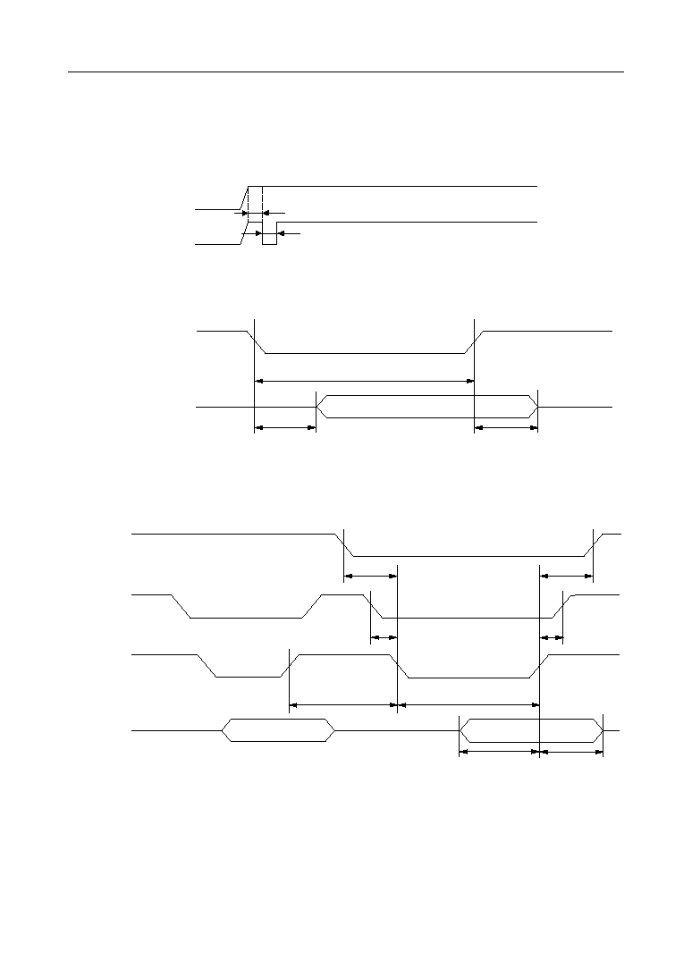
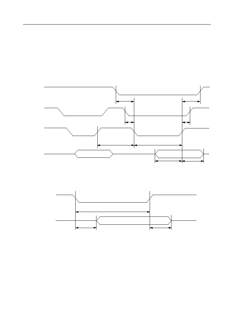
TIMING DIAGRAMS
Power-On Timing
V
DD
RESET (I)
t
W(RST)
t
D(RST)
Data Read Timing, Parallel Input
t
DRE
t
RR
Data out Valid
RD(I)
D7 - D0(I/O)
t
DRF
Data Write Timing, Parallel Input
t
DWS
t
WW
t
CW
Data Stable
CS(I)
WR(I)
D7 - D0(I)
t
DWH
t
CW
Data Stable
t
DW
CMD(I)
t
WSS
t
DW
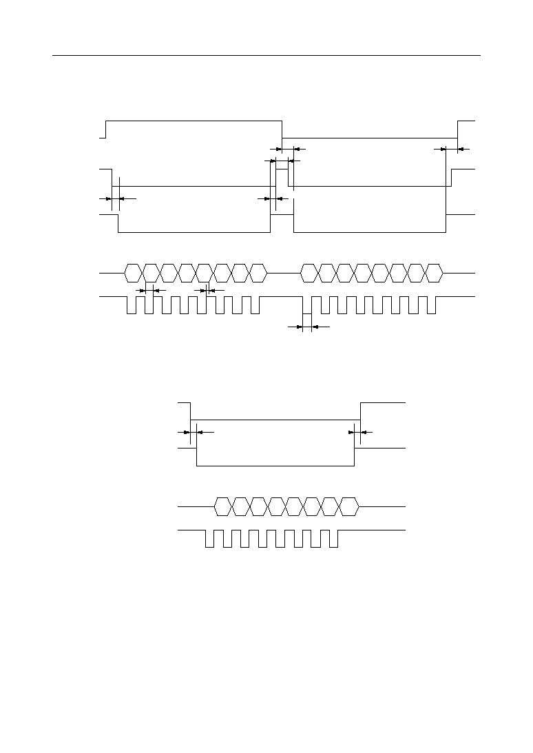
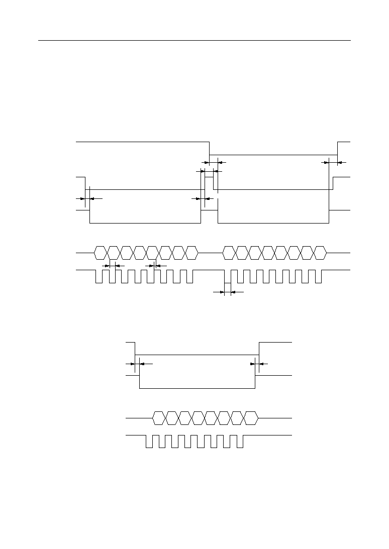
9/31
° Semiconductor
MSM9810
Data Write Timing, Serial Input
Data Read Timing, Serial Input
CS(I)
WR(I)
SD(I)
CMD(I)
SI(I)
t
W(SCK)
t
CW
t
DW
t
CC
t
SDS
t
SSD
t
DW
t
CW
CS(I)
RD(I)
SO(I)
SI(I)
t
CR
t
CR
10/31
° Semiconductor
MSM9810
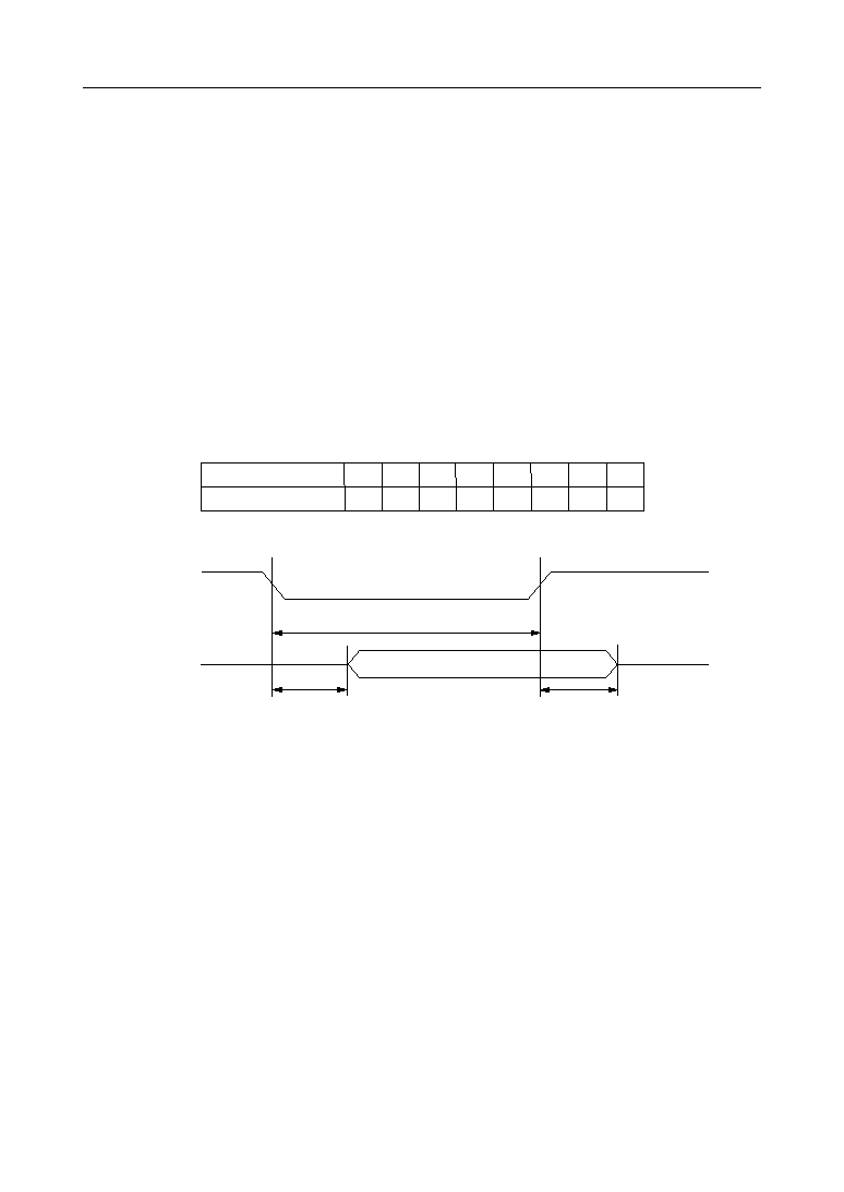
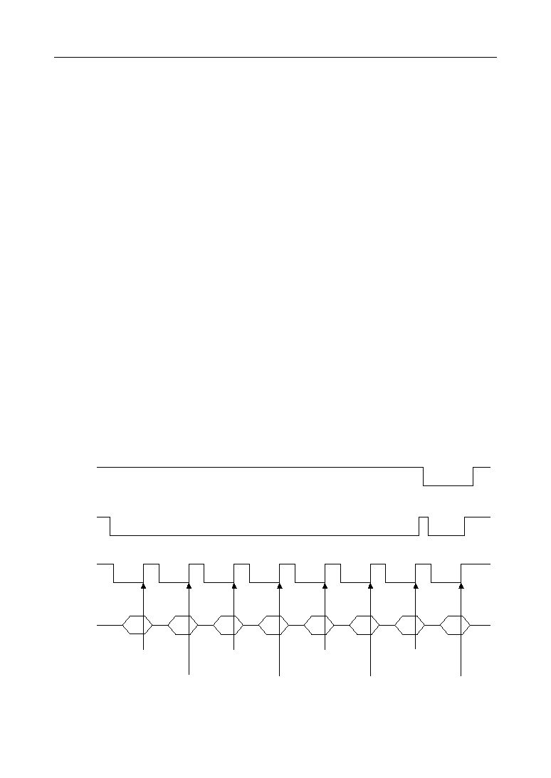
Command input timing in parallel input interface
∑ The phrase address "25H" data is played back via channel 1
∑ The command options selected are 1/2 V
DD
(P-P) sound volume for all channels, use of an
internal low pass filter, secondary digital filter processing, and voltage follower output.
CS
CMD
WR
D7-D0
09H
18H
25H
28H
01H
00H
Set option data
Subcommand
(OPT)
Transfer option
data Command
(OPT)
Set address
data Subcommand
(FADR)
Transfer address
data to channel 1
Command
(FADR)
Set Start flag
to channel 1
Subcommand
(START)
Start flag execution
(Channel 1)
Command
(START)
Channel 1 voice
systhesis starts
See 9. "Command Data and Subcommand Data" for further information on commands and subcommands.
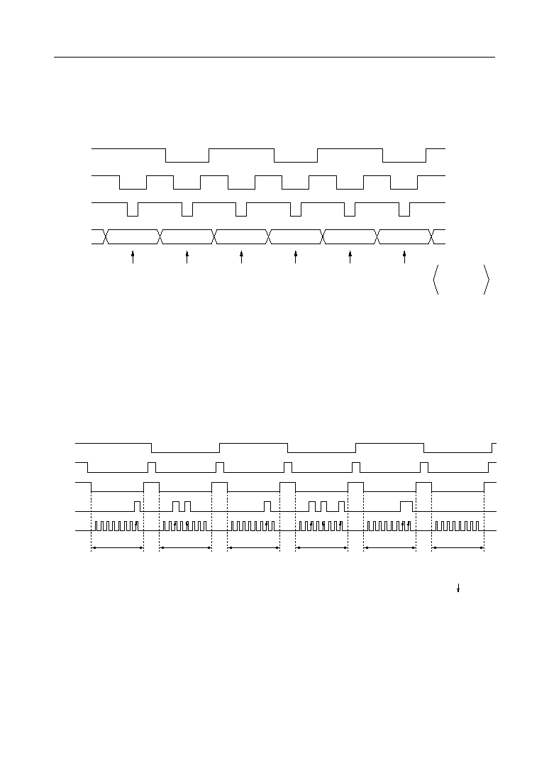
Command input timing in serial input interface
∑ Phrase address "08H" to channel 1 data and Phrase address "02H" to channel 2 data are played
back simultaneously.
∑ The command option is default setting.
CS
CMD
WR
SD
Set address "01H" data
Subcommand
(FADR)
SI
(08H)
Transfer address
data to channel 1
Command
(FADR)
(28H)
Set address "02H" data
Subcommand
(FADR)
(02H)
Transfer address data
to channel 2
(FADR)
(29H)
Set start flag to channel 1
and channel 2
Subcommand
(START)
(03H)
Start flag execution
(channel 1 and channel 2)
Command (START)
(00H)
Channel 1 and channel 2
voice synthesis starts
See 3-1 "Channel Synthesis" for further information on channel synthesis.

11/31
° Semiconductor
MSM9810
FUNCTIONAL DESCRIPTION
1. User Specification Phrase
A maximum of 256 phrases can be selected with user specification phrases. User specification
phrases are stored in the voice management area of external ROM. Merely by selecting a phrase,
sampling frequency and the start and stop address of voice are controlled.
The MSM9810 can directly specify a start address or stop address externally without using user
specification phrases. Only channels 1 to 4 can be used for directly specifying a start address or
stop address externally.
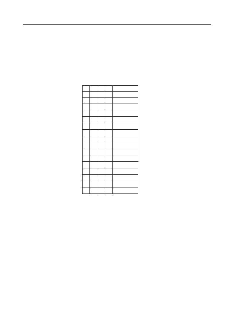
2. Playback Time and Memory Capacity
Table 2.1 shows the configuration of external ROM. The capacity of an actual voice data ROM is
different from the indicated ROM capacity.
Table 2.1 ROM Configuration
Address management area (16Kbits)
Voice data area or
Phrase Controll Table area
Playback time depends on external memory capacity, sampling frequency, and the playback
system. The relationship is shown below.
For example, when one 8 Mbits ROM is used with a 16 kHz sampling frequency in a 4-bit ADPCM
type, the playback time becomes as follows.
1.024 • (8192≠16) Kbits
Playback time=
16 (kHz) • 4 (bit)
=131 seconds
.
.
In the above equation, the playback time when the Phrase Controll Table function is not used is
shown.
1.024 • (memory capacity ≠16) (Kbits)
Playback time =
Sampling frequency (kHz) • bit length
(Seconds)
(Bit length is ADPCM, ADPCM2...4bits, PCM...8bits)
12/31
° Semiconductor
MSM9810
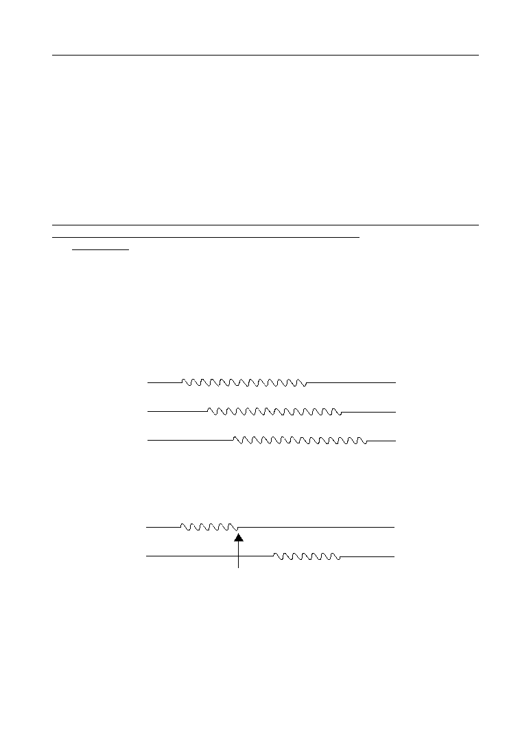
Channel 1
Channel 2
Channel 3
f
S
=16.0kHz
f
S
=32.0kHz (Valid)
f
S
=25.6 kHz (Invalid, playback with f
S
=32.0 kHz)
Figure 3.1 When channel 3 is played back using a different sampling frequency
while channel 1 and 2 are being played back.
Channel 1
Channel 2
f
S
=16.0kHz
f
S
=25.6kHz (Valid)
Channel 1 ends
Figure 3.2 Channel 2 is played back using different sampling frequency
after channel 1 was played back
3. Sampling Frequency
Sampling frequency can be specified for each phrase in the address management area of external
ROM. For the sampling frequency, the following ten types can be selected when voice data is
created.
4.0 kHz, 8.0 kHz, 16.0 kHz, 32.0 kHz
(Group 1)
5.3 kHz, 10.6 kHz, 21.3 kHz
(Group 2)
6.4 kHz, 12.8 kHz, 25.6 kHz
(Group 3)
3-1 Channel Synthesis
When the internal LPFs are used, use of a different sampling frequency than the selected
sampling frequency GroupX is not permitted for channel synthesis.
The internal LPF can be used by selecting "use of internal LPF" with the OPT command (see 9-
4 "OPT Command").
When the internal LPFs are not used, channel synthesis can be made using a different sampling
frequency as shown below.
When channels are synthesized, the sampling frequency Group of the first vocalizing channel
(one of the above Group 1 to 3) is selected. If the sampling frequency Group other than the
selected Group is used for channel synthesis, playback becomes fast or slow. Figure 3.1 and
Figure 3.2 show examples.

13/31
° Semiconductor
MSM9810
When multiple channels are played back simultaneously, the sampling frequency Group of the
smallest channel has priority.
Channel 3
Channel 4
Channel 8
f
S
=8.0 kHz (Sampling frequency group of channel 3 is selected.)
f
S
=25.6 kHz (Invalid, playback with fs=32.0 kHz)
f
S
=32.0 kHz (Valid)
Figure 3.3 When channel 3, 4 and 8 are played back simultaneously.

14/31
° Semiconductor
MSM9810
4. Reset Function
When "L" level is input to the RESET pin, LSI enters power down state, stopping oscillation and
minimizing current consumption. At the same time, the control circuit is reset and initialized.
Power down status is as follows.
(1)
Oscillation stops and all internal circuits stop operation.
(2)
Current consumption is minimized. When an external clock is in use, input "L" level
to the XT pin in power down status, so that current does not flow into the oscillation
circuit.
(3)
When a crystal oscillator is in use, "L" level is output to the XT pin.
(4)
GND level is output to the D/A output pin (LDAO, RDAO).
Be certain to input "L" level to the RESET pin when power is turned on.
5. Playback System
This LSI has four types of playback systems to support various voices: 4-bit ADPCM, 4-bit
ADPCM2, 8-bit straight PCM, and 8-bit non-linear PCM.
5-1 4-bit ADPCM
ADPCM (Adaptive Differential Pulse Code Modulation) system adaptively changes the
quantization width and encodes 4-bit data for each sampling, so that the follow up to a voice
waveform improves.
ADPCM data is converted by using an analysis tool.
For a human voice, animal voice and natural sounds, it is better to use the ADPCM system
because the voice data capacity decreases.
5-2 4-bit ADPCM2
In 4-bit ADPCM 2, the follow-up characteristics to a voice waveform is even better than the 4-bit
ADPCM. This system is compatible only with MSM9841/MSM9842.
ADPCM2 data is converted by using an analysis tool.
5-3 8-bit Straight PCM
The follow-up characteristics to a voice waveform to all voice areas is the best of all four types.
This system is suitable for sound effects, where waveforms change rapidly, and for pulse shape
waveforms.
5-4 8-bit Non-linear PCM
This system plays back the center of a waveform to be a voice quality equivalent to 10 bits. This
system is to improve the voice quality of low volume sounds.
8-bit non-linear PCM data is converted by using an analysis tool.

15/31
° Semiconductor
MSM9810
6. Voice Output
The voice is output as 14-bit D/A converter output in stereo (LDAO, RDAO), with L/R in phase.
The output amplitude from the D/A converter has a maximum (16383/16384) • V
DD
, and the
output waveform has a step waveform synchronized with sampling frequency.
The command option has been set for voice output. D/A converter output and voltage follower
output can be selected by option.
7. Microcomputer Interface
There are two types of interface with microcomputer; one is parallel input interface and the other
is serial input interface. Either of the two interfaces can be selected with the SERIAL pin. The
parallel input interface is selected when SERIAL is at a "L" level.
The serial input interface is selected when SERIAL is at "H" level.
When the parallel input interface is selected, the MSM9810 is controlled by nine different
commands using D7 to D0 (data buses) and control pins CMD, CS, WR, and RD. The internal
status register is used to check the status of the LSI.
When the serial input interface is selected, the MSM9810 is controlled by nine different
commands using serial data input pin SD and serial clock input pin SI, and control pins CMD,
CS, WR, and RD.
The SO, SR3, SR2, SR1 and SR0 pins are used to check the status of the LSI.
The pins 21 to 28 function differently according to whether the parallel input interface is selected
or the serial input interface is selected.
The table 7-1 shows the pin names. See "PIN DESCRIPTIONS" for their functions.
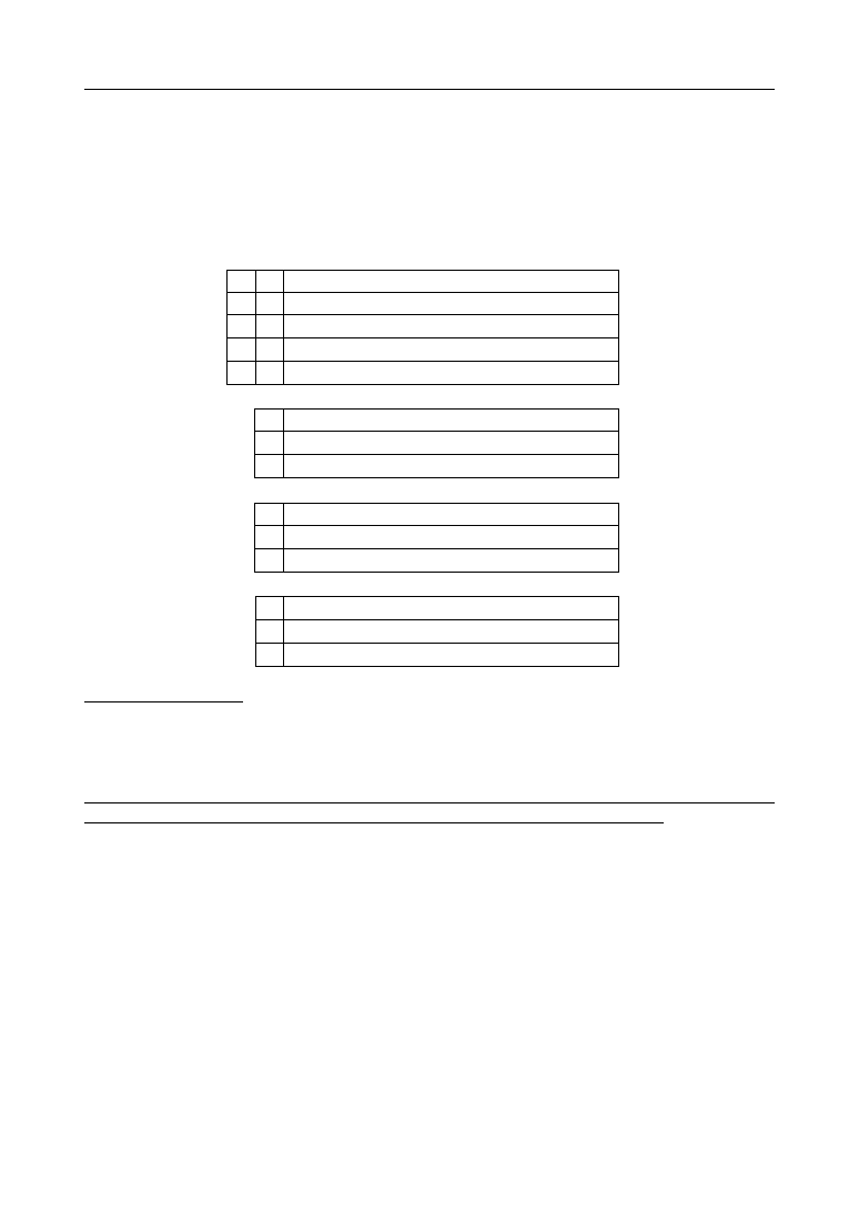
Table 7-1 Difference between parallel input and serial input pins
28
D0
SR0
27
D1
SR1
26
D2
SR2
25
D3
SR3
24
D4
UD
23
D5
SO
22
D6
SI
21
D7
SD
Pin number
Parallel input
Serial input
16/31
° Semiconductor
MSM9810
7-1 Parallel Input Interface
In the parallel input interface, the microcomputer controls the LSI via 13 pins of RESET, CMD,
CS, WR, RD and D7-D0.
Command and subcommand data are input from D7-D0 by control of CMD, CS and WR, as
shown in Figure 7-1, and the status is output from D7-D0 by control of RD, as shown in Figure
7-2.
Figure 7-1 Parallel input write cycle timing
t
DRE
t
RR
Data out Valid
RD(I)
D7 - D0(I/O)
t
DRF
Figure 7-2 Parallel input read cycle timing
t
DWS
t
WW
t
CW
Data Stable
CS(I)
WR(I)
D7 - D0(I)
t
DWH
t
CW
Data Stable
t
DW
CMD(I)
t
WSS
t
DW
17/31
° Semiconductor
MSM9810
7-2 Serial Input Interface
In the serial input interface, the microcomputer controls the LSI via 8 pins of RESET, CMD, CS,
WR, RD, SD, SI and SO. In parallel input, data is output from D7-D0, but in serial input, data for
D7-D0 is input in serial from MSB using SD and SI.
Figure 7-3 shows the command and subcommand input timing, and Figure 7-4 shows read
timing.
Figure 7-3 Serial input write cycle timing
CS(I)
RD(I)
SO(I)
SI(I)
t
CR
t
CR
Figure 7-4 Serial input read cycle timing
CS(I)
WR(I)
SD(I)
CMD(I)
SI(I)
t
W(SCK)
t
CW
t
DW
t
CC
t
SDS
t
SSD
t
DW
t
CW
18/31
° Semiconductor
MSM9810
8. Channel Status
The channel status is output from D7-D0.
There are two types of signals to be output as channel status: BUSYn (n = 1-8) signals and NCRn
signals. These two types are selected by the NCR/BUSY pin. When the NCR/BUSY pin is at "H"
level, NCR is output, and when at "L" level, BUSY is output.
The NCR signal is the command and subcommand input status signal (Next Command Request)
of each channel, and the WR signal input is enabled at "H" level.
The BUSY signal outputs "L" level while each channel is executing voice synthesis.
Each channel status signal is output from D7-D0 pins in parallel input interface, and from D5/
S0 pins and D3/SR3-D0/SR0 pins in serial input interface by control of RD. Table 8-1 shows the
relationship between D7-D0 and channels, and Figure 8-1 shows read timing in the parallel input
interface.
Table 8-1 Correspondence between D7-D0 and channels
Data bus
Corresponding channel
D7
D6
D5
D4
D3
D2
D1
D0
CH8 CH7 CH6 CH5 CH4 CH3 CH2 CH1
t
DRE
t
RR
Data out Valid
RD(I)
D7 - D0(I/O)
t
DRF
Figure 8-1 Read timing in parallel input interface
In serial input interface, serial output from D5/SO pins by control of CS and RD, and D3/SR3-
D0/SR0 parallel output (constantly output) can be selected.
For serial output from D5/SO pin, D7-D0, shown in Table 8-1, are output from MSB in serial at
the rise of the SI pin when the RD pin is at "L" level.
Figure 8-2 shows this timing.
19/31
° Semiconductor
MSM9810
SI(I)
D7
SO(O)
RD(I)
D6 D5 D4 D3 D2 D1 D0
CS
UD
SR3
CH8
CH4
SR2
CH7
CH3
SR1
CH6
CH2
SR0
CH5
CH1
CH8-5
CH4-1
Figure 8-2 Read timing in serial input interface
In serial input interface, status signals are constantly output from D3/SR3 to D0/SR0 pins.
Selection of NCR and BUSY is controlled by the NCR/BUSY pin. Since there are only four D3/
SR3 to D0/SR0 pins, 8 channels of status signals are selected by control of the D4/UD pin. Table
8-2 shows the relationship between D4/UD pin and D3/SR3 to D0/SR0 pins.
Table 8-2 Correspondence between D4/UD and D3/SR3 to D0/SR0
Channel 4
Channel 3
Channel 2
Channel 1
D3/SR3
D2/SR2
D1/SR1
D0/SR0
D4/UD="L"
Channel 8
Channel 7
Channel 6
Channel 5
D4/UD="H"
20/31
° Semiconductor
MSM9810
9. Command Data and Subcommand Data
In parallel input, command data and subcommand data are controlled by the data bus of D7-D0
pins and by CMD, CS and WR control pins. In serial input, command data and subcommand data
are controlled by data input/output of SD, SI and SO pins and by CMD, CS and WR control pins.
This LSI reads data to the internal register (TMP register) by executing the subcommand, and
transfers data of the TMP register to the register of each command function and executes data by
executing the command.
A subcommand and command are distinguished by the level of the CMD pin. "H" level indicates
a subcommand, and "L" level indicates a command.
Table 9-1 shows the command data list, Table 9-2 shows details of C2-C0 of Table 9-1 (channel
specification), and Table 9-3 shows subcommand data list corresponding to command data.
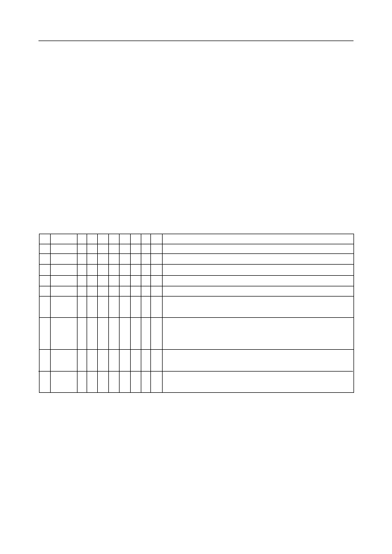
Table 9-1 Command Data List
(X - - - don't care. For C1, C2 and C0, see Table 9-2.)
D7 D6 D5 D4 D3 D2 D1 D0
Function
Starts playback of the channel for which data stored in the register is "H".
Stops playback of channel for which data stored in the register is "H".
Repeats playback of channel for which data stored in the regiter is "H".
Changes option by command.
Inserts silence corresponding to the length of data stored in the register.
Transfers phrase address stored in the register to the phrase register
of the specified channel.
This command internally transfers the 7-byte start and stop address,
the value of sampling frequency and playback algorithm which are
stored in the TMP register.
Changes volume of the specified channel to the volume of data stored
in the register.
Changes volume of the right and left D/A converter to volume of data
stored in the register.
0
0
0
0
0
0
0
0
0
0
0
0
0
0
0
0
0
1
0
0
0
0
1
1
1
1
0
0
0
1
1
0
0
1
1
0
0
1
0
1
0
1
0
1
0
START
STOP
LOOP
OPT
MUON
FADR
DADR
CVOL
PAN
1
2
3
4
5
6
7
8
9
X
X
X
X
C2
C2
C2
C2
C2
X
X
X
X
C1
C1
C1
C1
C1
X
X
X
X
C0
C0
C0
C0
C0
21/31
° Semiconductor
MSM9810
C2
Channel control
Channel 1
Channel 2
Channel 3
Channel 4
Channel 5
Channel 6
Channel 7
Channel 8
0
0
1
1
0
0
1
1
0
1
0
1
0
1
0
1
0
0
0
0
1
1
1
1
C1 C0
Table 9-2 Channel Specification List
Subcommand funciton
Channel setting
Channel setting
Channel setting
Option setting
Silence time setting
Phrase address setting
(1st byte) address setting
(2nd byte)
(3nd byte)
(4nd byte)
(5nd byte)
(6nd byte)
(7nd byte)
Volume setting
Volume setting
START
STOP
LOOP
OPT
MUON
FADR
DADR
CVOL
PAN
CH8
CH8
CH8
0
M7
FA7
SA23
SA15
SA7
ST23
ST15
ST7
S3
X
L3
CH7
CH7
CH7
0
M6
FA6
SA22
SA14
SA6
ST22
ST14
ST6
S2
X
L2
CH6
CH6
CH6
0
M5
FA5
SA21
SA13
SA5
ST21
ST13
ST5
S1
X
L1
CH5
CH5
CH5
O4
M4
FA4
SA20
SA12
SA4
ST20
ST12
ST4
S0
X
L0
CH4
CH4
CH4
O3
M3
FA3
SA19
SA11
SA3
ST19
ST11
ST3
P1
V3
R3
CH3
CH3
CH3
O2
M2
FA2
SA18
SA10
SA2
ST18
ST10
ST2
P0
V2
R2
CH2
CH2
CH2
O1
M1
FA1
SA17
SA9
SA1
ST17
ST9
ST1
X
V1
R1
CH1
CH1
CH1
O0
M0
FA0
SA16
SA8
SA0
ST16
ST8
ST0
X
V0
R0
Command
D7
D6
D5
D4
D3
D2
D1
D0
(X - - - don't care.)
Table 9-3 Subcommand Data List
22/31
° Semiconductor
MSM9810
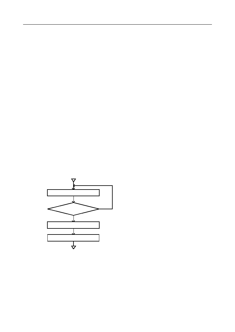
9-1 START Command
The START command starts voice synthesis of the channel corresponding to the data stored in
the TMP register. Table 9-4 shows the correspondence between data input (D7-D0) and channels.
For serial input, the sequence of D7-D0 and serial input data is shown in Figure 8-2.
Table 9-4 Correspondence between D7-D0 and Channels
Data bus
Corresponding channel
D7
D6
D5
D4
D3
D2
D1
D0
CH8 CH7 CH6 CH5 CH4 CH3 CH2 CH1
When the START command is input, data stored in the TMP register is set at the start register,
and voice synthesis processing starts. For example, when all " 1" is written from the data bus to
the TMP register and the START command is input, all channels start voice synthesis
simultaneously.
Input the START command when the status signal (NCR or BUSY) of the channel to be started
is at "H". When NCR is "L", input is disabled.
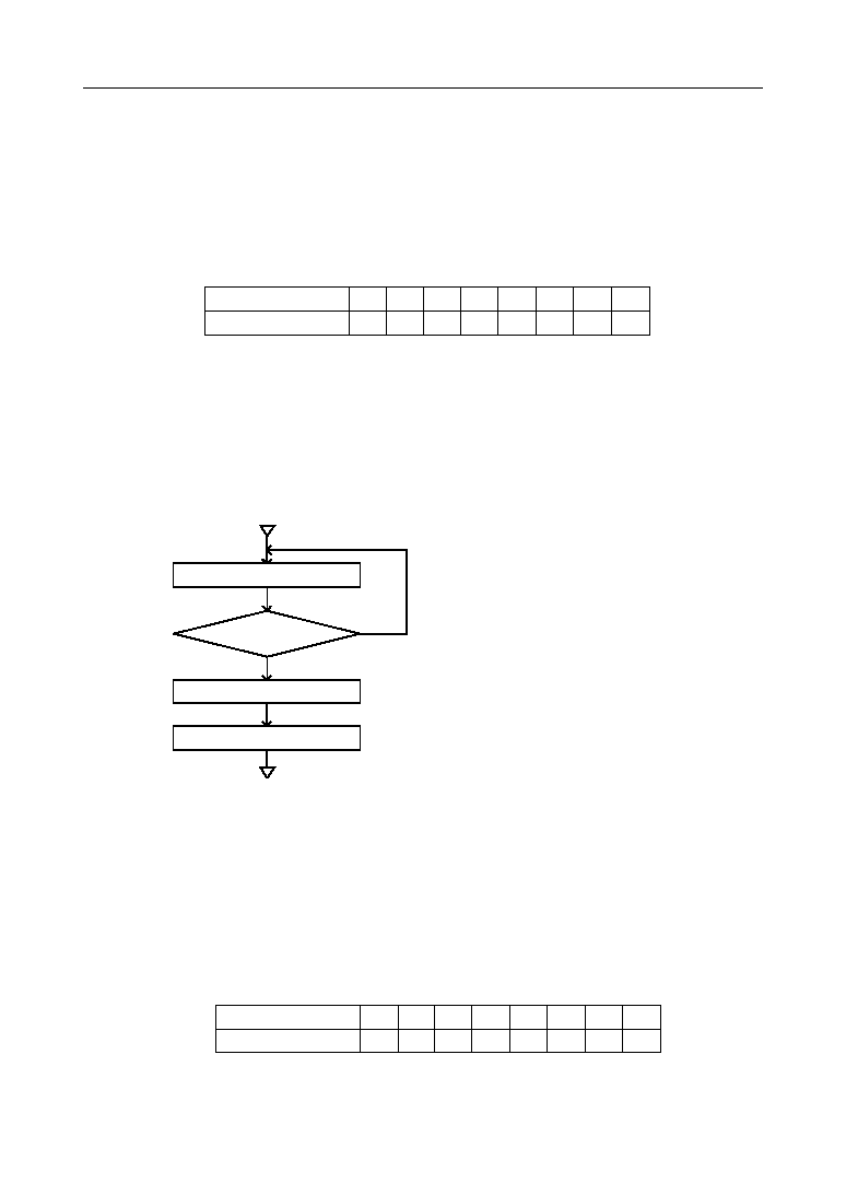
Figure 9-1 shows the flowchart when the START command is input.
Subcommand input
RD pulse input
NCRn="H"
START command input
NO
YES
NCRn corresponding to each channel is output
to D7-D0
Check that D7-D0 corresponding to the channel
to start voice synthesis is "H".
After setting "H" to D7-D0 corresponding to the
channel to start voice synthesis from the data
bus, input the WR pulse. (Set CMD to "H".)
Figure 9-1 START Command Input Flow
9-2
STOP Command
The STOP command stops voice synthesis processing of the channel corresponding to data
stored in the TMP register. Table 9-5 shows the correspondence between data input (D7-D0) and
channels.
Table 9-5 Correspondence between D7-D0 and channels
Data bus
Corresponding channel
D7
D6
D5
D4
D3
D2
D1
D0
CH8 CH7 CH6 CH5 CH4 CH3 CH2 CH1
23/31
° Semiconductor
MSM9810
When the STOP command is input, the LSI stops processing of voice synthesis of the corresponding
channel at the rise of the WR pulse. When voice synthesis stops, the PCM value of that channel
is cleared to 1/2 V
DD
, and the NCR and BUSY channel status signals become "H".
When "H" has been set at the START register, the START register is cleared to "L".
9-3
LOOP Command
The LOOP command repeats a playback of voice synthesis of the channel corresponding to data
stored in the TMP registers. Table 9-6 shows the correspondence between data input (D7-D0) and
channels.
Table 9-6 Correspondence between D7-D0 and channels
Data bus
Corresponding channel
D7
D6
D5
D4
D3
D2
D1
D0
CH8 CH7 CH6 CH5 CH4 CH3 CH2 CH1
When the LOOP command is input, the LSI writes data of the TMP register to the LOOP register
at rise of WR pulse, and repeats a playback of the channel where "H" is set. Once "H" is set at
the LOOP register, playback continues until "L" is set from the outside. If the phrase controll table
function has been used for a phrase address, the edited voice is repeatedly played back.
To end a repeating playback, set the register of the channel to end the repeat to "L" using the
LOOP command again. When the register is set to "L", repeating ends with the current playback
phrase. If the START register has been set to continue the playback of another phrase, another
phrase is played back continuously after repeating ends.
Figure 9-2 shows an example.
Channel 1
LOOP start
1 phrase
1 phrase
1 phrase
2 phrase
LOOP end
Figure 9-2 LOOP Command Execution Example
24/31
° Semiconductor
MSM9810
9-4 OPT Command
The OPT command changes the setting inside the LSI according to data stored in the TMP
register. Table 9-7 shows the correspondence between data input (D7 to D0) and options.
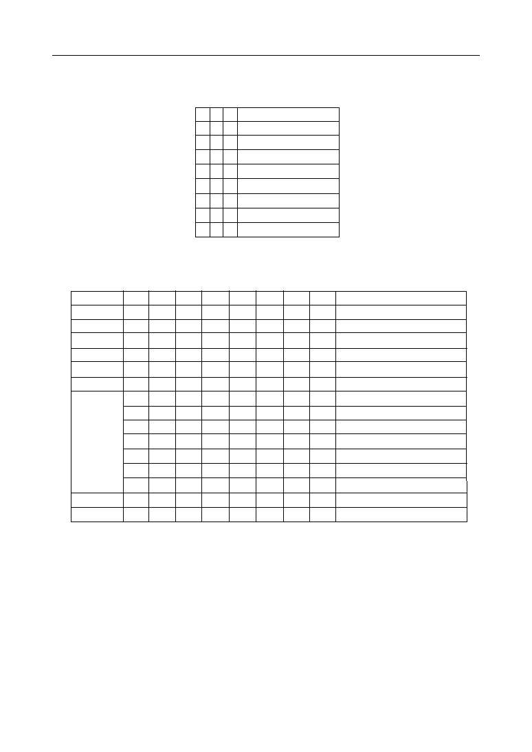
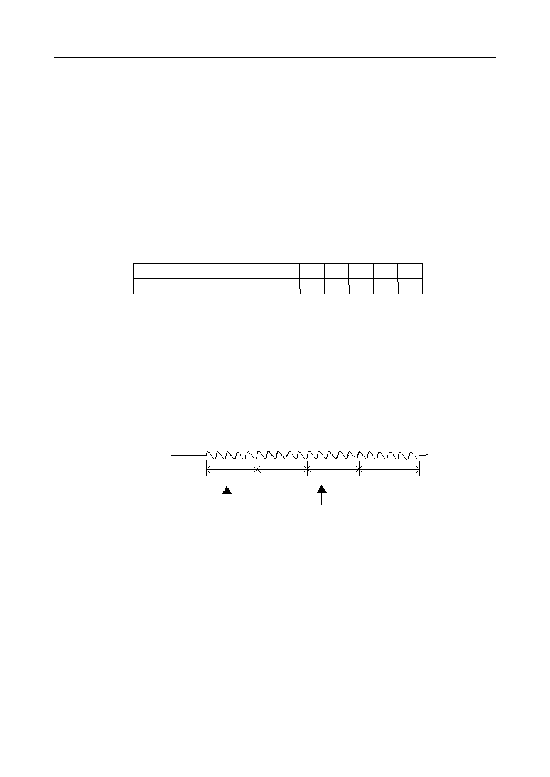
Table 9-7 Correspondence between D7-D0 and options
(Input "L" to D7-D5.)
When the OPT command is input, the LSI changes the option at the rising edge of the WR pulse.
When power is turned on, or when the RESET pulse is input, the registers corresponding to D3-
D0 have been set to "L".
If the option is changed when voice synthesis is in execution, voice quality may change. Oki
recommends to set the option after power is turned on or after RESET is input.
1) Volume Option
Volume can be set by the CVOL command and PAN command, but a waveform may be clamped
when channel synthesis is executed.
If the CVOL command and PAN command are used to prevent a waveform from being clamped,
the number of steps used for actual volume decreases, and effective voice synthesis may not be
performed.
If it is known that a waveform will be clamped, this option can set the volume of all channels to
low, so that the number of steps of the volume can be utilized to the maximum level.
2) Digital Filter Processing
This LSI has a built-in oversampling circuit for digital filter processing. This oversampling
system evenly generates four times more points of sampling frequencies.
When power is turned on or if the RESET pulse is input, those pulses have been set to pass
through the oversampling circuit. If digital filter processing is unnecessary, change this setting
by the OPT command.
Option
Sets volume of all channels to V
DD(P-P).
Sets volume of all channels to 1/2V
DD(P-P).
Sets volume of all channels to 1/4V
DD(P-P).
Sets volume of all channels to 1/8V
DD(P-P).
D4
0
0
1
1
D3
0
1
0
1
Option
Uses internal LPF.
Does not use internal LPF.
D2
0
1
Option
Outputs directly from the D/A converter.
Outputs via a voltage follower.
D0
0
1
Option
Executes 2nd digital filter processing.
Executes 1st digital filter processing.
D1
0
1
25/31
° Semiconductor
MSM9810
3) Analog Output
When power is turned on, it has been set that the output of the D/A converter is output via the
voltage follower. To change this setting, use the OPT command.
The output impedance of analog signals being output via the voltage follower is about 500W.
The output impedance of analog signals directly output from the D/A converter is about 30kW.
9-5 MUON Command
The MUON command inserts silence into the specified channel at the rise of the WR pulse. The
length of silence is according to the size of data stored in the TMP register.
The length of silence data is input in advance, before executing the MUON command. Silence
length can be set for 255 steps, 4 ms to 1020 ms, in 4 ms intervals. Silence time can be set as follows.
t
mu
= (2
7
• (D7) + 2
6
• (D6) + 2
5
• (D5) + 2
4
• (D4) + 2
3
• (D3) + 2
2
• (D2) + 2
1
• (D1) + 2
0
• (D0)
•
4.096 ms
The operation of the MUON command is similar to the START command to start voice synthesis.
When the MUON command is input, "H" is set to the START register, and NCR and BUSY signals
becomes "L".
If the MUON command is input when voice synthesis is in execution, silence time is inserted after
voice synthesis ends.
Input the MUON command when the status signal (NCR or BUSY) of the channel to start voice
synthesis is at "H". When NCR is "L", input is disabled.
Figure 9-3 shows a flow chart example when the MUON command is input.
Subcommand input
RD pulse input
NCRn="H"
MUON command input
NO
YES
NCRn corresponding to each channel
is output to D7-D0.
Check that D7-D0 corresponding to the
channel to insert silence is "H".
After setting time of inserting silence from
the data bus, input WR pulse (set CMD to "H").
Specify channel by silence command.
Figure 9-3 MUON Command Input Flow
26/31
° Semiconductor
MSM9810
9-6 FADR Command
The FADR command transfers data stored in the TMP register to the phrase address register of
the corresponding channel at the rise of the WR pulse.
For the phrase address, the user specification phrases have been set by an analysis tool, and the
playback system, sampling frequency and start and stop address of voice data have been
registered to the address management area.
When the phrase address is set and the START command is input, the LSI reads data of the
address management area, and starts voice synthesis.
Since the phrase address is set by D7-D0, a maximum of 256 phrases can be set. The edit function
can be used for phrase addresses, so not only one phrase but combinations with other phrases
are possible.
9-7 DADR Command
The DADR command transfers data stored in the TMP (1-7) register to the start and stop address
register of the corresponding channel at the rise of the WR pulse.
For the direct address, the playback system, sampling frequency, and start and stop address of
voice data is directly input from the microcomputer without using the address management
area.
Direct address playback system is available with channel 1 to 4, and not available with channel
5 to 8.
Since the phrases that can be set at a phrase address is a maximum of 256, if voice data exceeds
256 phrases, use this command. Data on the playback system, sampling frequency, and start and
stop address of voice data is displayed when an analysis tool is used.
Data on the playback system, sampling frequency, and start and stop address of voice data is
input to the TMP1 to TMP7 registers divided in 7 steps, unlike the data input of other commands.
Figure 9-4 shows the input method.
Figure 9-4 DADR Input Timing
CS(I)
WR(I)
D7 - D0(I)
CMD(I)
Stores TMP1
register data
Executes command
Stores TMP2
register data
Stores TMP3
register data
Stores TMP4
register data
Stores TMP5
register data
Stores TMP6
register data
Stores TMP7
register data
27/31
° Semiconductor
MSM9810
As Figure 9-4 shows, CS and WR pulses are input 7 times when CMD is in "H" status, to input
data to the TMP1 to TMP7 registers. The LSI increments the registers at the rise of the WR pulse
when CMD is "H". CMD must not be "L" while inputting data. When CMD becomes "L" while
inputting data, the increment of registers is cleared.
Table 9-8 shows the configuration of data to be input to TMP1 to TMP7 registers.
Table 9-8 TMP Register Data Configuration
TMP1 register
TMP2 register
TMP3 register
TMP4 register
TMP5 register
TMP6 register
TMP7 register
D7
D6
D5
D4
D3
D2
D1
D0
A23
A22
A21
A20
A19
A18
A17
A16
A15
A14
A13
A12
A11
A10
A9
A8
A7
A6
A5
A4
A3
A2
A1
A0
T23
T22
T21
T20
T19
T18
T17
T16
T15
T14
T13
T12
T11
T10
T9
T8
T7
T6
T5
T4
T3
T2
T1
T0
S3
S2
S1
S0
P1
P0
0
0
Input the start address of voice data to TMP1 to TMP3 registers. Input the stop address of voice
data to TMP4 to TMP6 registers.
Input the playback system and sampling frequency to the TMP7 register. Table 9-9 shows the
input data configuration of the playback system and sampling frequency.
Table 9-9 Data Configuration of Playback System and Sampling Frequency
S1
0
0
1
1
0
1
1
0
1
1
P1
0
0
1
1
Sampling frequency 4.0kHz
Sampling frequency 8.0kHz
Sampling frequency 16.0kHz
Sampling frequency 32.0kHz
Sampling frequency 6.4kHz
Sampling frequency 12.8kHz
Sampling frequency 25.6kHz
Sampling frequency 5.3kHz
Sampling frequency 10.6kHz
Sampling frequency 21.3kHz
Playback system: 4-bit ADPCM
Playback system: 4-bit ADPCM2
Playback system: 8-bit non-linearPCM
Playback system: 8-bit straight PCM
S0
0
1
0
1
1
0
1
1
0
1
P0
0
1
0
1
S2
0
0
0
0
1
1
1
0
0
0
S3
0
0
0
0
0
0
0
1
1
1
28/31
° Semiconductor
MSM9810
9-8 CVOL Command
The CVOL command adjusts the volume of the specified channel to the volume which corresponds
to the size of data stored in the TMP register at the rise of the WR pulse.
Volume can be set in 16 steps up to -30 dB in -2dB step units. Set data as shown in Table 9-10.
Table 9-10 Volume Setting Data Configuration
D2
0
0
0
0
1
1
1
1
0
0
0
0
1
1
1
1
D3
0
0
0
0
0
0
0
0
1
1
1
1
1
1
1
1
D1
0
0
1
1
0
0
1
1
0
0
1
1
0
0
1
1
0dB
≠2dB
≠4dB
≠6dB
≠8dB
≠10dB
≠12dB
≠14dB
≠16dB
≠18dB
≠20dB
≠22dB
≠24dB
≠26dB
≠28dB
≠30dB
Volume (dB)
D0
0
1
0
1
0
1
0
1
0
1
0
1
0
1
0
1
When power is turned on and the RESET pulse is input, all channels are set to 0dB.
(D7-D4 : Don't care)
29/31
° Semiconductor
MSM9810
9-9 PAN Command
The PAN command adjusts the volume of the specified channel for the left and right respectively,
to the volume which corresponds to the size of data stored in the TMP register at the rise of the
WR pulse.
This command enables stereo output.
When volume is controlled by the OPT command and CVOL command, volume to be output is
the volume stored in ROM multiplied by volume set by the OPT command, CVOL command,
and PAN command respectively. This volume is output from LDAO and RDAO.
Volume can be set in 16 steps up to ≠30 dB in ≠2 dB step units. Set data as shown in Table 9-11.
Table 9-11 PAN Data Configuration
D5
D1
0
0
1
1
0
0
1
1
0
0
1
1
0
0
1
1
0dB
≠2dB
≠4dB
≠6dB
≠8dB
≠10dB
≠12dB
≠14dB
≠16dB
≠18dB
≠20dB
≠22dB
≠24dB
≠26dB
≠28dB
≠30dB
D4
D0
0
1
0
1
0
1
0
1
0
1
0
1
0
1
0
1
D6
D2
0
0
0
0
1
1
1
1
0
0
0
0
1
1
1
1
D7
D3
0
0
0
0
0
0
0
0
1
1
1
1
1
1
1
1
Volume at right side
Volume at left side
30/31
° Semiconductor
MSM9810
APPLICATION CIRCUITS
19
8
MCU
M9810
RA20
RA19
SD
SI
SO
CMD
CS
WR
RD
SERIAL
NCR/BUSY
RCS
TEST1
TEST2
TEST3
RA18-0
RD7-0
ROE
LDAO
CE
A18-0
D7-0
CE
A18-0
D7-0
CE
A18-0
D7-0
CE
A18-0
D7-0
OE
OE
OE
OE
2B
2A
Y1
Y0
Y3
Y2
2G
1G
74HC139
M274000
M274000
M274000
M274000
XT
XT
AMP
AMP
Application circuit example when four 4Mbit EPROMs are connected (serial interface)
RDAO
RESET
31/31
° Semiconductor
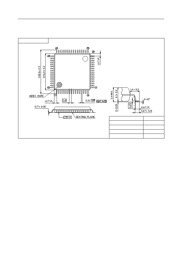
MSM9810
(Unit : mm)
PACKAGE DIMENSIONS
Notes for Mounting the Surface Mount Type Package
The SOP, QFP, TSOP, SOJ, QFJ (PLCC), SHP and BGA are surface mount type packages, which
are very susceptible to heat in reflow mounting and humidity absorbed in storage.
Therefore, before you perform reflow mounting, contact Oki's responsible sales person for the
product name, package name, pin number, package code and desired mounting conditions
(reflow method, temperature and times).
QFP64-P-1414-0.80-BK
Package material
Lead frame material
Pin treatment
Solder plate thickness
Package weight (g)
Epoxy resin
42 alloy
Solder plating
5 mm or more
0.87 TYP.
Mirror finish

NOTICE
1.
The information contained herein can change without notice owing to product and/or
technical improvements. Before using the product, please make sure that the information
being referred to is up-to-date.
2.
The outline of action and examples for application circuits described herein have been
chosen as an explanation for the standard action and performance of the product. When
planning to use the product, please ensure that the external conditions are reflected in the
actual circuit, assembly, and program designs.
3.
When designing your product, please use our product below the specified maximum
ratings and within the specified operating ranges including, but not limited to, operating
voltage, power dissipation, and operating temperature.
4.
Oki assumes no responsibility or liability whatsoever for any failure or unusual or
unexpected operation resulting from misuse, neglect, improper installation, repair, alteration
or accident, improper handling, or unusual physical or electrical stress including, but not
limited to, exposure to parameters beyond the specified maximum ratings or operation
outside the specified operating range.
5.
Neither indemnity against nor license of a third party's industrial and intellectual property
right, etc. is granted by us in connection with the use of the product and/or the information
and drawings contained herein. No responsibility is assumed by us for any infringement
of a third party's right which may result from the use thereof.
6.
The products listed in this document are intended for use in general electronics equipment
for commercial applications (e.g., office automation, communication equipment,
measurement equipment, consumer electronics, etc.). These products are not authorized
for use in any system or application that requires special or enhanced quality and reliability
characteristics nor in any system or application where the failure of such system or
application may result in the loss or damage of property, or death or injury to humans.
Such applications include, but are not limited to, traffic and automotive equipment, safety
devices, aerospace equipment, nuclear power control, medical equipment, and life-support
systems.
7.
Certain products in this document may need government approval before they can be
exported to particular countries. The purchaser assumes the responsibility of determining
the legality of export of these products and will take appropriate and necessary steps at their
own expense for these.
8.
No part of the contents contained herein may be reprinted or reproduced without our prior
permission.
9.
MS-DOS is a registered trademark of Microsoft Corporation.
Copyright 1999 Oki Electric Industry Co., Ltd.
Printed in Japan
E2Y0002-29-62