 | –≠–ª–µ–∫—Ç—Ä–æ–Ω–Ω—ã–π –∫–æ–º–ø–æ–Ω–µ–Ω—Ç: MSM9844GA | –°–∫–∞—á–∞—Ç—å:  PDF PDF  ZIP ZIP |

° Semiconductor
VOICE SYNTHESIS LSI with on-chip FIFO Memory
MSM9844
Version1.20, Jun.16, 1999
Page1
∑
∑
∑
∑
∑
General Description
∑
∑
∑
∑
∑
Features
MSM9844 is a Voice Synthesizer LSI with on-chip FIFO memory.
A newly developed synthesis algorithm, OKI ADPCM2, promises superb sound quality. The LSI is fully
controllable from an external CPU via 16/8-bit bus interface.
MSM9844 is an ideal choice for application systems where such non-microchip data storage as CD ROM is
used..
∑ 16/8-bit Bus Interface
∑ On-chip FIFO Memory Capacity : 1024 Bits 23 ms Buffering
When Sampling Frequency at 8.0 kHz, 4-bit ADPCM and Monaural Playback selected
∑ Synthesis Algorithms for User's Selection
4,5,6,7,8-bit OKI ADPCM2
4-bit OKI ADPCM
8/16-bit Straight PCM
8-bit OKI Non-Linear PCM
∑ Oscillation Clock Frequency: 16.9344 MHz / 24.576 MHz
∑ Sampling Frequency:
11.025 kHz, 22.05 kHz, 44.1 kHz at f
OSC
=16.9344 MHz
4.0 kHz, 6.4 kHz, 8.0 kHz, 12.8 kHz, 16.0 kHz, 32.0 kHz, 48.0 kHz at f
OSC
=24.576 MHz
∑ Sound Level Control (8 levels, 0dB ~ -21dB)
∑ Built-in 14-bit D/A Converter
∑ 3 types of Serial Interface for External DAC
∑ Sampling Rate Conversion Function
∑ Packaging: 56-pin Plastic QFP (QFP56-P-910-0.65-2K)
Product Code: MSM9844GA

Page2
° Semiconductor
MSM9844
∑
∑
∑
∑
∑
Pin Layout (Top View)
56-pin Plastic QFP
D0
D9
D11
D2
D3
D5
D4
D6
D7
D10
D8
D1
DV
DD
NC
1
12
14
3
4
7
6
8
9
13
11
2
5
10
BUSY
DV
DD
AOUTR
CS
RD
MID
FUL / DREQR
EMP
CH / DACKR
AV
DD
CBUSY
D / C
WR
RESET
42
31
29
40
39
36
37
35
34
30
32
41
38
33
NC
TEST2
SIOCK
XT
NC
DACKL
DREQL
DGND
TEST1
DASD
VCK
XT
IOW
TEST0
56
45
43
54
53
50
51
49
48
44
46
55
52
47
NC
TEST3
AOUTL
D13
D14
DGND
NC
AGND
NC
NC
NC
D12
D15
NC
15
26
28
17
18
21
20
22
23
27
25
16
19
24

Page3
° Semiconductor
MSM9844
∑
∑
∑
∑
∑
Block Diagram
EMP
MID
FUL/DREQR
CH/DACKR
D15 to D0
WR
RD
CS
D / C
BUSY
CBUSY
AV
DD
AGND
DV
DD
DGND
VCK
SIOCK
DASD
DREQL
DACKL
TEST0
TEST1
IOW
XT
XT
RESET
AOUTL
AOUTR
FIFO
MCU
I / F
DMA I / F
Timing Controller
Serial Port
ADPCM2 / ADPCM / PCM
Synthesizer
Volume Controller
DAC
DAC
LPF
LPF

Page4
° Semiconductor
MSM9844
∑
∑
∑
∑
∑
Pin Description
When 8-bit bus interface selected, you can define, by using a command,
these pins as input/output to/from external memory. When no definition
made, these pins are output mode.
When 16-bit bus interface selected, they are one half of bi-directional data
bus for data input / output from/to external micro-controller and memory.
Another half of bi-directional data bus for data input/output from/to external
micro-controller and memory and for status output.
WRITE pulse input pin. Input "L" pulse before you can enter command
and data to D15 to D0 pins.
READ pulse input pin. Input "L" pulse before the LSI can output status and
data to D15 to D0 pins.
With this pin at "L" level, the LSI accepts WRITE or READ pulse input. At
"H" level the LSI would not accept WRITE or READ pulse.
While this pin being held "H", D15 to D0 pins are enabled to input/output
sound data. While this pin being held "L", D7 to D0 pins are enabled to
input a command or output status data.
Output "L" level during playback/PAUSE operation.
Output "L" level when the LSI is ready to accept a command.
"H" level output from this pin indicates FIFO memory is empty. You can
change this pin to "L" active by a command input.
"H" level output from this pin indicates FIFO memory is more than half.
During playback, voice synthesis starts when MID changes to "H" level.
You can change this pin to "L" active by a command input. This pin
outputs a synchro signal for voice data input / output when non-use of FIFO
is selected.
"H" level output from this pin indicates FIFO memory is full. During
playback operation this pin is held "H" and FIFO memory is write -disabled.
You can change this pin to "L" active by a command input.
When DMA Transfer and stereo-playback selected by the command input,
the output from this pin becomes DMA Transfer request signal. The pin
outputs "H" when the right channel FIFO memory is empty. You can
change this pin to "L" active by a command input.
When stereo-playback selected, write sound data to the right channel FIFO
at "H" level, while data to the left channel FIFO at "L" level. When monaural
playback selected, keep this pin "L". You can change this pin to "L" active by
a command input.
When DMA Transfer and stereo-playback selected by the command input,
this pin acknowledges the right channel DMA Transfer permission signal.
With this pin at "L" level the LSI enabled the /IOW pin to accept the signal.
You can change this pin to "H" active by a command input.
Output "H" level to represent DMA Transfer request signal when FIFO gets
empty. If stereo-playback selected, the pin outputs "H" level to represent
DMA Transfer request signal when the left channel FIFO gets empty.
DMA Transfer Permission Acknowledgement signal. With this pin at "L"
level the LSI enables the /IOW pin to accept the signal. When stereo-
playback selected, the pin acknowledges DMA Transfer permission signal
for the left channel FIFO. You can change this pin to "H" active by a
command input. When DMA Transfer is not in use, keep the pin "H".
Pin No.
Symbol
I / O
Description
I / O
I / O
I
I
I
I
O
O
O
O
I
O
I
D15 to D8
D7 to D0
WR
RD
CS
D / C
BUSY
CBUSY
EMP
FUL /
DREQR
CH /
DACKR
DREQL
DACKL
11 - 14
16 - 19
1 - 4
6 - 9
38
39
40
41
42
32
35
37
34
51
50
O
MID
36

Page5
° Semiconductor
MSM9844
When DMA Transfer selected, the signal to start writing external memory
data to the MSM9844 is entered to this pin.
When DMA Transfer is not use, keep the pin "H".
16-bit serial data output pin when the external DAC is in use.
Synchronizing clock signal for 16-bit serial data input/output when the
external DAC is in use.
Pins wired to the oscillator, When the external clock is used, input the
clock signal to the XT pin and keep the /XT pin open.
Input/Output the sampling frequency in use. The signal is used as the
synchronizing signal when the external DAC is in use.
"L" level input to this pin turns the LSI to the initial status.
Pins for testing the LSI. Keep these pins "L".
The left channel output from the built-in LPF. Analog waveform output can
be directly connected to an amplifirer to drive a speaker.
The right channel output from the built-in LPF. Analog waveform output can
be directly connected to an amplifirer to drive a speaker.
Digital power supply pin. Insert a 0.1µF or larger bypass capacitor
between this pin and the DGND pin.
Digital GND pin.
Analog power supply pin. Insert a 0.1µF or larger bypass capacitor
between this pin and the AGND pin.
Analog GND pin.
Pin No.
Symbol
I / O
Description
I
O
I / O
I
O
I / O
I
I
O
O
IOW
SIOCK
DASD
XT
XT
VCK
RESET
TEST0,1
TEST2,3
AOUTL
AOUTR
DV
DD
AV
DD
AGND
DGND
52
43
44
54
55
46
33
47,48
45,26
28
29
31
30
22
21,49

Page6
° Semiconductor
∑
∑
∑
∑
∑
Absolute Maximum Ratings
∑
∑
∑
∑
∑
Recommended Operating Ranges
∑
∑
∑
∑
∑
DC Characteristics
MSM9844
Parameter
Power Supply Voltage
Conditions
T
STG
V
IN
V
DD
Symbol
Storage Temperature
- 0.3 to V
DD
+ 0.3
- 0.3 to + 7.0
Unit
Rating
Ta = 25∞C
- 55 to + 150
V
V
∞C
Input Voltage
(GND = 0 V)
Parameter
Power Supply Voltage
Conditions
f
OSC
T
OP
V
DD
Symbol
Master Clock Frequency
- 40 to + 85
+ 4.5 to + 5.5
Unit
Rating
24.576
∞C
V
MHz
Operating Temperature
(GND = 0 V)
DGND = AGND = 0V
Parameter
"H" Input Voltage
Conditions
V
IH
Symbol
Unit
Min.
V
V
"H" Output Voltage note 1
DV
DD
= AV
DD
= + 4.5 V to + 5.5 V
DGND = AGND = 0 VTa = - 40 to + 85 ∞C
V
Max.
Typ.
V
DD
x 0.85
note 1) Applies to output pins excluding XT pin.
note 2) Applies to XT pin.
note 3) Applies to input pins excluding XT pin.
note 4) Applies to XT pins .
note 5) Applies to input pins without pull-up-register excluding XT pin.
note 6) Applies to input pins within pull-up-register excluding XT pin.
V
IL
"L" Input Voltage
"L" Output Voltage note 1
"H" Input Current note 3
"H" Input Current note 4
"L" Input Current note 5
"L" Input Current note 4
"L" Input Current note 6
Operating Current Consumption
Standby Current Consumption
I
IH2
V
OL1
IIH1
V
OH1
IIL1
IIL2
IIL3
IDD
IDDS
I
OH = - 40 µA
I
OL = 2 mA
V
IH =
V
DD
V
IH =
V
DD
V
IL =
GND
V
IL =
GND
V
IL =
GND
f
OSC =
24.576 MHz
without load
At power down
without load
Ta = - 40 to + 70 ∞C
At power down
without load
Ta = - 40 to + 85 ∞C
V
DD
x 0.15
V
DD
- 0.3
0.45
10
20
- 10
- 20
- 400
- 20
40
2 mA
2 mA
µA
V
µA
µA
µA
µA
mA
µA
µA
10
50
V
"H" Output Voltage note 2
"L" Output Voltage note 2
V
OL2
V
OH2
I
OH = - 40 µA
I
OL = 2 mA
V
DD
- 0.3
0.8
V

Page7
° Semiconductor
∑
∑
∑
∑
∑
AC Characteristics
MSM9844
Parameter
RESET Pulse Width
t
RSTW
Symbol
Unit
Min.
µs
ns
DV
DD
= AV
DD
= + 4.5 V to + 5.5 V
DGND = AGND = 0 VTa = - 40 to + 85 ∞C
ns
Max.
Typ.
t
RSTD
Setup Time after Rise of Power Supply for Fall of RESET
t
DRE
t
RR
t
CR
t
RSTS
t
DRF
t
CRC
t
WW
t
CW
120
500
160
ns
ns
ns
ns
ns
ns
Time to Active First RD, WR after Fall of RESET
RD Pulse Width
CS, D/C, CH Setup and Hold Time for RD
Time from Fall of RD till Data and Status Definition
Time from Fall of RD till Data Float
Time from Rise of RD till Fall of Next RD
IOW Pulse Width
WR Pulse Width
CS, D/C, CH Setup and Hold Time for WR
Setup Time of Data, and Command for Rise of WR
Hold Time of Data, and Command for Rise of WR
Time from Rise of WR till Fall of Next WR
Setup and Hold Time of DACK for IOW
Setup Time of Data for Rise of IOW
Hold Time of Data for Rise of IOW
Time from Rise of IOW till Fall of Next IOW
t
DWS
t
DWH
t
CWC
t
IOWW
t
DW
t
IOWS
t
IOWH
t
IOWC
160
30
300
500
200
30
100
10
500
160
10
100
10
200
50
10
ns
ns
ns
ns
ns
ns
ns
ns
ns
∑
∑
∑
∑
∑
Analog Characteristics
Parameter
D/A Output Relative Error
Conditions
V
DAE
Symbol
Unit
Min.
mV
DV
DD
= AV
DD
= + 4.5 V to + 5.5 V
DGND = AGND = 0 VTa = - 40 to + 85 ∞C
Max.
Typ.
10
R
AOUT
AOUT Output Load Resistance
No Load
50
k

Page8
° Semiconductor
∑
∑
∑
∑
∑
Timing Chart
MSM9844
RESET Timing
V
DD
RESET (I)
RD or WR (I)
t
RSTD
t
RSTW
t
RSTS
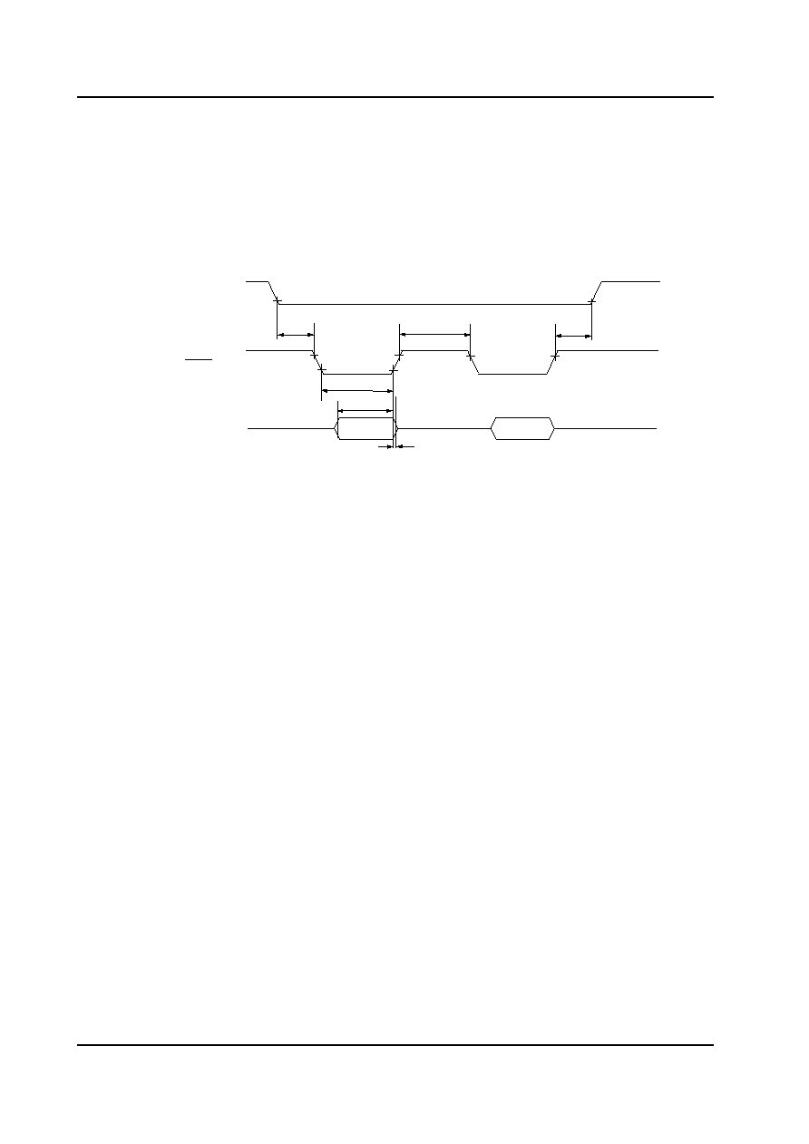
READ Timing Status READ
CS (I)
D / C (I)
RD (I)
D7 to D0 (I/O)
t
CR
t
CR
t
RR
t
DRE
t
DRF
Don't Care

Page9
° Semiconductor
MSM9844
WRITE Timing
(1) DATA WRITE
CS (I)
D / C (I)
WR (I)
D7 to D0 (I/O)
t
CW
t
CW
t
WW
t
DWS
t
DWH
Don't Care
CH (I)
(2) COMMAND WRITE
CS (I)
D / C (I)
WR (I)
D7 to D0 (I/O)
t
CW
t
CW
t
WW
t
DWS
t
DWH
Don't Care
(3) WRITE CYCLE
WR (I)
t
CWC
Page10
° Semiconductor
MSM9844
DMA Timing
IOW Timing (for Playback and Write 2 bytes DATA)
DACKL (I)
or DACLR (I)
D7 to D0 (I/O)
t
IOWW
IOW (I)
t
IOWC
t
DW
t
DW
t
IOWH
t
IOWS

Page11
° Semiconductor
MSM9844
Playback Timing with using External MCU and Memory
RESET (I)
MCU I/F
BUSY (O)
1
2
3
4
5
EMP (O)
MID (O)
FUL (O)
AOUT (O)
1/2 V
DD
Command Write Cycle
PLAY
Data Write Cycle
Output the last data
or Input STOP Command
End of Playback
Playback Timing with using DMA Controller
RESET (I)
MCU I/F
BUSY (O)
1
2
3
4
5
EMP (O)
MID (O)
FUL internal
AOUT (O)
1/2 V
DD
Command Write Cycle
PLAY
Data Write Cycle
No use CS,WR, and RD pins
Output the last data
or Input STOP Command
End of Playback
DREQ (O)
DACK (I)
IOW (I)

∑
∑
∑
∑
∑
Functional Description
∑ Voice Synthesis Algorithms
To meet user's varying sound quality requirements, 4 different types of voice synthesis algorithms are
available for user's selection as follows:
1. OKI 4-bit ADPCM
2. OKI 4/5/6/7/8-bit ADPCM2
3. 8/16-bit Straight PCM
4. 8-bit Non-linear PCM
Page12
° Semiconductor
MSM9844
∑ Data Formats When 8-bit Bus Selected
1. Oki 4-bit ADPCM, Oki 4-bit ADPCM2
2. Oki 5-bit ADPCM2
3. Oki 6-bit ADPCM2
4. Oki 7-bit ADPCM2
5. Oki 8-bit ADPCM2, 8-bit Linear PCM, and 8-bit Oki Non-Linear PCM
6. 16-bit Linear PCM
D7
MSB1
MSB3
D6
3SB1
3SB3
D5
2SB1
2SB3
D4
LSB1
LSB3
D3
MSB2
MSB4
D2
3SB2
3SB4
D1
2SB2
2SB4
D0
LSB2
LSB4
D7
X
X
D6
X
X
D5
X
X
D4
MSB1
MSB2
D3
4SB1
4SB2
D2
3SB1
3SB2
D1
2SB1
2SB2
D0
LSB1
LSB2
D7
X
X
D6
X
X
D5
MSB1
MSB2
D4
5SB1
5SB2
D3
4SB1
4SB2
D2
3SB1
3SB2
D1
2SB1
2SB2
D0
LSB1
LSB2
D7
X
X
D6
MSB1
MSB2
D5
6SB1
6SB2
D4
5SB1
5SB2
D3
4SB1
4SB2
D2
3SB1
3SB2
D1
2SB1
2SB2
D0
LSB1
LSB2
D7
MSB1
MSB2
D6
7SB1
7SB2
D5
6SB1
6SB2
D4
5SB1
5SB2
D3
4SB1
4SB2
D2
3SB1
3SB2
D1
2SB1
2SB2
D0
LSB1
LSB2
D7
MSB1
8SB1
D6
15SB1
7SB1
D5
14SB1
6SB1
D4
13SB1
5SB1
D3
12SB1
4SB1
D2
11SB1
3SB1
D1
10SB1
2SB1
D0
9SB1
LSB1

Page13
° Semiconductor
MSM9844
∑ Data Formats When 16-bit Bus Selected
1. Oki 4-bit ADPCM, Oki 4-bit ADPCM2
2. Oki 5-bit ADPCM2
3. Oki 6-bit ADPCM2
4. Oki 7-bit ADPCM2
5. Oki 8-bit ADPCM2, 8-bit Linear PCM, and 8-bit Oki Non-Linear PCM
6. 16-bit Linear PCM
D15
MSB1
D7
MSB3
D14
3SB1
D6
3SB3
D13
2SB1
D5
2SB3
D12
LSB1
D4
LSB3
D11
MSB2
D3
MSB4
D10
3SB2
D2
3SB4
D9
2SB2
D1
2SB4
D8
LSB2
D0
LSB4
D15
X
D7
X
D14
X
D6
X
D13
X
D5
X
D12
MSB1
D4
MSB2
D11
4SB1
D3
4SB2
D10
3SB1
D2
3SB2
D9
2SB1
D1
2SB2
D8
LSB1
D0
LSB2
D15
X
D7
X
D14
X
D6
X
D13
MSB1
D5
MSB2
D12
5SB1
D4
5SB2
D11
4SB1
D3
4SB2
D10
3SB1
D2
3SB2
D9
2SB1
D1
2SB2
D8
LSB1
D0
LSB2
D15
X
D7
X
D14
MSB1
D6
MSB2
D13
6SB1
D5
6SB2
D12
5SB1
D4
5SB2
D11
4SB1
D3
4SB2
D10
3SB1
D2
3SB2
D9
2SB1
D1
2SB2
D8
LSB1
D0
LSB2
D15
MSB1
D7
MSB2
D14
7SB1
D6
7SB2
D13
6SB1
D5
6SB2
D12
5SB1
D4
5SB2
D11
4SB1
D3
4SB2
D10
3SB1
D2
3SB2
D9
2SB1
D1
2SB2
D8
LSB1
D0
LSB2
D15
MSB1
D7
8SB1
D14
15SB1
D6
7SB1
D13
14SB1
D5
6SB1
D12
13SB1
D4
5SB1
D11
12SB1
D3
4SB1
D10
11SB1
D2
3SB1
D9
10SB1
D1
2SB1
D8
9SB1
D0
LSB1

Page14
° Semiconductor
MSM9844
∑ Playback Operation When Micro-controller Interface in Use
(1) Define a synthesis algorithm, sampling frequency, bus width, playback mode, and etc. as required, by
using an appropriate command.
(2) To start playback, input the PLAY command. Or, write one word data to FIFO, letting the LSI ready for
playback, and turn the EMP pin to "L" to initiate playback.
(3) Status shifting indicated by the EMP and FUL pins
(EMP="L", MID="L", FUL="L")
Indicates the state where no one-word data is written to FIFO memory.
(EMP="H", MID="L", FUL="L")
Indicates the state where one-word or more data is written to FIFO memory.
(EMP="L", MID="H", FUL="L")
Indicates the state where data is written to more than half of FIFO memory.
(EMP="L", MID="H", FUL="H")
Indicates the state where FIFO memory is full.
(4) Ending playback
When a write cycle is not completed within pre-fixed time, the LSI deems it as a completed write cycle and
ends playback.
∑ FIFO Memory's Status Shift
: Empty Block
: Write Done Block
: Block Being Read
EMP=H
MID =L
FUL =L
EMP=L
MID =L
FUL =L
EMP=L
MID =H
FUL =L
EMP=L
MID =H
FUL =H
EMP=L
MID =L
FUL =L
EMP=L
MID =L
FUL =L
EMP=H
MID =L
FUL =L
Start Playback
Playing Back
End Playback

Page15
° Semiconductor
MSM9844
MSM9844 issues a DMA Transfer request to the DMA Controller, and starts data transfer in sync with
transfer cycles of the DMA Controller after acknowledging a DMA Transfer permission. Enable/Disable of
DMA Transfer function can be defined by using the command.
The DREQL pin rises to "H" at the Start Playback command, requesting a write cycle to FIFO memory, and
maintains "H" level until FIFO gets full.
At the point of time when one-word data is written to FIFO, playback starts. When FIFO becomes half, the
DREQL returns to "H".
<DACKL Pin>
The pin is able to acknowledge a DMA Transfer permission signal from the DMA Controller. The /IOW pin
is enabled with the /DACKL pin at "L".
During the period of /DACKL="L" , controls using the /RD, /WR, CS, D/C pins are disabled. Therefore,
setups of MSM9844 has to be completed before you can enter into a DMA Transfer cycle.
</IOW Pin>
The pin is enabled at /DACKL="L", and thereafter controlled by the DMA Controller. The /IOW is an input pin
to enable data transfer from external memory to the MSM9844.
You can suspend on-going playback by using the Pause command. At this time, you may suspend Write
operation to FIFO memory while in pause. Write is resumed from where having been paused, when
playback restarts.
Or, you may continue Write operation to FIFO memory according to the EMP, MID and FUL pins' status.
You can stop on-going playback by using the STOP command. When this happens, FIFO memory is
cleared to return to the initial status.
∑Playback Operation When DMA Interface in Use
∑Pausing Playback
∑Stopping On-going Playback

Page16
° Semiconductor
MSM9844
You can select one of the following three types of serial interface by using the command.
1. MSB First (Master/Slave)
2. LSB First (Master/Slave)
3. IIS Format (Master/Slave)
∑Serial Port Data Format
(1) MSB 16 bit (J1 = 0, J0 = 0)
1 2 3 4 5 6 7 8 9 10111213141516 1 2 3 4 5 6 7 8 9 10111213141516
VCK
SIOCK
DASD
MSB
LSB MSB
LSB
LEFT
RIGHT
(2) LSB 16 bit (J1 = 0, J0 = 1)
1 2 3 4 5 6 7 8 9 10111213141516 1 2 3 4 5 6 7 8 9 10111213141516
VCK
SIOCK
DASD
LSB
MSB LSB
MSB
LEFT
RIGHT
(3) MSB, VCK Inverted, and DASD Shifted 1 bit16 bit (J1 = 1, J0 = 1)
1 2 3 4 5 6 7 8 9 10111213141516 1 2 3 4 5 6 7 8 9 10111213141516
VCK
SIOCK
DASD
MSB
LSB MSB
LSB
LEFT
RIGHT

Page17
° Semiconductor
MSM9844
∑ Sampling RATE Conversion
You can convert a sampling frequency for data output to another sampling frequency.
You can select an input sampling frequency with Sampling Rate Conversion Command and select SRC
available.
The SRC function supports only to convert monaural 44.1 kHz sampling. Select 26H data with PLAY
Command.
4.0, 6.4, 8.0, 12.8, 16.0kHz sampling frequencies are available to convert.
Master oscillation frequency is at 16.9344 MHz.

Page18
° Semiconductor
MSM9844
∑
∑
∑
∑
∑
Command Code Format
D7
D1
D2
D3
D4
D5
D6
D0
Function
0
X
X
X
0
0
0
X
0
L1
L2
L3
1
0
0
L0
0
S1
S2
H3
0
1
0
S0
0
X
C2
C3
1
1
0
X
0
C1
C2
C3
0
0
1
C0
0
V1
V2
H3
1
0
1
V0
0
X
W2
W3
0
1
1
X
0
P1
P2
P3
1
1
1
P0
1
R1
R2
R3
0
0
0
R0
1
1
0
0
1
0
1
0
1
1
1
0
1
0
0
1
1
1
0
1
1
0
1
1
E1
A2
A3
E0
B1
X
X
B0
D1
D2
F3
D0
G0
G1
G2
X
J1
X
I3
J0
X
X
X
X
NOP
Sampling RATE Conversion
PLAY
STOP
PAUSE
VOLUME
POWER DOWN
SELECT ALGORITHM
ANALOG SETUP 1
ANALOG SETUP 2, BUS WIDTH
DEFINE FIFO SIZE
SIGNAL OUTPUT FORMAT
SELECT DMA TRANSFER
SELECT Serial Port FORMAT
NOP
1
1
1
1
T1
T2
T3
T0
TEST
X = Don't Care

Page19
° Semiconductor
MSM9844
1) NOP Command
D7
D1
D2
D3
D4
D5
D6
D0
Function
0
X
X
X
0
0
0
X
NOP
NOP
1
X
X
X
0
1
1
X
No particular function
2) Sampling RATE Conversion Command
D7
D1
D2
D3
D4
D5
D6
D0
Function
0
L1
L2
L3
1
0
0
L0
Sampling RATE Conversion
By using this command you can select enable / disable Sampling Rate Conversion and input sampling
frequency when enable this function. Note that this command is enable with monaural playback.
Function
NOT used Sampling Rate Conversion *
Used Sampling Rate Conversion
* Default
L3
0
1
Sampling Frequency
0
0
0
0
0
1
1
0
0
1
0
1
0
1
0
0
1
1
1
1
0
1
1
1
L1
L2
L0
4.0 kHz
8.0 kHz
6.4 kHz
12.8 kHz
16.0 kHz

Page20
° Semiconductor
MSM9844
3) PLAY Command
D7
D1
D2
D3
D4
D5
D6
D0
Function
0
S1
S2
C3
0
1
0
S0
PLAY
To start playback, use this command. You can select either the left or right channel playback with C3, as
well as sampling frequency with S2 ~ S0. When stereo-playback is selected, data at C3 is disregarded. You
can select only one sampling frequency.
When the rate converter is used, the frequency defined by S2 ~ S0 is output sampling frequency.
Function
PLAY LEFT *
PLAY RIGHT
* Default
C3
0
1
XT = 16.9344MHz
0
0
0
11.025 kHz *
0
0
1
22.05 kHz
1
0
0
1
0
1
0
1
0
0
1
1
1
1
0
1
1
1
S1
S2
S0
Sampling Frequency
XT = 24.576MHz
16.0 kHz *
32.0 kHz
44.1 kHz
4.0 kHz
8.0 kHz
6.4 kHz
12.8kHz
48.0 kHz
2.76 kHz
5.51 kHz
4.41 kHz
8.82 kHz
* Default

Page21
° Semiconductor
MSM9844
4) STOP Command
D7
D1
D2
D3
D4
D5
D6
D0
Function
0
X
C2
C3
1
1
0
X
STOP
Use this command to stop playback. After the command input, FIFO data is cleared. C3 allows you to
select the left channel or the right channel playback to be stopped. When you want to stop playback on both
channels, use C2.
C2
Function
0
STOP LEFT *
0
STOP RIGHT
* Default
C3
0
1
1
STOP LEFT and RIGHT
X
5) PAUSE Command
D7
D1
D2
D3
D4
D5
D6
D0
Function
0
C1
C2
C3
0
0
1
X
PAUSE
Use this command to temporarily suspend on-going playback. C1 enables you to control PAUSE/reset.
You can select either the left channel or right channel with C3. When you want to suspend playback on both
channels, use C2.
C2
Function
0
PAUSE LEFT *
0
PAUSE RIGHT
* Default
C3
0
1
1
PAUSE LEFT and RIGHT
X
Function
PAUSE
RESUME
C1
0
1

Page22
° Semiconductor
MSM9844
6) VOLUME Command
D7
D1
D2
D3
D4
D5
D6
D0
Function
0
V1
V2
C3
1
0
1
V0
VOLUME
You can control sound level of playback by using this command. C3 is to select either the left channel or
right channel, and V2 ~ V0 is to select a proper sound level.
Function
LEFT VOLUME CONTROLL
RIGHT VOLUME CONTROLL
C3
0
1
1
VOL.VALUE
0
0
0
0 dB *
0
0
1
- 3 dB
1
0
0
1
0
1
0
1
0
0
1
1
1
1
0
1
1
1
V1
V2
V0
- 6 dB
- 9 dB
- 12 dB
- 15 dB
- 18 dB
- 21 dB
* Default
7) POWER DOWN Command
D7
D1
D2
D3
D4
D5
D6
D0
Function
0
X
W2
W3
0
1
1
X
POWER DOWN
Inputting this command puts the LSI into power down status, where the LSI stops oscillation and minimize
power consumption. Output from the AOUTL and AOUTR dropped down to the GND level instantaneously.
W3 enables you to control power down/reset and W2 to define whether initialize the LSI or not.
Function
RESUME POWER DOWN
POWER DOWN
W3
0
1
1
Function
NOT initialize the LSI
Initialize the LSI
W2
0
1
1

Page23
° Semiconductor
MSM9844
8) Select Algorithm Command
D7
D1
D2
D3
D4
D5
D6
D0
Function
0
P1
P2
P3
1
1
1
P0
SELECT ALGORITHM
You can select a voice synthesis algorithm with this command. You can select one out of ten listed below
with P3 ~ P0.
You cannot change the algorithm during playback operation.
Algorithm
0
0
0
0
0
1
4bit ADPCM2 *
1
0
0
1
0
1
0
1
0
0
1
1
1
1
0
1
1
1
P1
P2
P0
5bit ADPCM2
6bit ADPCM2
7bit ADPCM2
8bit ADPCM2
4bit ADPCM
8bit Linear PCM
* Default
0
0
0
0
0
0
0
0
P3
0
0
0
8bit Non-Linear PCM
1
0
0
1
16bit Linear PCM
1

Page24
° Semiconductor
MSM9844
9) Analog Setup 1 Command
D7
D1
D2
D3
D4
D5
D6
D0
Function
1
R1
R2
R3
0
0
0
R0
ANALOG SETUP 1
This command allows you to select either internal/external DAC to be used, binary or two's compliment and
stereo or monaural for playback.
At powering up, output from the AOUTL and AOUTR pins rises to 1/2 VDD level instantaneously, disregard-
ing the setup value at R0.
Function
2's Complimentary Binary *
Binary
R3
0
1
1
Function
INTERNAL D/A C *
EXTERNAL D/A C
R2
0
1
1
Function
No particular function
R1
X
Function
Monaural PLAYBACK *
Stereo PLAYBACK
R0
0
1
1
* Default

Page25
° Semiconductor
MSM9844
10) Analog Setup 2 Command
D7
D1
D2
D3
D4
D5
D6
D0
Function
1
E1
A2
A3
1
0
0
E0
ANALOG SETUP 2
You can select enable/disable driving amplifier and enable/ disable LPF for the AOUTL and AOUTR pins
with A3 and A2.
You can also select a data bus width with E1 and E0, and when 8-bit bus selected, you can further select
whether to use D15 ~ D8 pins for sound data transfer.
Function
USED Output Amplifire *
NOT USED Output Amplifire
A3
0
1
1
Function
USED internal LPF *
NOT USED intrenal LPF
A2
0
1
1
E1
0
Function
8bit BUS Width, D15 to D8 unused *
E0
0
X
* Default
0
1
1
8bit BUS Width, D15 to D8 used
16bit BUS Width
11) Define FIFO Size Command
D7
D1
D2
D3
D4
D5
D6
D0
Function
1
B1
X
X
0
1
0
B0
DEFINE FIFO SIZE
By using this command you can define the size of FIFO memory.
8bit BUS Width
0
0
128 bytes
0
1
64 bytes
1
0
1
1
B1
B0
32 bytes
NOT USED FIFO Memory
16bit BUS Width
64 words
32 words
16 words

Page26
° Semiconductor
MSM9844
12) Signal Output Format Command
D7
D1
D2
D3
D4
D5
D6
D0
Function
1
D1
D2
F3
1
1
0
D0
SIGNAL OUTPUT FORMAT
By using this command you can select output format from the EMP, FUL and DREQL/R pins, and input
format to the DACKL/R pins.
Function
"H" Active for EMP, MID, and FUL Output *
"L" Active for EMP, MID, and FUL Output
F3
0
1
1
Function
"H" Active for DREQL, and DREQR Output *
"L" Active for DREQL, and DREQR Output
D2
0
1
1
Function
No particular function
NOT USED
D0
0
1
1
* Default
Function
"L" Active for DACKL, and DACKR Input *
"H" Active for DACKL, and DACKR Input
D1
0
1
1
13) Select DMA Transfer Command
D7
D1
D2
D3
D4
D5
D6
D0
Function
1
G1
G2
G3
0
0
1
X
SELECT DMA TRANSFER
By using this command you can select enable/disable DMA Transfer and DMA Transfer mode.
Function
X
0
X
Not used DMA Transfer *
0
1
0
DMA Transfer by Single Mode
0
1
1
G2
G3
G1
DMA Transfer by Block Mode
* Default

Page27
° Semiconductor
MSM9844
14) Select Serial Port Data Format Command
D7
D1
D2
D3
D4
D5
D6
D0
Function
1
J1
X
I3
1
0
1
J0
SELECT PORT DATA FORMAT
By using this command you can select a data format for the Serial Port.
Note that this command is valid only when R2 value of the Analog Setup 1 command is set to "1"
Function
VCK, SIOCK Master Mode *
VCK, SIOCK Slave Mode
I3
0
1
Function
MSB First, 16 bit(Mode 1) *
LSB First
J1
0
0
* Default
J0
0
1
I IS FORMAT, 16bit(Mode2)
1
1
0
1

Page28
° Semiconductor
MSM9844
15) Test Command
D7
D1
D2
D3
D4
D5
D6
D0
Function
1
T1
T2
T3
1
1
1
T0
TEST
This command is used only for testing the LSI. You are not allowed to use the command.
16) Status Read
Status
D7
D6
D5
D4
D3
D2
D1
D0
Pin Name
Pausing Lch
Pausing Rch
FIFO EMP Signal
FIFO MID Signal
During Playback Lch
FIFO FUL Signal
Data is writen to FIFO at FUL status
During Playback Rch
You can monitor the MSM9844 internal status with read-out data from D7 to D0.
The table shows the each status from D7 to D0.

Page29
° Semiconductor
MSM9844
∑ The Internal LPF Characteristics for AOUTL and AOUTR pins
There are two LPFs on MSM9844, which is consisted of Digital Filter Technology.
Figure shows each Frequency Characteristics of internal LPFs when the sampling frequency is at 8kHz
and 16kHz.
Frequency Characteristics of internal LPF at 8kHz sampling Frequency.
-100
-90
-80
-70
-60
-50
-40
-30
-20
-10
0
100
1000
10000
100000
Hz
dB
-100
-90
-80
-70
-60
-50
-40
-30
-20
-10
0
100
1000
10000
100000
Hz
dB
Frequency Characteristics of internal LPF at 16kHz sampling Frequency.

Page30
° Semiconductor
MSM9844
∑
∑
∑
∑
∑
Application Circuit Sample
D15 to D0
DREQL
DACKL
IOW
DREQR
DACKR
RD
WR
CS
D / C
MSM9844
MEMORY
DMA Controller
CPU or MCU
D15 to D0
RD
WR
CS
D / C
MSM9844
MEMORY
CPU or MCU
Sample 1 for interface with DMA Controller
Sample 2 for interface with External Memory
Data Bus
Data Bus
EMP
MID
FUL

Page31
° Semiconductor
MSM9844
Mirror finish
Package material
Lead frame material
Pin treatment
Solder plate thickness
Package weight (g)
Epoxy resin
42 alloy
Solder plating
5µm or more
0.43 TYP.
QFP56-P-910-0.65-2K
Notes for Mounting the Surface Mount Type Package
The SOP, QFP, TSOP, SOJ, QFJ (PLCC), SHP and BGA are surface mount type packages, which
are very susceptible to heat in reflow mounting and humidity absorbed in storage.
Therefore, before you perform reflow mounting, contact Oki's responsible sales person for the
product name, package name, pin number, package code, and desired mounting conditions
(reflow method, temperature and times).
∑
∑
∑
∑
∑
Package Dimensions
(Unit : mm)
(Unit : mm)
(Unit : mm)
(Unit : mm)
(Unit : mm)

Page32
° Semiconductor
MSM9844
NOTICE
1. The information contained herein can change without notice owing to product and/or technical
improvements. Before using the product, please make sure that the information being referred to is up-to-
date.
2. The outline of action and examples for application circuits described herein have been chosen as an
explanation for the standard action and performance of the product. When planning to use the product,
please ensure that the external conditions are reflected in the actual circuit and assembly designs.
3. When designing your product, please use our product below the specified maximum ratings and within
the specified operating ranges including, but not limited to, operating voltage, power dissipation, and
operating temperature.
4. OKI assumes no responsibility or liability whatsoever for any failure or unusual or unexpected operation
resulting from misuse, neglect, improper installation, repair, alteration or accident, improper handling, or
unusual physical or electrical stress including, but not limited to, exposure to parameters beyond the
specified maximum ratings or operation outside the specified operating range.
5. Neither indemnity against nor license of a third party's industrial and intellectual property right, etc. is
granted by us in connection with the use of product and/or the information and drawings contained
herein. No responsibility is assumed by us for any infringement of a third party's right which may result
from the use thereof.
6. The products listed in this document are intended for use in general electronics equipment for
commercial applications (e.g. office automation, communication equipment, measurement equipment,
consumer electronics ,etc.). These products are not authorized for use in any system or application that
requires special or enhanced quality and reliability characteristics nor in any system or application where
the failure of such system or application may result in the loss or damage of property, or death or injury to
humans. Such applications include, but are not limited to: traffic control, automotive, safety, aerospace,
nuclear power control, and medical, including life support and maintenance.
7. Certain products in this document may need government approval before they can be exported to
particular countries. The purchaser assumes the responsibility of determining the legality of export of these
products and will take appropriate and necessary steps at their own expense for these.
8. No part of the contents contained herein may be reprinted or reproduced without our prior permission.
9. MS-DOS is a registered trademark of Microsoft Corporation.
Copyright 1999 Oki Electric Industry Co.,Ltd.