
° Semiconductor
MSM9892L
1/6
° Semiconductor
MSM9892L
2M-bit Serial Voice Flash Memory
GENERAL DESCRIPTION
The MSM 9892L is a 2Mb flash memory that operates at 2.7 V to 3.6 V. Since backup is not needed,
the number of pins is small, and the pins are contained in a small-package 28-pin TSOP, the
MSM9892L is a flash memory suitable for applications such as handy terminals. In combination
with OKI's recording/playback IC (MSM9888L), a solid-state recording/playback system can be
easily constructed.
FEATURES
∑ Configuration
: 1024 pages • 2112 bits
∑ Small page size
: 2048 per page
(one time write unit)
∑ Power supply voltage : Single 2.7 to 3.6 V
∑ Operating current
: Supply current : Up to 35 mA
: Stanby current : Up to 10 mA
∑ Operating temperature : ≠10 to +70
∞
C
∑ Package:
28-pin plastic TSOP (TSOPI28-P-813-0.55-K) (Product name: MSM9892LTS-KT)
PIN CONFIGURATION
E2D0090-29-22
NC: No connection
28-Pin Plastic TSOP
TEST
1
28 NC
RESET 2
27 NC
PRT 3
26 NC
NC
4
25 NC
NC
5
24 NC
V
DD
6
23 NC
GND
7
22 NC
NC
8
21 NC
NC
9
20 NC
NC 10
19 NC
CS 11
18 NC
SCK 12
17 NC
DI 13
16 NC
DO 14
15 NC
This version: Feb. 1999
Previous version: May 1997

° Semiconductor
MSM9892L
2/6
PIN DESCRIPTIONS
Pin
Symbol
I/O
Description
13
DI
I
Command, address, or data input pin.
14
DO
O
Data output pin.
12
SCK
I
Inputs the data transfer clock for the DI and DO pins.
11
CS
I
The device accepts the SCK pulse when CS is at "L" level and does not accept the
SCK pulse when CS is at "H" level.
1
TEST
O
Output pin for test. Leave this pin open.
3
PRT
I
Prohibits flash memory programming when PRT is at "L" level.
2
RESET
I
The device is reset when RESET is at "L" level.
6
V
DD
I
Power supply pin (2.7 to 3.6 V)
7
GND
I
GND pin (0 V)
ABSOLUTE MAXIMUM RATINGS
Parameter
Symbol
Condition
Rating
Unit
Power Supply Voltage
V
DD
Ta=25∞C
≠0.3 to +7.0
V
Input Voltage
V
IN
≠0.6 to V
DD
+0.6
V
Storage Temperature
T
STG
--
≠55 to +150
∞C
RECOMMENDED OPERATING CONDITIONS
Parameter
Symbol
Condition
Range
Unit
Power Supply Voltage
V
DD
GND=0V
2.7 to 3.6
V
Operating Temperature
T
op
--
≠10 to +70
∞C
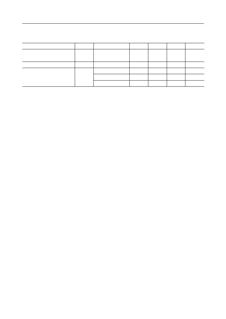
ELECTRICAL CHARACTERISTICS
DC Characteristics
Parameter
Symbol
Min.
Typ.
Max.
Unit.
Operating Current
Standby Current
"H" Input Voltage
"L" Input Voltage
"H" Output Voltage
"L" Output Voltage
Input Leakage current
Output Leakage current
I
CC
--
15
35
mA
I
SB
--
--
10
mA
V
IH
2.0
--
--
V
V
IL
--
--
0.6
V
V
OH
2.0
--
--
V
V
OL
--
--
0.4
V
I
IL
--
--
1
mA
I
OL
--
--
1
mA
Condition
--
T
op
=≠10 to +70
--
--
--
--
--
--
° Semiconductor
MSM9892L
3/6
PROGRAMMING/ERASE CHARACTERISTICS
Parameter
Programming/Erase Cycles
(per page)
Data Retention Time
Write Disturb *1)
Min.
Typ.
Max.
Unit
--
--
10,000
Cycles
per page
--
--
10
Years
--
--
50,000
Cycles
--
--
20,000
Cycles
--
--
100,000
Cycles
Symbol
C
EP
T
DR
C
PD
Condition
--
--
Bit error : 1bit
Bit error : None
Bit error : 3bits
*1)
"Write Disturb" means a phenomenon that frequent write operations performed to pages
in Flash memory may cause a data error in another page to which write operations are
not performed.
For example, 20,001 to 50,000 write operations performed onto pages other than page "n"
may cause a 1-bit error in page "n".
° Semiconductor
MSM9892L
4/6
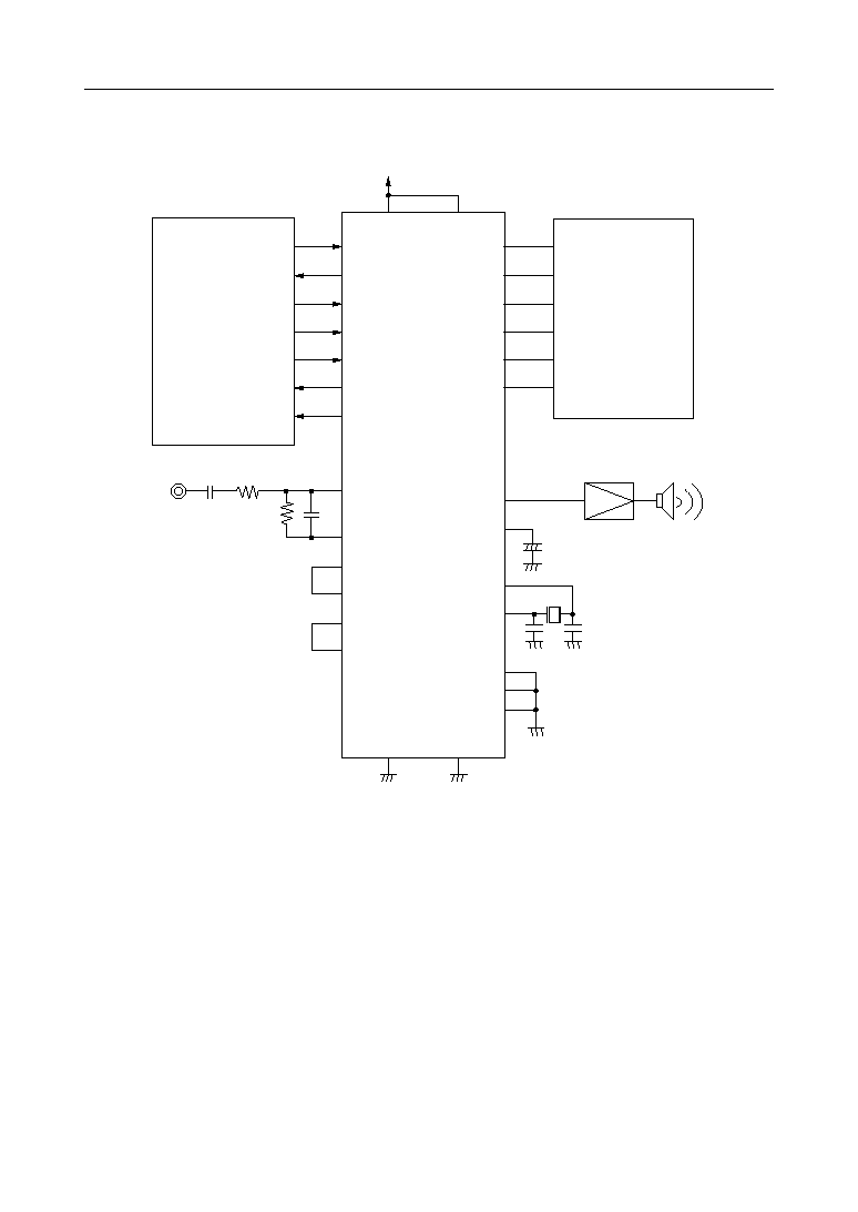
APPLICATION CIRCUIT
MSC1157
DI
DO
SCK
CS
RESET
PRT
MSM9892L
MSM9893L
MSM9894AL
DV
DD
AV
DD
DI
DO
SCK
CS
RESET
BUSY
MON
FDI
FDO
FSCK
FCS
FRESET
FPRT
MCU
Voice input
LIN
LOUT
AMON
FIN
FOUT
ADIN
AOUT
SG
XT
XT
TEST0
TEST1
TEST2
DGND
AGND
MSM9888L
+
° Semiconductor
MSM9892L
5/6
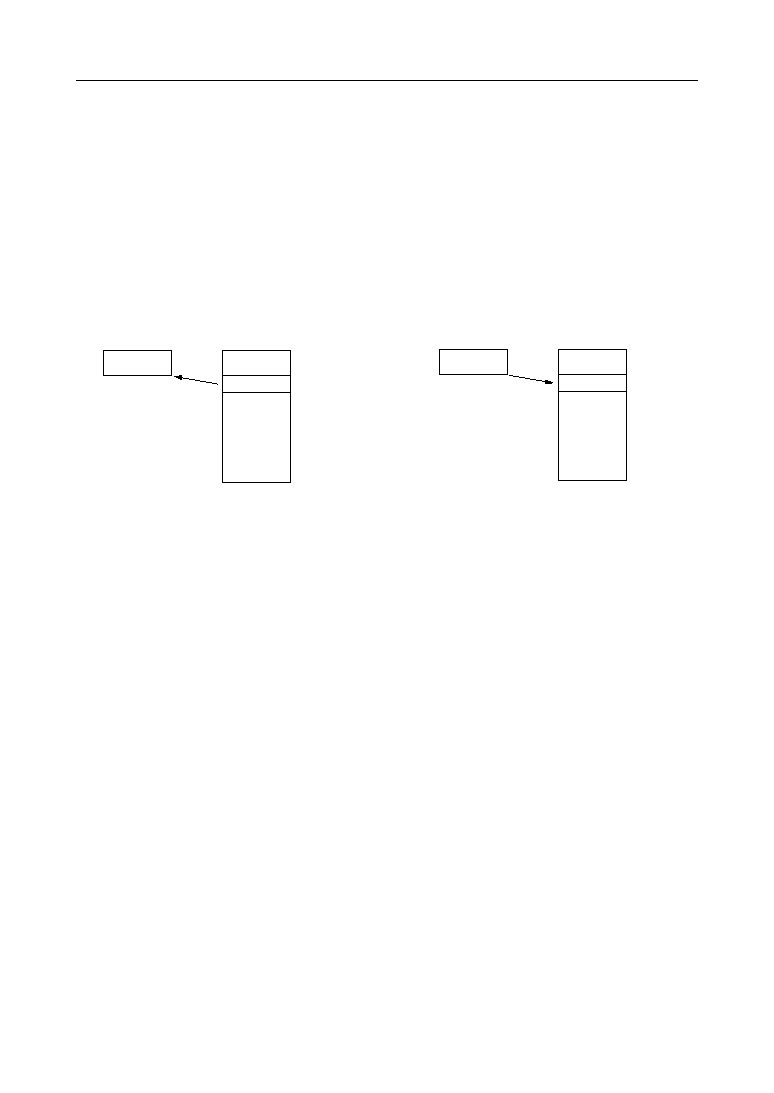
WRITE DISTURB
"Write Distrub" means a phenomenon that the change from digital "0" to "1" may occur in a Flash
memory page to which data is scarcely written.
The above change can be avoided by refreshing Flash memory data with the DTRW command
and WEND command of the MSM9888L/MSM9889L.
q DTRW command
This command moves some Flash memory
page data to buffer.
w WEND command
This command programs buffer data to
Flash memory.
TIMING WHEN POWER IS ON
Refer to the MSM9888L/MSM9889L Data Sheet. If the timing diagrams described in the
MSM9888L/MSM9889L Data Sheet are not satisfied, errors such as "Recording is disabled" or
"Recorded message is erased" may occur.
Flash
Buffer
Page "n"
Flash
Buffer
Page "n"

° Semiconductor
MSM9892L
6/6
(Unit : mm)
PACKAGE DIMENSIONS
Notes for Mounting the Surface Mount Type Package
The SOP, QFP, TSOP, TQFP, LQFP, SOJ, QFJ (PLCC), SHP, and BGA are surface mount type
packages, which are very susceptible to heat in reflow mounting and humidity absorbed in
storage. Therefore, before you perform reflow mounting, contact Oki's responsible sales person
on the product name, package name, pin number, package code and desired mounting conditions
(reflow method, temperature and times).
TSOP
I28-P-813-0.55-K
Package material
Lead frame material
Pin treatment
Solder plate thickness
Package weight (g)
Epoxy resin
42 alloy
Solder plating
7 mm or more
0.27 TYP.
MIRROR FINISH

NOTICE
1.
The information contained herein can change without notice owing to product and/or
technical improvements. Before using the product, please make sure that the information
being referred to is up-to-date.
2.
The outline of action and examples for application circuits described herein have been
chosen as an explanation for the standard action and performance of the product. When
planning to use the product, please ensure that the external conditions are reflected in the
actual circuit, assembly, and program designs.
3.
When designing your product, please use our product below the specified maximum
ratings and within the specified operating ranges including, but not limited to, operating
voltage, power dissipation, and operating temperature.
4.
Oki assumes no responsibility or liability whatsoever for any failure or unusual or
unexpected operation resulting from misuse, neglect, improper installation, repair, alteration
or accident, improper handling, or unusual physical or electrical stress including, but not
limited to, exposure to parameters beyond the specified maximum ratings or operation
outside the specified operating range.
5.
Neither indemnity against nor license of a third party's industrial and intellectual property
right, etc. is granted by us in connection with the use of the product and/or the information
and drawings contained herein. No responsibility is assumed by us for any infringement
of a third party's right which may result from the use thereof.
6.
The products listed in this document are intended for use in general electronics equipment
for commercial applications (e.g., office automation, communication equipment,
measurement equipment, consumer electronics, etc.). These products are not authorized
for use in any system or application that requires special or enhanced quality and reliability
characteristics nor in any system or application where the failure of such system or
application may result in the loss or damage of property, or death or injury to humans.
Such applications include, but are not limited to, traffic and automotive equipment, safety
devices, aerospace equipment, nuclear power control, medical equipment, and life-support
systems.
7.
Certain products in this document may need government approval before they can be
exported to particular countries. The purchaser assumes the responsibility of determining
the legality of export of these products and will take appropriate and necessary steps at their
own expense for these.
8.
No part of the contents cotained herein may be reprinted or reproduced without our prior
permission.
9.
MS-DOS is a registered trademark of Microsoft Corporation.
Copyright 1999 Oki Electric Industry Co., Ltd.
Printed in Japan
E2Y0002-29-11