 | –≠–ª–µ–∫—Ç—Ä–æ–Ω–Ω—ã–π –∫–æ–º–ø–æ–Ω–µ–Ω—Ç: MSM99QB22 | –°–∫–∞—á–∞—Ç—å:  PDF PDF  ZIP ZIP |

D
ATA
S
HEET
August 2002
O K I A S I C P R O D U C T S
MG73/74Q and MSM98Q/99Q
0.35µm Customer Structured Arrays

I
I
≠≠≠≠≠≠≠≠≠≠≠≠≠≠≠≠≠≠≠≠≠≠≠≠≠≠≠≠≠≠≠≠≠≠≠≠≠≠≠≠≠≠≠≠≠≠≠≠≠≠≠≠≠≠≠≠≠≠≠≠≠≠≠≠≠≠≠≠≠≠≠≠≠≠≠≠≠≠≠≠≠≠≠≠≠≠≠≠≠≠≠
Oki Semiconductor
CONTENTS
Description ................................................................................................................................................................1
Features ..................................................................................................................................................................... 1
MG73Q/74Q and MSM98Q/99Q Family Masterslices...................................................................................... 2
Array Architecture................................................................................................................................................... 3
CSA Layout Methodology .............................................................................................................................. 4
Electrical Characteristics ......................................................................................................................................... 5
Macro Library ........................................................................................................................................................... 8
Macrocells for Driving Clock Trees............................................................................................................... 9
Oki Advanced Design Center CAD Tools.......................................................................................................... 10
Oki Design Kit Availability .......................................................................................................................... 10
Design Process................................................................................................................................................ 11
Automatic Test Pattern Generation............................................................................................................. 12
Floorplanning Design Flow.......................................................................................................................... 12
IEEE JTAG Boundary Scan Support............................................................................................................ 13
Package Options..................................................................................................................................................... 14
1
Oki Semiconductor
MG73Q/74Q and MSM98Q/99Q
0.35µm Customer Structured Arrays
DESCRIPTION
Oki's 0.35µm Application-Specific Integrated Circuit (ASIC) products are available in Customer Struc-
tured Array (CSA) architectures with 0.60-µm or 100-µm I/O pad pitch. Both the MG73Q000 and the
MSM98Q000 series use a three-layer metal process on 0.35µm drawn (0.27µm L-effective) CMOS technol-
ogy. The MG74Q and MSM99Q series uses the same base-array architecture as the MG73Q or MSM99Q
series respectively, but offers four metal layers instead of three. The semiconductor process is adapted
from Oki's production-proven 64-Mbit DRAM manufacturing process.
The 0.35-µm family provides significant performance, density, and power improvement over previous
0.4 and 0.5µm technologies. The Oki 0.35-µm family operates using 3-V V
DD
core with optimized 3-V I/O
buffers and 3-V I/O buffers that are 5-V tolerant. The MG73Q/74Q series contains 21 array bases, offer-
ing up to 868 I/O pads and over 2 M raw gates. The MSM98Q/99Q series contains 18 array bases,
offering up to 432 I/O pads and over 1.4M raw gates. These CSA array sizes are designed to fit the most
popular quad flat pack (QFP), low profile QFPs (LQFPs), thin QFPs (TQFPs), and plastic ball grid array
(PBGA) packages.
The 3-layer-metal MG73Q and MSM98Q and 4-layer-metal MG74Q and MSM99Q CSA series offer a
wide span of gate and I/O counts. Oki uses the Artisan Components memory compiler which provides
high performance, embedded synchronous single- and dual-port RAM macrocells for CSA designs. As
such, the MG73Q/74Q and MSM98Q/99Q series is suited to memory-intensive ASICs and high-volume
designs where fine tuning of package size produces significant cost or real-estate savings.
FEATURES
∑ 0.35µm drawn 3-, and 4-layer metal CMOS
∑ Optimized 3.3-V core
∑ Optimized 3-V I/O and 3-V I/O that is 5-V
tolerant
∑ 0.60-µm and 100-µm I/O pitch
∑ CSA architecture
∑ 77-ps typical gate propagation delay (for a 4x-
drive inverter gate with a fan-out of 2 and 0 mm
of wire, operating at 3.3 V)
∑ Up to 2.0 M raw gates and 868 I/O pads
∑ User-configurable I/O with V
SS
, V
DD
, TTL,
3-state, and 1- to 24-mA options
∑ Slew-rate-controlled outputs for low-radiated
noise
∑ Clock tree drivers which reduces the maximum
skew for clock signals
∑ User-configurable single- and dual-port
memories
∑ Specialized macrocells including phase-locked
loop (PLL), LVDS, pseudo-emitter coupled
logic (PECL), and peripheral component
interconnect (PCI) cells
∑ Floorplanning for front-end simulation, back-
end layout controls, and link to synthesis
∑ Joint Test Action Group (JTAG) boundary scan
and scan path Automatic Test Pattern
Generation (ATPG)
∑ Support for popular CAE systems including
Cadence, Exemplar, Gambit, IKOS, Mentor
Graphics, Model Technology, Inc. (MTI), Zycad,
Synopsys, and VIEWLogic
I
MG73Q/74Q and MSM98Q/99Q
I
≠≠≠≠≠≠≠≠≠≠≠≠≠≠≠≠≠≠≠≠≠≠≠≠≠≠≠≠≠≠≠≠≠≠≠≠≠≠≠≠≠≠≠≠≠≠≠≠≠≠≠≠≠≠≠≠≠≠≠≠≠≠≠≠≠
2
Oki Semiconductor
MG73Q/74Q and MSM98Q/99Q FAMILY MASTERSLICES
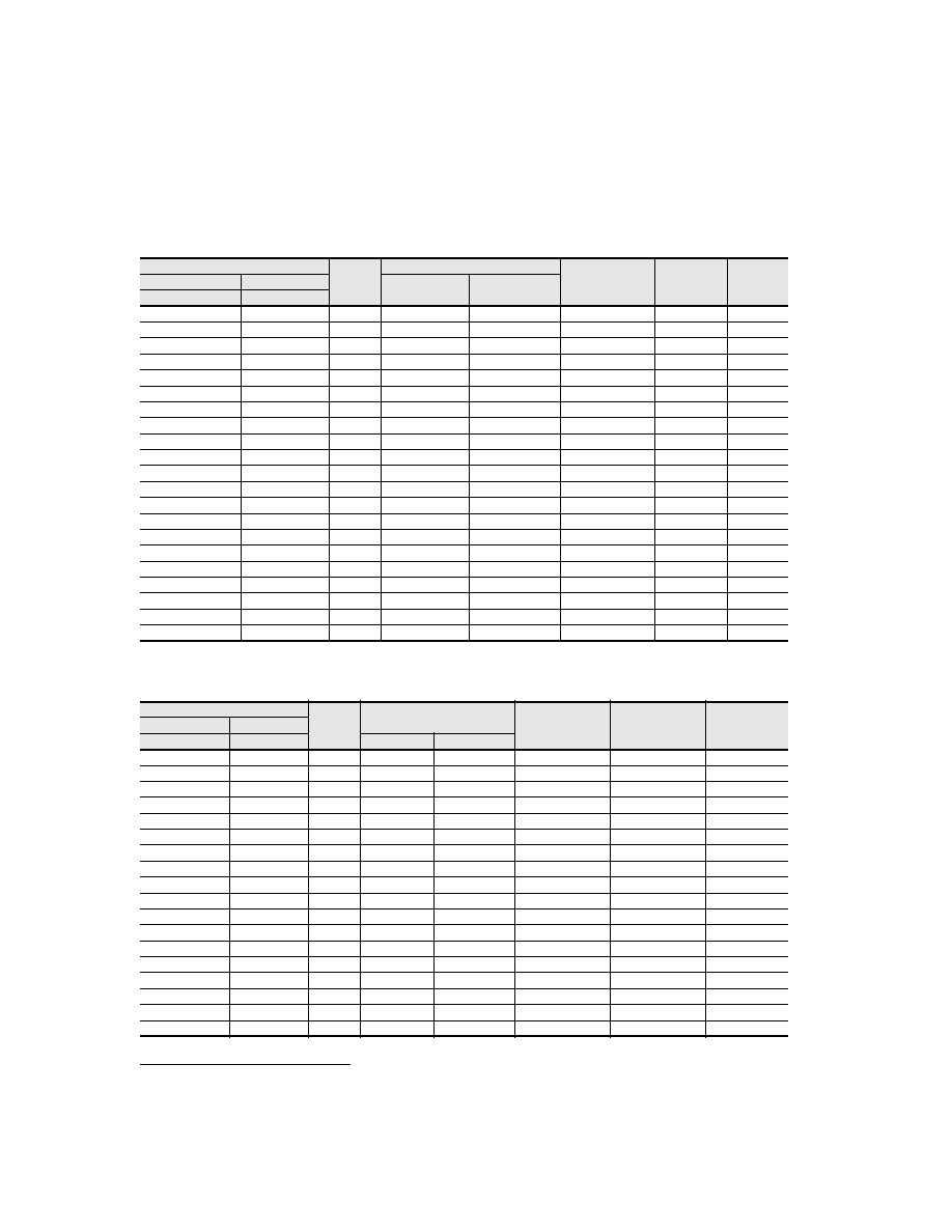
MG73Q/74Q Family Listing
E/A
# of
Pads
Usable Gate
Raw Gate
Column
Row
Product Name
Base Array
MG73Q
MG74Q
MG7XQ
B7XQ
B02
017x017
68
6,000
8,000
9,152
176
52
B04
027x027
108
17,000
23,000
25,800
300
86
B06
037x037
148
33,000
47,000
51,240
420
122
B08
047x047
188
55,000
78,000
85,952
544
158
B10
057x057
228
80,000
115,000
129,592
668
194
B12
067x067
268
106,000
154,000
181,240
788
230
B14
077x077
308
135,000
201,000
242,592
912
266
B16
087x087
348
165,000
239,000
311,664
1,032
302
B18
097x097
388
198,000
291,000
388,416
1,156
336
B20
107x107
428
233,000
333,000
476,160
1,280
372
B22
117x117
468
268,000
388,000
571,200
1,400
408
B24
127x127
508
304,000
439,000
676,656
1,524
444
B26
137x137
548
348,000
506,000
791,040
1,648
480
B28
147x147
588
383,000
547,000
912,288
1,768
516
B30
157x157
628
417,000
605,000
1,044,384
1,892
552
B32
167x167
668
448,000
636,000
1,179,032
2,012
586
B34
177x177
708
478,000
690,000
1,328,592
2,136
622
B36
187x187
748
520,000
743,000
1,487,080
2,260
658
B38
197x197
788
561,000
792,000
1,651,720
2,380
694
B40
207x207
828
603,000
840,000
1,827,920
2,504
730
B42
217x217
868
643,000
904,000
2,009,984
2,624
766
MSM98Q/99Q Family Listing
E/A
# of
PAD
Usable Gate
Raw Gate
Column
Row
Product Name
Base Array
MSM9xQ
B9xQ
M98Q
M99Q
B06
036x036
144
138,400
B10
044x044
176
128,000
184,000
214,000
856
250
B11
048x048
192
149,000
216,000
257,560
940
274
B12
050x050
200
159,000
229,000
280,280
980
286
B13
052x052
208
170,000
244,000
305,152
1,024
298
B14
056x056
224
192,000
278,000
356,776
1,108
322
B15
060x060
240
213,000
308,000
411,048
1,188
346
B16
064x064
256
240,000
343,000
470,640
1,272
370
B17
068x068
272
268,000
381,000
536,976
1,356
396
B18
072x072
288
296,000
417,000
604,800
1,440
420
B19
076x076
304
324,000
460,000
676,656
1,524
444
B20
080x080
320
353,000
504,000
752,544
1,608
468
B21
084x084
336
382,000
539,000
830,496
1,688
492
B22
088x088
352
402,000
576,000
914,352
1,772
516
B23
092x092
368
430,000
611,000
1,002,240
1,856
540
B24
096x096
384
461,000
658,000
1,098,040
1,940
566
B25
100x100
400
477,000
680,000
1,194,160
2,024
590
B26
104x104
416
503,000
710,000
1,291,856
2,104
614

≠≠≠≠≠≠≠≠≠≠≠≠≠≠≠≠≠≠≠≠≠≠≠≠≠≠≠≠≠≠≠≠≠≠≠≠≠≠≠≠≠≠≠≠≠≠≠≠≠≠≠≠≠≠≠≠≠≠≠≠≠≠≠≠≠
I
MG73Q/74Q and MSM98Q/99Q
I
3
Oki Semiconductor
ARRAY ARCHITECTURE
The primary components of a 0.35µm MG73Q/74Q and MSM98Q/99Q circuit include:
∑ I/O base cells: 60-µm staggered I/O pitch (MG73Q/74Q) or 100-µm In-Line I/O pitch
(MSM98Q/99Q)
∑ Configurable I/O pads for V
DD
, V
SS
, or I/O (optimized 3-V I/O and 3-V I/O that is 5-V tolerant)
∑ V
DD
and V
SS
pads dedicated to wafer probing
∑ Separate power bus for output buffers
∑ Separate power bus for internal core logic and input buffers
∑ Core base cells containing N-channel and P-channel pairs, arranged in column of gates
∑ Isolated gate structure for reduced input capacitance and increased routing flexibility
Each array has 24 dedicated corner pads for power and ground use during wafer probing, with four pads
per corner. The arrays also have separate power rings for the internal core functions (V
DDC
and V
SSC
)
and output drive transistors (V
DDO
and V
SSO
).
Figure 7. MSM98Q000 Array Architecture
Core base cell
with 4 transistors
Separate power bus (V
DDO
, V
SSO
)
over I/O cell for output buffers(2nd
metal/3rd metal)
V
DD
, V
SS
pads (4) in each
corner for
wafer probing only
Configurable I/O pads
for V
DD
, V
SS
, or I/O
Separate power bus (V
DDC
, V
SSC
) for
internal core logic (2nd metal/3rd metal
I/O base cells
Up to 3- or 4-layer metal
interconnection in core
area