
Ether-PON ONT Transceiver Preliminary
Specifications
Document NO: QPS-0201-046
Rev. DRAFT1.0
1/9
Preliminary
Ether-PON ONT Transceiver
Specifications
Part Number : OAT1233S-ONU-V4-A
Modification History
Rev.
Date
Originator
Comment
Rev. Draft0.2
Nov.27, 2001
H. Okada
Table 1.2 PN Modification
Rev. Draft0.3
Dec.28, 2001
T.Tanaka
Addition of Figure1.1, Table1.4, Figure4.1 and 4.2
Rev. Draft0.4
May.7, 2002
T.Tanaka
Change Specification and Characteristics.
Rev. Draft0.5
May.9, 2002
T.Tanaka
Change Table3.1
Rev. Draft0.6
May.27, 2002
T.Tanaka
Addition of Attenuation range and Path penlty
Rev. Draft0.7
May.29, 2002
T.Tanaka
Addition of note sentence (Figure4.1)
Change the Bet Error Ratio of Table1.2
Rev. Draft0.8
July.15, 2002
T.Tanaka
Change specification
Rev. Draft0.9
Sep.17, 2002
T.Tanaka
Change specification
Rev. Draft1.0
Dec.10, 2002
T.Tanaka
Change specification
1.Specifications
Table 1.1 Specifications
Parameter
Unit
Specifications
Bit rate
Gbit/s
1.250
Transmission mode
-
Tx: burst, Rx: continuous
Transfer code
-
NRZ
Bi-directional transmission
-
1-fibre WDM
Transmission distance
km
less than 7 @ FP-LD
Laser diode
-
1.31um FP
Photo detector
-
PIN-PD
Attenuation range
dB
16 � 20(*)
Path penalty
dB
1
Operating temperature range
�C
0 ~ 70
Operating humidity
%
5 ~ 95
Fiber/Connector type
-
Single mode fiber (10/125nm) / PC polished SC connector
Power supply voltage
V
+3.3 +/-5%
Power consumption
W
2.0W (typ.) , 3.0W(Max.)
Dimension
mm
40 � 60 � 8.5
*: Attenuation range matches OKI's OLT module specification.
Document Number QPS-0201-046
DATE: Nov. 16, 2001
Author H.Ishizaki
Project Manager K. YUSA

Ether-PON ONT Transceiver Preliminary
Specifications
Document NO: QPS-0201-046
Rev. DRAFT1.0
2/9
Preliminary
Table 1.2 Optical Characteristics (over operating temperature and lifetime)
Parameter
Unit
Specifications
Part number
OAT1233S-ONU-V4-A
Operating wavelength
nm
Tx
:1270
- 1360/Rx:1480 -1580
Mask of the transmitter eye diagram
Figure1.1
Maximum reflectance of equipment, measured at
transmitter wavelength
dB
-6
Mean launched power range
dBm
-1.0 ~ +3.0
Minimum extinction ratio
dB
9
Tolerance to the transmitter incident light
power
dB
more than -15
Launched optical power
w/o input to the transmitter
dBm
less than -43
Maximum spectral width
nm
2.5 (rms) @FP-LD
Side mode suppression ratio (@DFB-LD)
dB
-
Jitter transfer
dB
TBD
Jitter generation in 1.3kHz bandwidth
UIpp
TBD
Maximum reflectance of equipment,
measured at receiver wavelength
dB
less than -20
Bit error ratio
-
less than 10
-12
Minimum sensitivity
dBm
-22.0
Minimum overload
dBm
-2.0
Consecutive identical digit immunity
bit
more than 72
Jitter tolerance
-
TBD
Tolerance to the reflected optical power
dB
less than 10
Table 1.3 Absolute maximum ratings
Parameter
Symbol
Conditions
Ratings
Unit
Power supply voltage
Vcc
0 to +4.6
V
Input voltage
Vi
0 to Vcc
V
Maximum output current
Io
Ta = 25�C
30
mA
Storage temperature
Tstg
-40 to +85
�C
Soldering temperature/time
Ta = 25�C
250/10
�C/sec
Maximum tension of fiber
500
g
Minimum bending radius
30
mm
Ether-PON ONT Transceiver Preliminary
Specifications
Document NO: QPS-0201-046
Rev. DRAFT1.0
3/9
Preliminary
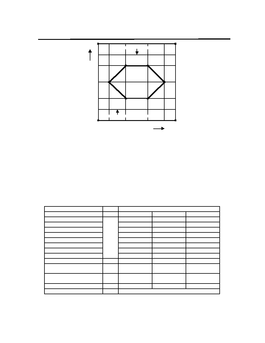
Figure1.1 Eye mask pattern for OAT1233-ONU
Table1.4 DC Characteristic
Parameter
Unit
OAT1233-ONU-Vxx-A/B
MIN
TYP
MAX
PECL input high voltage
VCC-1.17
-
VCC-0.88
PECL input low voltage
VCC-1.81
-
VCC-1.47
PECL output high voltage
VCC-1.02
-
VCC-0.88
PECL output low voltage
VCC-1.81
-
VCC-1.62
LVTTL input high voltage
2.0
-
VCC+0.3
LVTTL input low voltage
-0.3
-
0.8
LVTTL output high voltage
2.4
-
Vcc
LVTTL output low voltage
V
GND
-
0.4
Clock input duty
%
40
50
60
Data output rise/fall time ( 20
- 80 % )
ns
2.5
Clock/Data input setup &
hold time
-
Figure4.1
Pre-bias input timing
-
Figure4.2
Required preamble pattern
-
1010101010101010
1.2
Amplitude
UI
0.20
0
0.5
1
0.22
0
-0.20
0.80
0.375
0.625
0.78
1
Mean level of logical 1
Mean level of logical 0

Ether-PON ONT Transceiver Preliminary
Specifications
Document NO: QPS-0201-046
Rev. DRAFT1.0
4/9
Preliminary
2. Block diagram
Fig. 2.1 Block diagram
PD
LD
PD
LD Driver
Temp.
Compensation
D-FF
TF
Alarm
1310nm
OPT I/O
1490 or 1550nm/
1310nm
WDM
CLK IN
DATA IN
PRE-BIAS IN
SHUT IN
Retiming
Regenerating
Reshaping
Pre-amp
1490 or 1550nm
DATA OUT
CLK OUT
LOS
CLKSEL

Ether-PON ONT Transceiver Preliminary
Specifications
Document NO: QPS-0201-046
Rev. DRAFT1.0
5/9
Preliminary
3. Pin description
Table 3.1 Pin descriptions
No.
I/O
Symbol
Level
Logic Functionality
01
SVCC
+3.3V
02
GND
Ground
03
I
SHUT
LV-TTL
P
Optical output shut down
04
O
TF
LV-TTL
P
Transmitter Failure alarm
05
I
CLKSEL
VCC or GND
Tx clock select(active GND), used if data is clocked into MOD
06
I
BIASP
LV-PECL
P
Pre-bias input (pos.)
07
I
BIASN
LV-PECL
N
Pre-bias input (neg.)
08
GND
Ground
09
I
SDATAP
LV-PECL
P
Data input (pos.)
10
I
SDATAN
LV-PECL
N
Data input (neg.)
11
I
ICLKP
LV-PECL
P
Clock input (pos.)
12
I
ICLKN
LV-PECL
N
Clock input (neg.)
13
GND
Ground
14
O
LOS
LV-TTL
P
Loss of incoming signal alarm
15
GND
Ground
16
O
RDATAN
LV-PECL
N
Data output (neg.)
17
O
RDATAP
LV-PECL
P
Data output (pos.)
18
GND
Ground
19
O
RCLKN
LV-PECL
N
Clock output (neg.)
20
O
RCLKP
LV-PECL
P
Clock output (pos.)
21
GND
Ground
22
GND
Ground
23
RVCC1
+3.3V
24
RVCC2
+3.3V