
G.983.3 Option2 FSAN OLT Transceiver
OAT1523S-OLT2-V2-B-10
Oki Electric Industry Co., Ltd.
1/6
April/2002
Document NO: QPS-0202-002
Rev. DRAFT 0.2
G.983.3 Option2 FSAN OLT
Transceiver Specifications
Part Number : OAT1523S-OLT2-V2-B-10
ITU-T G.983.3 Option2 Class B acceptable
Modification History
Rev.
Date
Originator
Comment
DRAFT0.1
Apr. 2, 2002
H. OKADA
DRAFT0.2
Apr. 11, 2002
H. OKADA
Modification of Block diagram, Pin description(No.9)
1. Specifications
Table 1.1 Specifications
Parameter
Unit
Specifications
Bit rate
Mbit/s
Tx:622.08 , Rx:155.52
Transmission mode
-
Tx: continuous, Rx: burst
Transfer code
-
NRZ
Bi-directional transmission
-
1-fibre WDM
Transmission distance
km
20
Laser diode
-
1.49um DFB-LD
photo detector
-
PIN-PD
Operating temperature range
�
C
0 ~ 70
Operating humidity
%
5 ~ 90
Fiber/Connector type
-
Single mode fiber (10/125nm) / PC polished SC connector
Power supply voltage
V
+3.3 +/-5%
Power consumption
W
1.2 (typ.) , 1.4(max.)
Dimension
mm
40
�
60
�
8.5
Document Number QPS-0202-002
Revision DRAFT 0.2
DATE: April. 11, 2002
Author H. OKADA
Project Manager K. YUSA

G.983.3 Option2 FSAN OLT Transceiver
OAT1523S-OLT2-V2-B-10
Oki Electric Industry Co., Ltd.
2/6
April/2002
Document NO: QPS-0202-002
Rev. DRAFT 0.2
Table 1.2 Optical Characteristics (over operating temperature and lifetime)
Parameter
Unit
Specifications
Operating wavelength
nm
Tx:1480 - 1500 / Rx:1260 - 1360
Mask of the transmitter eye diagram
ITU-T G.983 Downstream
Maximum reflectance of equipment, measured at
transmitter wavelength
dB
-
Mean launched power range
dBm
SOL +1.5 ~ +4.0
EOL +1.0 ~ +4.0
Minimum extinction ratio
dB
10
Tolerance to the transmitter incident light
power
dB
more than -15
Launched optical power
w/o input to the transmitter
dBm
-
Maximum spectral width
nm
1 (@-20dB)
Side mode suppression ratio
dB
more than 30
Jitter transfer
-
Jitter generation in 1.3kHz bandwidth
UIpp
-
Maximum reflectance of equipment,
measured at receiver wavelength
dB
less than -20
Bit error ratio
-
less than 10
-10
Minimum sensitivity
dBm
SOL -33.5
EOL -33.0
Minimum overload
dBm
SOL -7.5
EOL -8.0
Consecutive identical digit immunity
-
more than 72
Jitter tolerance
-
-
Tolerance to the reflected optical power
dB
less than 10
Table 1.3 Absolute maximum ratings
Parameter
Symbol
Conditions
Ratings
Unit
Power supply voltage
Vcc
0 to +4.6
V
Input voltage
Vi
0 to Vcc
V
Maximum output current
Io
Ta = 25
�
C
30
mA
Storage temperature
Tstg
-40 to +85
�
C
Soldering temperature/time
Ta = 25
�
C
250/10
�
C/sec
Maximum tension of fiber
500
g
Minimum bending radius
30
mm

G.983.3 Option2 FSAN OLT Transceiver
OAT1523S-OLT2-V2-B-10
Oki Electric Industry Co., Ltd.
3/6
April/2002
Document NO: QPS-0202-002
Rev. DRAFT 0.2
2. Block diagram
Fig. 2.1 Block diagram
PD
LD
PD
LD Driver
Alarm
TF
1310nm
OPT I/O
1310nm/1490nm
WDM
CLK IN
DATA IN
SHUT IN
CDR
ATC
Pre-amp
1490nm
DATA OUT
CLK OUT
SYNC. LOSS
TD
CDR RESET IN
ATC RESET IN
POC IN
Temp.
compensation

G.983.3 Option2 FSAN OLT Transceiver
OAT1523S-OLT2-V2-B-10
Oki Electric Industry Co., Ltd.
4/6
April/2002
Document NO: QPS-0202-002
Rev. DRAFT 0.2
3. Pin description
Table 3.1 Pin descriptions
No. I/O Symbol
Level Logic Functionality
01
SVCC
Transmitter power supply (+3.3V)
02
GND
Ground
03
I SDATAP
LVPECL
Data input (pos) :622.08Mbps
04
I SDATAN
LVPECL
P
Data input (neg) :622.08Mbps
05
I BCLKP
LVPECL
CDR Clock input (pos) :155.52Mbps
06
I BCLKN
LVPECL
P
CDR Clock input (neg) :155.52Mbps
07
GND
Ground
08
I SHUT
LVTTL
P
Optical output shut down
09
NC
Not user connection
10 O TD
LVTTL
P
Transmitter Degraded alarm
11 O TF
LVTTL
P
Transmitter Failure alarm
12
GND
Ground
13
GND
Ground
14 O ALM
LVTTL
P
Sync. out alarm
15
GND
Ground
16
I POC
LVTTL
N Power on clear
17
I BRSP
LVPECL
CDR reset (pos)
18
I BRSN
LVPECL
N
CDR reset (neg)
19
GND
Ground
20 O RCLKP
LVPECL
Clock output (pos)
21 O RCLKN
LVPECL
P
Clock output (neg)
22
GND
Ground
23 O RDATAP
LVPECL
Data output (pos)
24 O RDATAN
LVPECL
P
Data output (neg)
25
GND
Ground
26
BVCC
Power supply for CDR (+3.3V)
27
GND
Ground
28
GND
Ground
29
I RSN
LVPECL
ATC reset (neg)
30
I RSP
LVPECL
N
ATC reset (pos)
31
GND
Ground
32
RVCC
Power supply for ATC (+3.3V)
G.983.3 Option2 FSAN OLT Transceiver
OAT1523S-OLT2-V2-B-10
Oki Electric Industry Co., Ltd.
5/6
April/2002
Document NO: QPS-0202-002
Rev. DRAFT 0.2
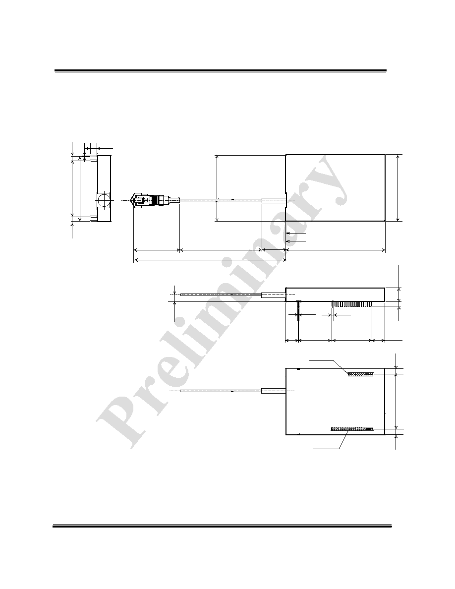
4. Outline
(1)
(12)
(32)
(13)
30.32�0.3
12 -
0
.45
19x1.27
=24.13�0.3
7.775
8.5MAX
(3.39)
13x2.54 = 33.02�0.3
(3.39)
(7.8)
20 -
0
.45
40�1
60�1
(TOP View)
0.8
1.27
(3.1)
(4.9)
(6.6)
(0.4)
(3.29)
3.29
(3.6)
33.0 � 0.3
39.6 � 0.3
(38)
1060
+100
-100
(10)
27.9
(4.125)
12.1
Fig 4.1 Package Outline

G.983.3 Option2 FSAN OLT Transceiver
OAT1523S-OLT2-V2-B-10
Oki Electric Industry Co., Ltd.
6/6
April/2002
Document NO: QPS-0202-002
Rev. DRAFT 0.2
5. Precautions for handling
The circuits of these modules operate at very small signal. In order to avoid the degradation of the optical
sensitivity due to external noise, the bottom pattern of these modules on the PCB should be ground pattern
with low impedance.
Do not mount/pattern device/circuits which generate high frequency noise close to the module.
In order to operate the module stable against the power noise, install the power supply noise reduction circuits.
The impedance between the power and ground pattern of the power circuit should be as low as possible. The
elements around the module should be mounted close to the pins of the module.
If an optical power exceeding the absolute maximum ratings is fed to the module, the optical receiver may be
damaged. Set the optical input power appropriately when in use of these modules.
6. Qualification and Reliability
To help ensure high product reliability and customer satisfaction, OKI is committed to an intensive quality
program that starts in the design phase and proceeds through the manufacturing process.
Optical transceiver modules are qualified to OKI internal standards using MIL-STD-883 test methods and
procedures and using sample techniques consistent with Telcordia requirements.
This qualification program fully meets the intent of Telcordia reliability practices GR-468-CORE.
7. Laser Safety
All version of transceiver are Class 1 Laser products FDA complies with 21 CFR 1040.10 and 1040.11
requirements.
Also, all versions are Class 1 Laser products pre IEC 825-1.