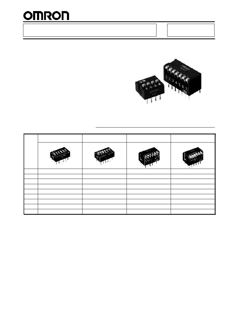
ChipFind - документация

Электронный компонент: A6ER-8101

Скачать:  PDF   ZIP

Document Outline

R
DIP Switch
A6E/A6ER
DIP Switch
H
The sealed bottom prevents flux
penetration
H
A variety of models including models
with short or long levers are available
Ordering Information
No. of
poles
Flat actuated
Raised actuator
Side actuated (short-lever)
Side actuated (long-lever)
DIP terminal
DIP terminal
DIP terminal
DIP terminal
2
A6E-2101
A6E-2104
A6ER-2101
A6ER-2104
3
A6E-3101
A6E-3104
A6ER-3101
A6ER-3104
4
A6E-4101
A6E-4104
A6ER-4101
A6ER-4104
5
A6E-5101
A6E-5104
A6ER-5101
A6ER-5104
6
A6E-6101
A6E-6104
A6ER-6101
A6ER-6104
7
A6E-7101
A6E-7104
A6ER-7101
A6ER-7104
8
A6E-8101
A6E-8104
A6ER-8101
A6ER-8104
9
A6E-9101
A6E-9104
A6ER-9101
A6ER-9104
10
A6E-0101
A6E-0104
A6ER-0101
A6ER-0104
Important note: Switches cannot be water-washed.
A6E/A6ER
A6E/A6ER
200
Specifications
J
CHARACTERISTICS
Switching capacity
25 mA at 24 VDC
Insulation resistance
100 MW min. (at 250 VDC)
Contact resistance
200 mW max. (initial value)
Dielectric strength
500 VAC for 1 min between terminals of same polarity, and between terminals of
different polarity
Vibration resistance
Malfunction: 10 to 55 Hz, 1.5-mm double amplitude
Shock resistance
Malfunction: 300 m/s
2
min. (approx. 30G min.)
Life expectancy
Mechanical
1,000 operations min.
Life expectancy
Electrical
1,000 operations min.
Ambient temperature
Operating
--20C to 70C (with no icing)
Ambient humidity
Operating
35% to 90%
Operating force
0.29 N min. (30 gf)
Dimensions
Unit: mm (inch)
Note: Unless otherwise specified, a tolerance of 0.4 mm applies to all dimensions.
J
FLAT ACTUATED WITH
DIP TERMINAL
A6E-j101
Flat Actuated
Raised Actuator
J
RAISED ACTUATOR
WITH DIP TERMINAL
A6E-j104
PCB Dimensions
(Top View)
1.00.05 dia.
No. of poles
Part number
A
2
A6E-2101
A6E-2104
6.64
3
A6E-3101
A6E-3104
9.18
4
A6E-4101
A6E-4104
11.72
5
A6E-5101
A6E-5104
14.26
6
A6E-6101
A6E-6104
16.80
7
A6E-7101
A6E-7104
19.34
8
A6E-8101
A6E-8104
21.88
9
A6E-9101
A6E-9104
24.42
10
A6E-0101
A6E-0104
26.96
A6E/A6ER
A6E/A6ER
201
J
DIP TERMINAL
SIDE ACTUATED
(SHORT-LEVER)
A6ER-j101
Side Actuated
(short-lever)
Side Actuated
(long-lever)
J
SIDE ACTUATED
(LONG-LEVER)
A6ER-j104
PCB Dimensions
(Top View)
1.00.05 dia.
No. of poles
Part number
A
2
A6ER-2101
A6ER-2104
6.64
3
A6ER-3101
A6ER-3104
9.18
4
A6ER-4101
A6ER-4104
11.72
5
A6ER-5101
A6ER-5104
14.26
6
A6ER-6101
A6ER-6104
16.80
7
A6ER-7101
A6ER-7104
19.34
8
A6ER-8101
A6ER-8104
21.88
9
A6ER-9101
A6ER-9104
24.42
10
A6ER-0101
A6ER-0104
26.96
A6E/A6ER
A6E/A6ER
202
Installation
J
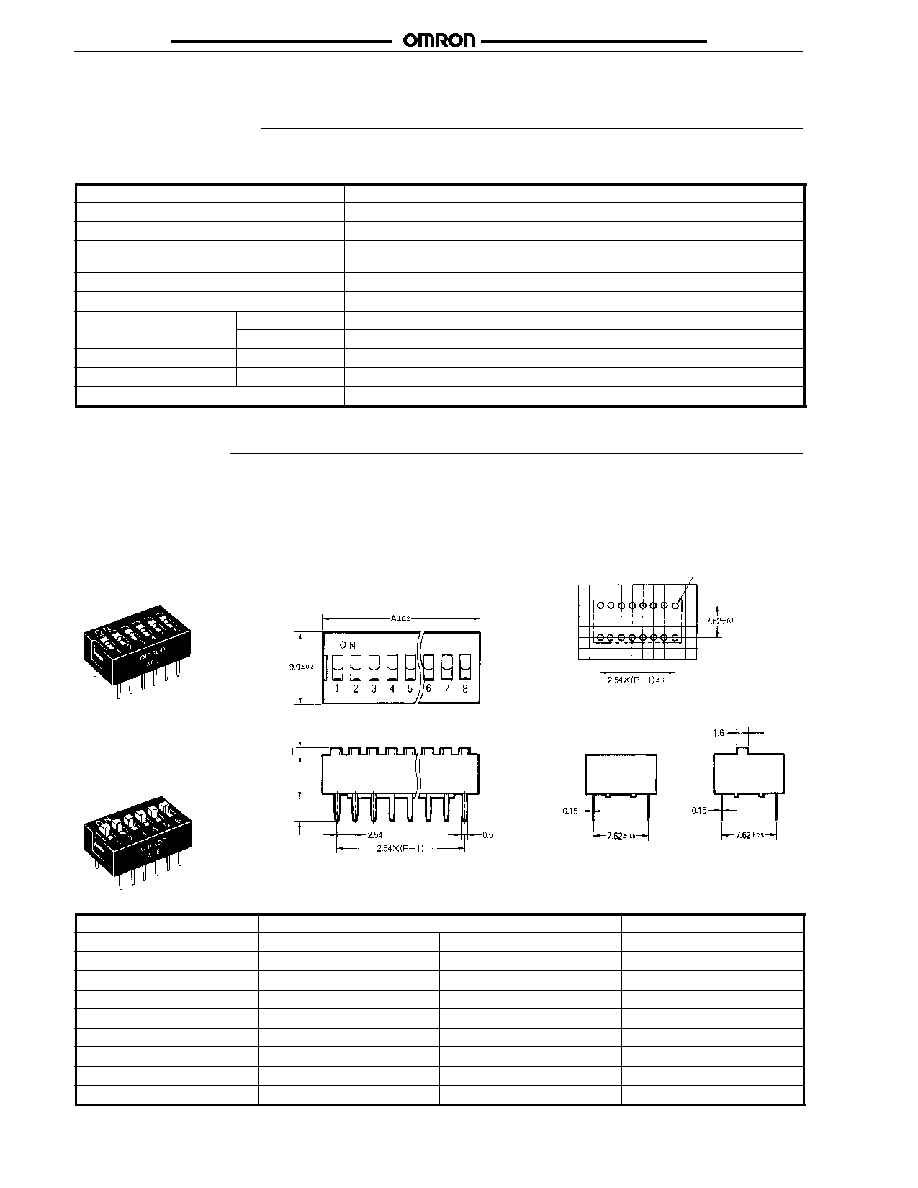
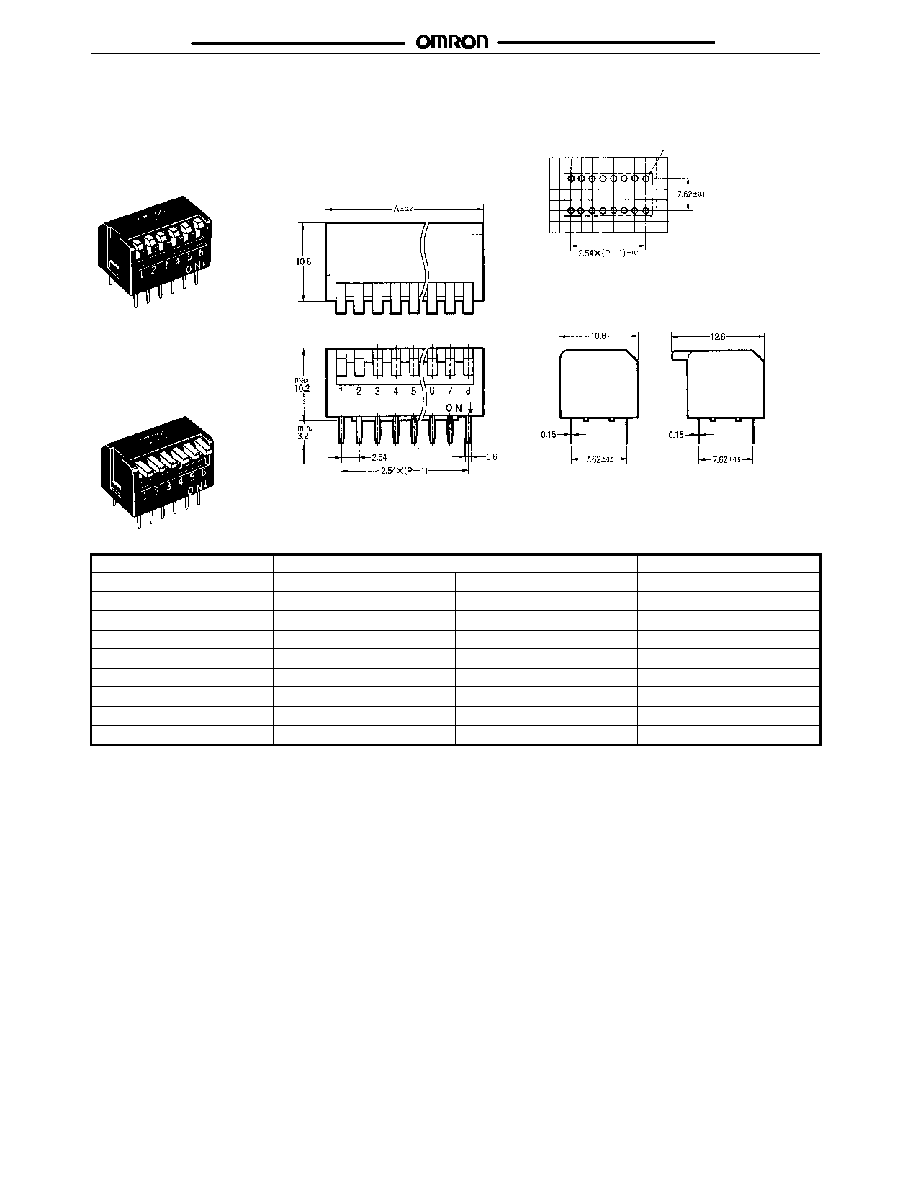
INTERNAL CONNECTIONS (TOP VIEW)
Precautions
J
CIRCUIT DESIGN
Use the DIP Switch within the rated voltage and current ranges,
otherwise the DIP Switch may have a shortened life expectancy,
radiate heat, or burn out.
J
MOUNTING
Do not operate the DIP Switch while mounting, soldering, or wash-
ing the DIP Switch, otherwise the DIP Switch may deform due the
heat of the solder, the DIP Switch may malfunction due to the pe-
netration of the washing agent, or the machine incorporating the
DIP Switch may operate or be set incorrectly.
An automatic insertion machine incorporating a body stopper is
available for mounting the DIP Switch. When usingan automatic in-
sertion machine incorporating a half-lead stopper to mount the DIP
Switch, make sure that the automatic insertion machine will not de-
form the terminals of the DIP Switch, otherwise the improper inser-
tion of the DIP Switch may result.
J
SOLDERING
Observe the following conditions when soldering the DIP Switch.
Automatic Soldering Bath
Soldering temperature: 260C max.
Soldering time:
5 s max. for a 1.6-mm thick,
single-side PCB
Reflow Soldering
Soldering time
Soldering
temperature
(C)
2 minutes
max.
20 seconds
max.
Manual Soldering
Soldering temperature: 350C at the tip of the soldering iron.
Soldering time:
3 s max. for a 1.6-mm thick,
single-side PCB
Set the pins of the DIP Switch to OFF before soldering the DIP
Switch.
Before soldering the DIP Switch on a PCB, make sure that there is
no unnecessary space between the DIP Switch and PCB.
Before soldering the DIP Switch on a multilayer PCB, make sure
that the DIP Switch will not bedeformed by the solderingheat onthe
pattern or land of the multilayer PCB.
Do not solder the DIP Switch more thantwice includingrectification
soldering. An interval of five minutes is required between the first
and second solderings.
Make sure that there is no flux rise on the surface of the PCB.
PCB surface
Flux
J
WASHING
The A6E/A6ER DIP Switches are not washable.
J
HANDLING
Donot apply excessiveoperatingforceto theDIP Switch, otherwise
the DIP Switch may be damaged or deformed, thus causing the
switch mechanism to malfunction as a result. Apply an operating
force not exceeding 200% of the maximum rated operating force to
the DIP Switch.
Set the DIP Switch incorporating slide pins with a tiny, rounded ob-
ject, such as the tip of a ball-point pen or small screwdriver. Do not
set the DIP Switch using tweezers or any other sharp object, which
may damage the DIP Switch. Do not set the DIP Switch using the
point of a mechanical pencil, otherwise lead powder or fragments
may fall into the DIP Switch and internal circuit board, causing the
DIPSwitchtomalfunctionand reducingthe dielectric strength of the
circuit board.
A6ER A6ER
Cat. No. GC SW6 04/01 Specifications subject to change without notice. Printed in U.S.A.
OMRON ELECTRONICS LLC
One East Commerce Drive
Schaumburg, IL 60173
NOTE: DIMENSIONS SHOWN ARE IN MILLIMETERS. To convert millimeters to inches divide by 25.4.
1-800-55-OMRON
OMRON CANADA, INC.
885 Milner Avenue
Scarborough, Ontario M1B 5V8
416-286-6465
R
OMRON ON--LINE
Global -- http://www.omron.com
USA -- http://www.omron.com/oei
Canada -- http://www.omron.com/oci