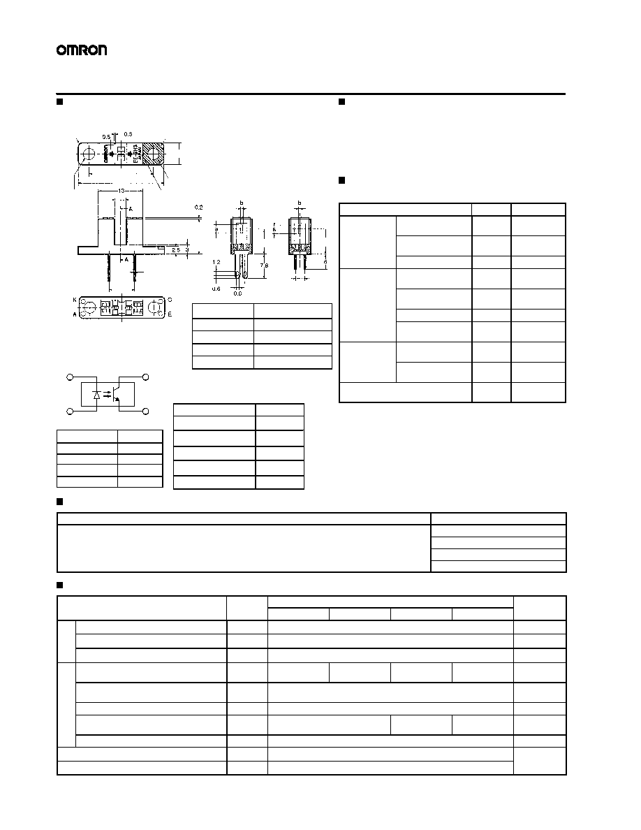
Terminal No.
Name
A
Anode
K
Cathode
C
Collector
E
Emitter
Dimensions
Tolerance
3 mm max.
±0.2
3 < mm 6
±0.24
6 < mm 10
±0.29
10 < mm 18
±0.35
18 < mm 30
±0.42
Internal Circuit
K
A
C
E
Unless otherwise specified, the
tolerances are as shown below.
Four, 0.25
Two, 3.2 dia.
holes
Two, C1.5
Four, R1
Matted
Center mark
Solder terminal
Cross section AA
PCB terminal
Cross section AA
Model
Aperture (a x b)
EE-SH3(-B)
2.1 x 0.5
EE-SH3-C(S)
2.1 x 1.0
EE-SH3-D(S)
2.1 x 0.2
EE-SH3-G(S)
0.5 x 2.1
19±0.15
25.4
3.4±0.2
2.54±0.2
7.2±0.2
7.2±0.2
7.6±0.3
6.2
10.2
Photomicrosensor
(Transmissive)
EE-SH3 Series
Dimensions
Note: All units are in millimeters unless otherwise indicated.
Features
∑
All models have 3.4 mm wide slot.
∑
Solder terminal models:
EE-SH3/-SH3-CS/-SH3-DS/-SH3-GS
∑
PCB terminal models:
EE-SH3-B/-SH3-C/-SH3-D/-SH3-G
Absolute Maximum Ratings
(Ta = 25∞C)
Item
Symbol
Rated value
Emitter
Forward current
I
F
50 mA
(see note 1)
Pulse forward
current
I
FP
1 A
(see note 2)
Reverse voltage
V
R
4 V
Detector
Collector--Emitter
voltage
V
CEO
30 V
Emitter--Collector
voltage
V
ECO
---
Collector current
I
C
20 mA
Collector
dissipation
P
C
100 mW
(see note 1)
Ambient
temperature
Operating
Topr
--25∞C to
85∞C
Storage
Tstg
--30∞C to
100∞C
Soldering temperature
Tsol
260∞C
(see note 3)
Note: 1. Refer to the temperature rating chart if the ambient
temperature exceeds 25∞C.
2. The pulse width is 10 µs maximum with a frequency
of 100 Hz.
3. Complete soldering within 10 seconds.
Ordering Information
Description
Part number
Photomicrosensor (Transmissive)
EE-SH3(-B)
o o c ose so ( a s ss e)
EE-SH3-C(S)
EE-SH3-D(S)
EE-SH3-G(S)
Electrical and Optical Characteristics (Ta = 25∞C)
Item
Symbol
Value
Condition
EE-SH3(-B)
EE-SH3-C(S)
EE-SH3-D(S)
EE-SH3-G(S)
r
Forward voltage
V
F
1.2 V typ., 1.5 V max.
I
F
= 30 mA
m
itter
Reverse current
I
R
0.01 µA typ., 10 µA max.
V
R
= 4 V
Emi
t
Peak emission wavelength
P
940 nm typ.
I
F
= 20 mA
Light current
I
L
0.5 to 14 mA
typ.
1 to 28 mA typ.
0.1 mA min.
0.5 to 14 mA
I
F
= 20 mA,
V
CE
= 10 V
c
tor
Dark current
I
D
2 nA typ., 200 nA max.
V
CE
= 10 V,
0 x
e
tec
t
Leakage current
I
LEAK
---
---
De
t
Collector--Emitter saturated voltage
V
CE
(sat)
0.1 V typ., 0.4 V max.
---
0.1 V typ.,
0.4 V max.
I
F
= 20 mA,
I
L
= 0.1 mA
Peak spectral sensitivity wavelength
P
850 nm typ.
V
CE
= 10 V
Rising time
tr
4 µs typ.
V
CC
= 5 V,
R
L
= 100
Falling time
tf
4 µs typ.
R
L
= 100 ,
I
L
= 5 mA

EE-SH3 Series
EE-SH3 Series
Engineering Data
Forward Current vs. Collector
Dissipation Temperature Rating
Forward Current vs. Forward
Voltage Characteristics (Typical)
Light Current vs. Forward Current
Characteristics (Typical)
Ambient temperature Ta (∞C)
Collector
dissipation
Pc
(
mW)
Forward voltage V
F
(V)
F
Forward
c
urrent
I
(
mA)
F
Forward
c
urrent
I
(
mA)
Forward current I
F
(mA)
Light
current
I
(
mA)
L
Light Current vs. Collector--Emitter
Voltage Characteristics (EE-SH3(-B))
Relative Light Current vs. Ambi-
ent Temperature Characteristics
(Typical)
Dark Current vs. Ambient
Temperature Characteristics
(Typical)
Collector--Emitter voltage V
CE
(V)
Light
c
urrent
I
(
mA)
L
Ambient temperature Ta (∞C)
Ambient temperature Ta (∞C)
Response Time vs. Load Resis-
tance Characteristics (Typical)
Sensing Position Characteristics
(EE-SH3-D(S))
Load resistance R
L
(k)
Distance d (mm)
Sensing Position Characteristics
(EE-SH3(-B))
Distance d (mm)
Sensing Position Characteristics
(EE-SH3-G(S))
Distance d (mm)
Sensing Position Characteristics
(EE-SH3-C(S))
Distance d (mm)
Ta = --30∞C
Ta = 25∞C
Ta = 70∞C
I
F
= 20 mA
V
CE
= 5 V
V
CE
= 10 V
0 x
I
F
= 20 mA
V
CE
= 10 V
Ta = 25∞C
Vcc = 5 V
Ta = 25∞C
Input
Output
Input
Output
90 %
10 %
Ta = 25∞C
V
CE
= 10 V
I
F
= 50 mA
I
F
= 40 mA
I
F
= 30 mA
I
F
= 20 mA
I
F
= 10 mA
Ta = 25∞C
I
F
= 20 mA
V
CE
= 10 V
Ta = 25∞C
Center of optical axis
Center of optical axis
I
F
= 20 mA
V
CE
= 10 V
Ta = 25∞C
Center of optical axis
I
F
= 20 mA
V
CE
= 10 V
Ta = 25∞C
Center of optical axis
Relative
light
current
I
(
%)
L
Dark
current
I
(
nA)
D
Response
time
tr
,
tf
(
s
)
µ
Relative
light
current
I
(
%)
L
Relative
light
current
I
(
%)
L
Relative
light
current
I
(
%)
L
Relative
light
current
I
(
%)
L
Response Time Measurement
Circuit
I
F
Pc
d
0
--
+

Cat. No.
GC NAPMS≠1
02/03 Specifications subject to change without notice. Printed in U.S.A.
OMRON ELECTRONICS LLC
One East Commerce Drive
Schaumburg, IL 60173
NOTE: DIMENSIONS SHOWN ARE IN MILLIMETERS. To convert millimeters to inches divide by 25.4.
847≠882≠2288
OMRON CANADA, INC.
885 Milner Avenue
416-286-6465
R
OMRON ON≠LINE
Global ≠ http://www.omron.com
USA ≠ http://www.omron.com/oei
Canada ≠ http://www.omron.com/oci
Toronto, Ontario M1B 5V8