
1
G3VM-353A/B/D/E
MOS FET Relay
MOS FET Relay with N.C. (Normally
Closed) Contacts for Switching Analog
Signals
s
SPST-NC contact form.
s
Switches minute analog signals.
s
Switches AC and DC.
s
Low ON-resistance.
s
UL/CSA approval pending.
s
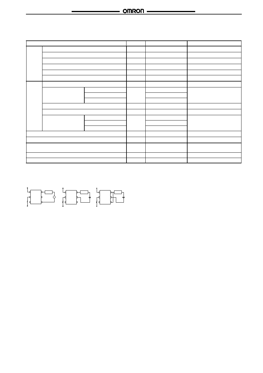
Appearance
Ordering Information
Application Examples
∑ Electronic automatic exchange systems
∑ Datacoms and modems
∑ Measuring systems
∑ Security systems
∑ FA
R
OMRON logo
Model name
LOT No.
Note: "G3VM" is not printed on the actual product.
Contact form
Terminals
Load voltage (peak
value)
Model
Number per stick
Taping quantity
SPST-NC
PCB terminals
350 VAC
G3VM-353A
100
---
G3VM-353B
50
Surface-mounting
terminals
G3VM-353D
100
G3VM-353E
50
G3VM-353D(TR)
---
1,500
G3VM-353E(TR)

2
G3VM-353A/B/D/E
G3VM-353A/B/D/E
Specifications
s
G3VM-353A/D
Absolute Maximum Ratings (Ta = 25
∞
C)
Note
The dielectric strength between I/O terminals was measured with voltage applied to all of the input pins and all of the output pins.
Electrical Performance (Ta = 25
∞
C)
Note
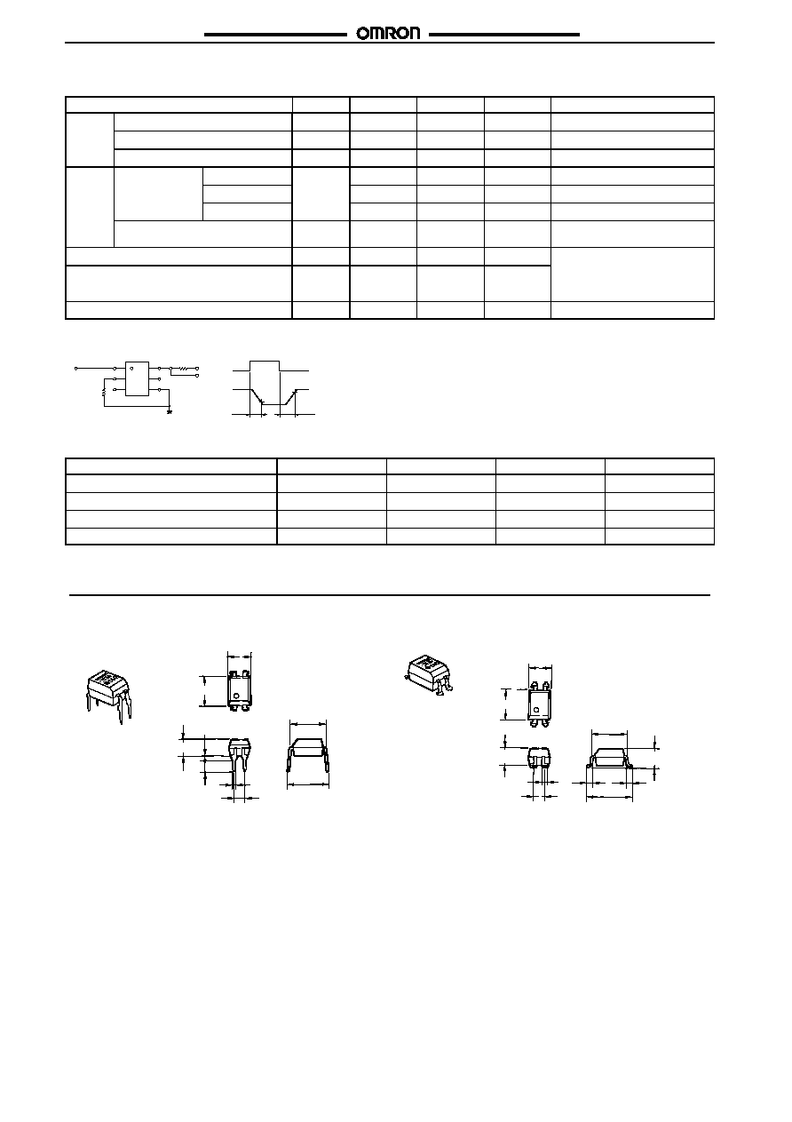
The operate and release time were measured in the way shown below.
Recommended Operating Conditions
Item
Symbol
Rating
Conditions
Input
LED forward current
I
F
50 mA
---
LED forward current reduction rate
I
F
/
∞
C
≠0.5 mA/
∞
C
Ta
25
∞
C
Repetitive peak LED forward current
I
FP
1 A
100-µs pulses, 100 pps
LED reverse voltage
V
R
5 V
---
Permissible loss
Pin
50 mW
---
Connection temperature
T
J
125
∞
C
---
Output
Output dielectric strength
V
OFF
350 V
AC peak value
Continuous load current
I
O
150 mA
---
Peak load current
I
peak
0.35 A
---
Output loss
P
out
506 mW
---
ON current reduction rate
I
ON
/
∞
C
≠1.5 mA/
∞
C
Ta
25
∞
C
Total permissible loss
P
T
556 mW
---
Dielectric strength between I/O terminals (See note.)
V
I≠O
2,500 Vrms
AC, 1 min
Insulation resistance
R
I≠O
5
◊
10
10
M
V
S
= 500 V, ambient operating humidity
60%
Storage temperature
Tstg
≠55 to
125
∞
C
---
Ambient operating temperature
Ta
≠40 to 85
∞
C
---
Item
Symbol
Minimum
Standard
Maximum
Conditions
Input
LED forward current
V
F
1.0 V
1.15 V
1.3 V
I
F
= 10 mA
Reverse current
I
R
---
---
10 µA
V
R
= 5 V
Capacity between terminals
C
T
---
30 pF
---
V = 0, f = 1 MHz
Output
Maximum resistance with output
ON
R
ON
---
15
25
I
ON
= 150 mA
Current leakage when the relay is
closed
I
LEAK
---
---
1 µA
V
OFF
= 350 V, I
F
= 5 mA
Turn-ON time
T
ON
---
0.1 ms
1 ms
R
L
= 200
(See note.)
V
DD
= 20 V,
I
F
= 5 mA
Turn-OFF time
T
OFF
---
1 ms
3 ms
Floating capacity between I/O terminals
C
I≠O
---
0.8 pF
---
V
S
= 0 V, f = 1 MHz
V
OUT
I
F
T
ON
T
OFF
10%
90%
I
F
1
2
4
3
R
L
V
DD
V
OUT
Item
Symbol
Minimum
Standard
Maximum
Operating voltage
V
DD
---
---
280 V
Forward current
I
F
5 mA
---
25 mA
Continuous load current
I
O
---
---
150 mA
Operating temperature
Ta
≠20
∞
C
---
65
∞
C
3
G3VM-353A/B/D/E
G3VM-353A/B/D/E
s
G3VM≠353B/E
Absolute Maximum Ratings (Ta = 25
∞
C)
Note
The dielectric strength between I/O terminals was measured with voltage applied to pins 1, 2, and 3 together, and to pins 4, 5, and
6 together.
Connection Circuit Diagram
Item
Symbol
Rating
Conditions
Input
LED forward current
I
F
50 mA
---
LED forward current reduction rate
I
F
/
∞
C
≠0.5 mA/
∞
C
Ta
25
∞
C
Repetitive peak LED forward current
I
FP
1 A
100-µs pulses, 100 pps
LED reverse voltage
V
R
5 V
---
Permissible loss
Pin
50 mW
---
Connection temperature
T
J
125
∞
C
---
Output
Output dielectric strength
V
OFF
350 V
AC peak value
Continuous load cur-
rent (See note.)
A connection
I
O
150 mA
---
B connection
150 mA
C connection
300 mA
Peak load current
I
peak
0.35 A
---
Output loss
P
out
506 mW
---
ON current reduction
rate
A connection
I
ON
/
∞
C
≠1.5 mA/
∞
C
Ta
25
∞
C
B connection
≠1.5 mA/
∞
C
C connection
≠3.0 mA/
∞
C
Total permissible loss
P
T
556 mW
---
Dielectric strength between I/O terminals (See note.)
V
I≠O
2,500 Vrms
AC, 1 min
Insulation resistance
R
I≠O
5
◊
10
10
M
V
S
= 500 V, ambient operating
humidity
60%
Storage temperature
Tstg
≠55 to 125
∞
C
---
Ambient operating temperature
Ta
≠40 to 85
∞
C
---
Load
or AC
DC
1
2
3
6
5
4
A connection
B connection
C connection
1
2
3
6
5
4
DC
Load
1
2
3
6
5
4
DC
Load
4
G3VM-353A/B/D/E
G3VM-353A/B/D/E
Electrical Performance (Ta = 25
∞
C)
Note
The operate and release time were measured in the way shown below.
Recommended Operating Conditions
Dimensions
Note
All units are in millimeters unless otherwise indicated.
Item
Symbol
Minimum
Standard
Maximum
Conditions
Input
LED forward current
V
F
1.0 V
1.15 V
1.3 V
I
F
= 10 mA
Reverse current
I
R
---
---
10 µA
V
R
= 5 V
Capacity between terminals
C
T
---
30 pF
---
V = 0, f = 1 MHz
Output
Maximum resis-
tance with out-
put ON
A connection
R
ON
---
15
25
I
ON
= 150 mA
B connection
---
8
14
I
ON
= 150 mA
C connection
---
4
7
I
ON
= 300 mA
Current leakage when the relay is
closed
I
LEAK
---
---
1 µA
V
OFF
= 350 V, I
F
= 5 mA
Operate time
T
ON
---
0.1 ms
1 ms
R
L
= 200
(See note.)
V
DD
= 20 V,
I
F
= 5 mA
Release time
T
OFF
---
1 ms
3 ms
Floating capacity between I/O terminals
C
I≠O
---
0.8 pF
---
V
S
= 0 V, f = 1 MHz
V
OUT
I
F
T
ON
T
OFF
10%
90%
V
OUT
6
5
4
1
I
F
2
3
V
DD
R
L
Item
Symbol
Minimum
Standard
Maximum
Operating voltage
V
DD
---
---
280 V
Forward current
I
F
5 mA
---
25 mA
Continuous load current
I
O
---
---
150 mA
Operating temperature
Ta
≠20
∞
C
---
65
∞
C
G3VM-353A
G3VM-353D
Note: "G3VM" is not printed on the actual product.
Weight: 0.26 g
Weight: 0.26 g
4.58
±
0.25
0.8
±
0.25
2.5 min.
2.54
±
0.25
7.62
±
0.25
7.85 to 8.80
0.5
±
0.1
6.4
±
0.25
3.65
0.15
-
0.25
4.58
±
0.25
1.0
min.
1.0 min.
2.54
±
0.25
7.62
±
0.25
10.0 max.
1.2
±
0.15
6.4
±
0.25
3.65
0.15
-
0.25
4.0
0.15
-
0.25
0.8
±
0.25
5
G3VM-353A/B/D/E
G3VM-353A/B/D/E
s
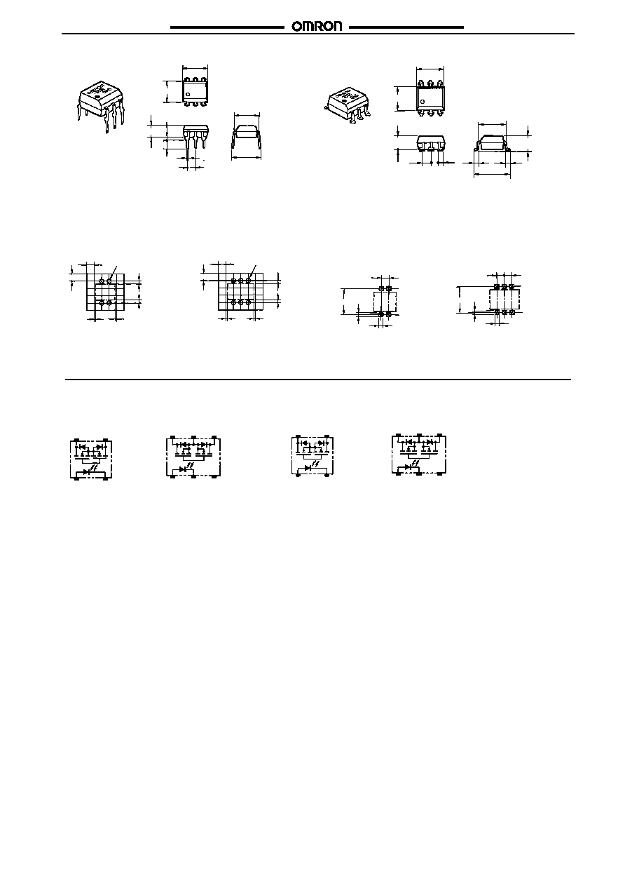
PCB Dimensions (Bottom View)
s
Actual Mounting Pad Dimensions
(Recommended Value, Top View)
Installation
s
Terminal Arrangement/Internal Connection (Top View)
G3VM-353B
G3VM-353E
Note: "G3VM" is not printed on the actual product.
Weight: 0.4 g
Weight: 0.4 g
7.12
±
0.25
7.62
±
0.25
0.8
±
0.25
2.5 min.
0.5
±
0.1
2.54
±
0.25
7.85 to 8.80
6.4
±
0.25
3.65
0.15
-
0.25
7.12
±
0.25
2.54
±
0.25
1.2
±
0.25
7.62
±
0.25
6.4
±
0.25
3.65
0.15
-
0.25
1.0
min.
1.0 min.
10.0 max.
4.0
0.15
-
0.25
G3VM-353A
G3VM-353B
2.54 Four, 0.8-dia. holes
0.1
0.1
0.56
0.56
2.54
2.54 Six, 0.8-dia. holes
0.1
0.1
0.56
0.56
2.54
G3VM-353D
G3VM-353E
2.54
2.54
1.3
1.5
8.3 to 8.8
2.54
1.3
1.5
8.3 to 8.8
2.54
G3VM-353A
G3VM-353B
G3VM-353D
G3VM-353E
1
2
4
3
1
2
3
6
5
4
1
2
4
3
1
2
3
6
5
4

6
G3VM-353A/B/D/E
G3VM-353A/B/D/E
Precautions
!WARNING
!WARNING
!WARNING
!WARNING
Be sure to turn OFF the power when wiring the Relay, other-
wise an electric shock may be received.
!WARNING
!WARNING
!WARNING
!WARNING
Do not touch the charged terminals of the SSR, otherwise an
electric shock may be received.
!Caution
!Caution
!Caution
!Caution
Do not apply overvoltage or overcurrent to the I/O circuits of the
SSR, otherwise the SSR mya malfunction or burn.
!Caution
!Caution
!Caution
!Caution
Be sure to wire and solder the Relay under the proper soldering
conditions, otherwise the Relay in poeration may generate ex-
cessive heat and the Relay may burn.
s
Correct Use
Typical Relay Driving Circuit Examples
C-MOS
Transistor
Use the following formula to obtain the LED current limiting resis-
tance value to assure that the relay operates accurately.
Use the following formula to obtain the LED forward voltage value
to assure that the relay releases accurately.
Protection from Surge Voltage on the Input
Terminals
If any reversed surge voltage is imposed on the input terminals,
insert a diode in parallel to the input terminals as shown in the fol-
lowing circuit diagram and do not impose a reversed voltage value
of 3 V or more.
Surge Voltage Protection Circuit Example
Protection from Spike Voltage on the Output
Terminals
If a spike voltage exceeding the absolute maximum rated value is
generated between the output terminals, insert a C-R snubber or
clamping diode in parallel to the load as shown in the following
circuit diagram to limit the spike voltage.
Spike Voltage Protection Circuit Example
Unused Terminals (6-pin only)
Terminal 3 is connected to the internal circuit. Do not connect
anything to terminal 3 externally.
Pin Strength for Automatic Mounting
In order to maintain the characteristics of the relay, the force
imposed on any pin of the relay for automatic mounting must not
exceed the following.
Load Connection
Do not short-circuit the input and output terminals while the relay
is operating or the relay may malfunction.
AC Connection
DC Single Connection
C-MOS
6
5
4
1
2
3
Load
Vcc
V
F
V
IN
V
OL
/
OH
R
1
6
5
4
1
2
3
Load
10 to 100k
Vcc
V
F
V
IN
V
OL
/
OH
R
1
R
1
=
V
CC
-
V
OL
-
V
F
(ON)
5 to 20 mA
V
F (OFF)
= V
CC
-
V
OH
< 0.8 V
6
5
4
1
2
3
6
5
4
1
2
3
6
5
4
1
2
3
A
B
In direction A: 1.96 N max.
In direction B: 1.96 N max.
6
5
4
1
2
3
AC
DC
DC
Load
or
or
DC
6
5
4
1
2
3
Load
DC
6
5
4
1
2
3
Load

7
G3VM-353A/B/D/E
G3VM-353A/B/D/E
DC Parallel Connection
Solder Mounting
Maintain the following conditions during manual or reflow solder-
ing of the relays in order to prevent the temperature of the relays
from rising.
1. Pin Soldering
Solder each pin at a maximum temperature of 260
∞
C within
10 s.
2. Reflow Soldering
a. Solder each pin at a maximum temperature of 260
∞
C
within 10 s.
b. Make sure that the ambient temperature on the surface
of the resin casing is 240
∞
C max. for 10 s maximum.
c. The following temperature changes are recommendable
for soldering.
DC
6
5
4
1
2
3
-
-
Load
240
210
150
5
∞
C/s max.
60 s
10 s
max.
30 s max.
Time (sec)
Temperature (
∞
C)
8
G3VM-353A/B/D/E
G3VM-353A/B/D/E
In the interest of product improvement, specifications are subject to change without notice.
ALL DIMENSIONS SHOWN ARE IN MILLIMETERS.
To convert millimeters into inches, multiply by 0.03937. To convert grams into ounces, multiply by 0.03527.
Cat. No. K115-E1-1
OMRON Corporation
Electronics Components Company
Electronic & Mechanical Components Division H.Q.
Low Signal Relay Division
2-1, 2-chome, Nishikusatsu, Kusatsu-city,
Siga-pref., 525-0035 Japan
Phone: (81)77-565-5481 Fax: (81)77-565-5581
Printed in Japan
0201-2M (0201) (A)