
8
G3VM-61A1/D1
MOS FET Relays
Compact, General-purpose, Analog-
switching MOS FET Relay, with
Dielectric Strength of 2.5 kVAC between
I/O Using Optical Isolation
∑ Upgraded G3VM-61 A/D Series.
∑ Switches minute analog signals.
∑ Leakage current of 1
m
A max. when output relay is open.
Application Examples
∑ Measurement devices
∑ Security systems
∑ Amusement machines
Note:
The actual product is marked differently from the image
shown here.
List of Models
Dimensions
Note:
All units are in millimeters unless otherwise indicated.
Terminal Arrangement/Internal Connections (Top View)
PCB Dimensions (Bottom View)
Actual Mounting Pad Dimensions
(Recommended Value, Top View)
Contact form
Terminals
Load voltage (peak value)
Model
Number per stick
Number per tape
SPST-NO
PCB terminals
60 VAC
G3VM-61A1
100
---
Surface-mounting
terminals
G3VM-61D1
G3VM-61D1(TR)
---
1,500
4.58
±
0.25
6.4
±
0.25
2.54
±
0.25
1.2
±
0.15
0.5
±
0.1
0.8
±
0.25
7.62
±
0.25
7.85 to 8.80
2.5 min.
3.65
+0.15
-
0.25
0.25
+0.1
-
0.05
4.58
±
0.25
6.4
±
0.25
2.54
±
0.25
1.2
±
0.15
7.62
±
0.25
10.0 max.
1.0 min.
1.0
min.
3.65
+0.15
-
0.25
4.0
+0.25
-
0.2
G3VM-61A1
G3VM-61D1
Note: The actual product
is marked different-
ly from the image
shown here.
Note: The actual product
is marked different-
ly from the image
shown here.
Weight: 0.25 g
Weight: 0.25 g
4
3
1
2
4
3
1
2
G3VM-61A1
G3VM-61D1
Four 0.8-dia. holes
2.54
2.54
(0.61)
(0.61)
(1.52)
(1.52)
G3VM-61A1
8.3 to 8.8
2.54
1.5
1.3
G3VM-61D1
9
G3VM-61A1/D1
G3VM-61A1/D1
Absolute Maximum Ratings (Ta = 25
∞
C)
Electrical Characteristics (Ta = 25
∞
C)
Recommended Operating Conditions
Use the G3VM under the following conditions so that the Relay will operate properly.
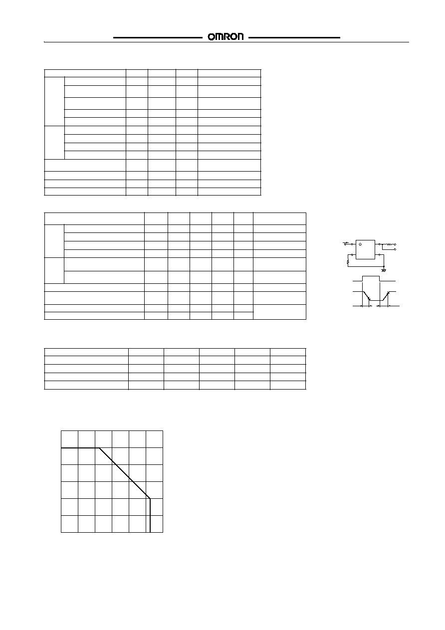
Engineering Data
Load Current vs. Ambient Temperature
G3VM-61A1(D1)
Safety Precautions
Refer to page 6 for precautions common to all G3VM models.
Item
Symbol
Rating
Unit
Measurement Conditions
Input
LED forward current
I
F
50
mA
Repetitive peak LED forward
current
I
FP
1
A
100
m
s pulses, 100 pps
LED forward current reduc-
tion rate
D I
F
/∞
C
-
0.5
mA/
∞
C
Ta
≥
25
∞
C
LED reverse voltage
V
R
5
V
Connection temperature
T
j
125
∞
C
Output
Output dielectric strength
V
OFF
60
V
Continuous load current
I
O
500
mA
ON current reduction rate
D
I
ON
/
∞
C
-
5.0
mA/
∞
C
Ta
≥
25
∞
C
Connection temperature
T
j
125
∞
C
Dielectric strength between input and
output (See note 1.)
V
I-O
2,500
Vrms
AC for 1 min
Operating temperature
T
a
-
40 to +85
∞
C
With no icing or condensation
Storage temperature
T
stg
-
55 to +125
∞
C
With no icing or condensation
Soldering temperature (10 s)
---
260
∞
C
10 s
Note:
1. The dielectric strength between the input and
output was checked by applying voltage be-
tween all pins as a group on the LED side and
all pins as a group on the light-receiving side.
Item
Symbol
Mini-
mum
Typical
Maxi-
mum
Unit
Measurement
conditions
Input
LED forward voltage
V
F
1.0
1.15
1.3
V
I
F
= 10 mA
Reverse current
I
R
---
---
10
m
A
V
R
= 5 V
Capacity between terminals
C
T
---
30
---
pF
V = 0, f = 1 MHz
Trigger LED forward current
I
FT
---
1.6
3
mA
I
O
= 500 mA
Output
Maximum resistance with output ON
R
ON
---
1
2
W
I
F
= 5 mA,
I
O
= 500 mA
Current leakage when the relay is
open
I
LEAK
---
---
1.0
m
A
V
OFF
= 60 V
Capacity between I/O terminals
C
I-O
---
0.8
---
pF
f = 1 MHz, Vs = 0 V
Insulation resistance
R
I-O
1,000
---
---
M
W
V
I-O
= 500 VDC,
RoH
£
60%
Turn-ON time
tON
---
0.8
2.0
ms
I
F
= 5 mA, R
L
= 200
W,
V
DD
= 20 V (See note 2.)
Turn-OFF time
tOFF
---
0.1
0.5
ms
10%
90%
V
OUT
I
F
t
ON
t
OFF
I
F
1
2
4
3
R
L
V
DD
V
OUT
Note:
2. Turn-ON and Turn-OFF
Times
Item
Symbol
Minimum
Typical
Maximum
Unit
Output dielectric strength
V
DD
---
---
48
V
Operating LED forward current
I
F
5
7.5
25
mA
Continuous load current
I
O
---
---
500
mA
Operating temperature
T
a
-
20
---
65
∞
C
Ambient temperature (
∞
C)
Load current (mA)
600
500
400
300
200
100
0
-
20
0
20
40
60
80
100