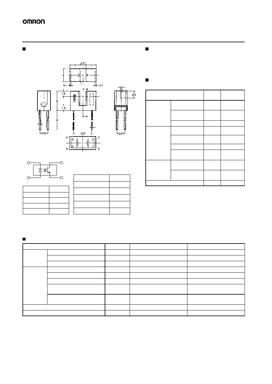
Internal Circuit
K
A
C
E
Terminal No.
Name
A
Anode
K
Cathode
C
Collector
E
Emitter
Dimensions
Tolerance
3 mm max.
±
0.3
3
t
mm
v
6
±
0.375
6
t
mm
v
10
±
0.45
10
t
mm
v
18
±
0.55
18
t
mm
v
30
±
0.65
Four, 0.5
Four, 0.25
Four, C0.3
Optical
axis
Cross section AA
Unless otherwise specified, the
tolerances are as shown below.
0.5
±
0.05
38
Photomicrosensor
(Through-beam)
EE-SX1018
Dimensions
Note:
All units are in millimeters unless otherwise indicated.
Features
∑
Compact model with a 2-mm-wide slot.
∑
PCB mounting type.
∑
High resolution with a 0.5-mm-wide slit.
Absolute Maximum Ratings
(Ta = 25
∞
C)
Item
Symbol
Rated
value
Emitter
Forward current
I
F
50 mA
(see note 1)
Pulse forward
current
I
FP
1 A
(see note 2)
Reverse voltage
V
R
4 V
Receiver
Collector≠Emitter
voltage
V
CEO
30 V
Emitter≠Collector
voltage
V
ECO
---
Collector current
I
C
20 mA
Collector
dissipation
P
C
100 mW
(see note 1)
Ambient
temperature
Operating
Topr
≠25
∞
C to
85
∞
C
Storage
Tstg
≠30
∞
C to
100
∞
C
Soldering temperature
Tsol
260
∞
C
Note:
1. Refer to the temperature rating chart if the ambient
temperature exceeds 25
∞
C.
2. The pulse width is 10
µ
s maximum with a frequency
of 100 Hz.
3. Complete soldering within 10 seconds.
Electrical and Optical Characteristics (Ta = 25
∞
C)
Item
Symbol
Value
Condition
Emitter
Forward voltage
V
F
1.2 V typ., 1.5 V max.
I
F
= 30 mA
Reverse current
I
R
0.01
µ
A typ., 10
µ
A max.
V
R
= 4 V
Peak emission wavelength
P
940 nm typ.
I
F
= 20 mA
Receiver
Light current
I
L
0.5 mA min., 14 mA max.
I
F
= 20 mA, V
CE
= 10 V
Dark current
I
D
2 nA typ., 200 nA max.
V
CE
= 10 V, 0 x
Leakage current
I
LEAK
---
---
Collector≠Emitter saturated
voltage
V
CE
(sat)
0.1 V typ., 0.4 V max.
I
F
= 20 mA, I
L
= 0.1 mA
Peak spectral sensitivity
wavelength
P
850 nm typ.
V
CE
= 10 V
Rising time
tr
4
µ
s typ.
V
CC
= 5 V, R
L
= 100
, I
L
= 5 mA
Falling time
tf
4
µ
s typ.
V
CC
= 5 V, R
L
= 100
, I
L
= 5 mA
EE-SX1018
EE-SX1018
39
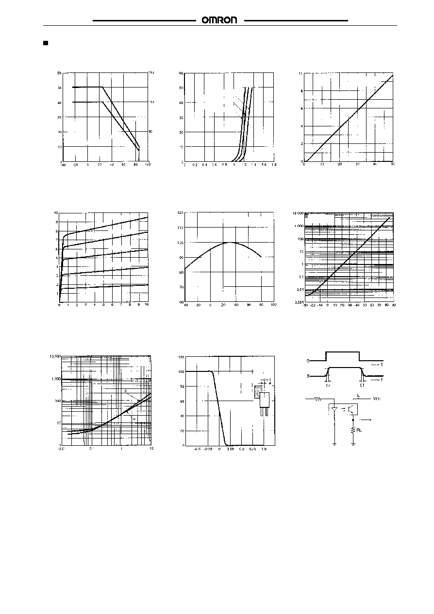
Engineering Data
Forward Current vs. Collector
Dissipation Temperature Rating
Forward Current vs. Forward
Voltage Characteristics (Typical)
Light Current vs. Forward Current
Characteristics (Typical)
Ambient temperature Ta (
∞
C)
Collector dissipation Pc (mW)
Forward voltage V
F
(V)
F
Forward current I (mA)
F
Forward current I (mA)
Forward current I
F
(mA)
Light current I (mA)
L
Light Current vs. Collector≠Emitter
Voltage Characteristics (Typical)
Relative Light Current vs. Ambi-
ent Temperature Characteristics
(Typical)
Dark Current vs. Ambient
Temperature Characteristics
(Typical)
Collector≠Emitter voltage V
CE
(V)
Light current I (mA)
L
Ambient temperature Ta (
∞
C)
Ambient temperature Ta (
∞
C)
Response Time vs. Load Resis-
tance Characteristics (Typical)
Sensing Position Characteristics
(Typical)
Response Time Measurement
Circuit
Load resistance R
L
(k
)
Distance d (mm)
I
F
= 20 mA
V
CE
= 5 V
V
CE
= 10 V
0 x
I
F
= 50 mA
I
F
= 40 mA
I
F
= 30 mA
I
F
= 20 mA
I
F
= 10 mA
I
F
= 20 mA
V
CE
= 10 V
Ta = 25
∞
C
Vcc = 5 V
Ta = 25
∞
C
(Center of
optical axis)
Input
Output
Input
Output
90 %
10 %
Ta = 25
∞
C
V
CE
= 10 V
Ta = 25
∞
C
Ta = ≠30
∞
C
Ta = 25
∞
C
Ta = 70
∞
C
Response time tr
, tf ( s)
Relative light current I (%)
L
Dark current I (nA)
D
µ
Relative light current I (%)
L
I
F
Pc