 | –≠–ª–µ–∫—Ç—Ä–æ–Ω–Ω—ã–π –∫–æ–º–ø–æ–Ω–µ–Ω—Ç: 1N5337BTA | –°–∫–∞—á–∞—Ç—å:  PDF PDF  ZIP ZIP |
©
Semiconductor Components Industries, LLC, 2004
December, 2004 - Rev. 4
1
Publication Order Number:
1N5333B/D
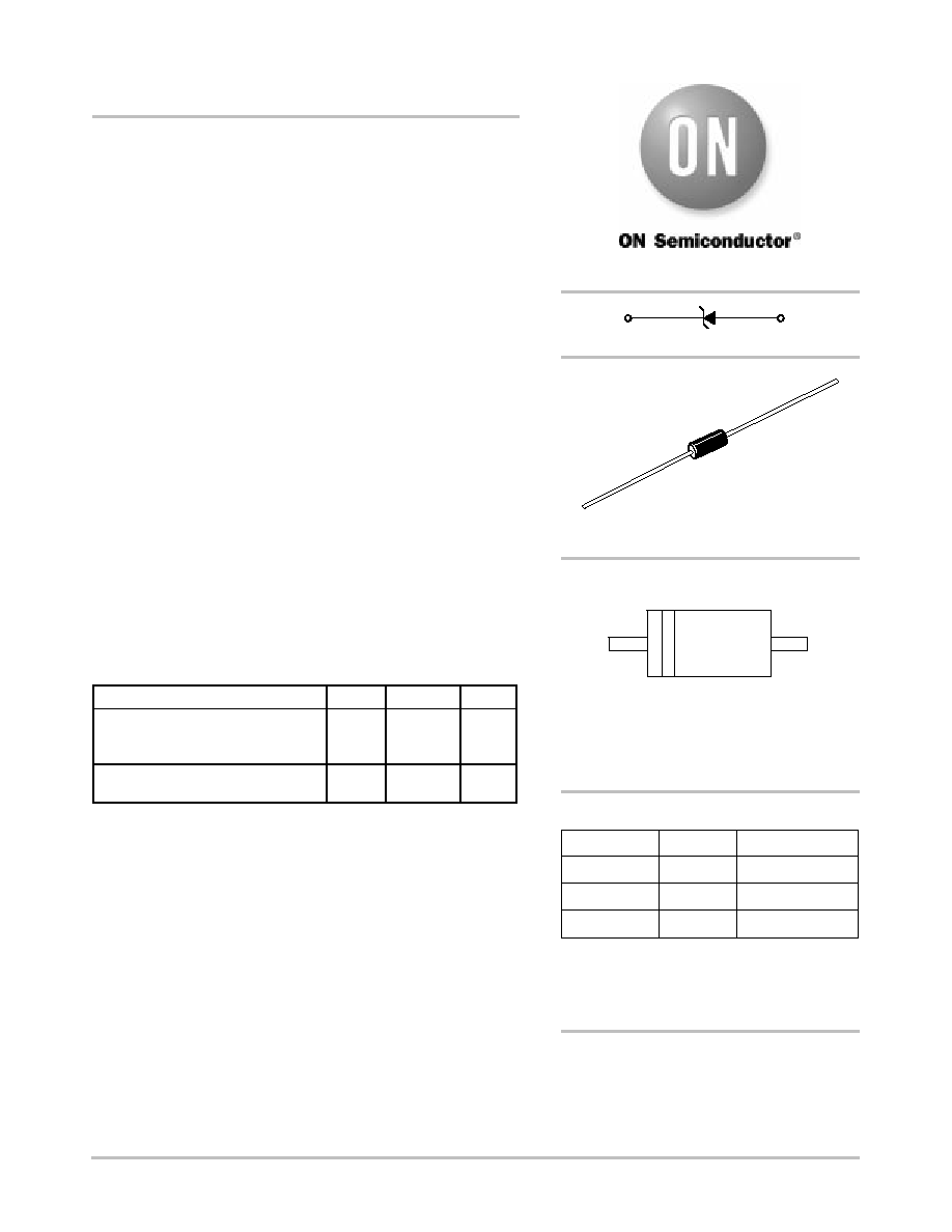
1N5333B Series
Preferred Device
5 Watt Surmetict 40
Zener Voltage Regulators
This is a complete series of 5 Watt Zener diodes with tight limits and
better operating characteristics that reflect the superior capabilities of
silicon-oxide passivated junctions. All this in an axial lead,
transfer-molded plastic package that offers protection in all common
environmental conditions.
Features
∑
Zener Voltage Range - 3.3 V to 200 V
∑
ESD Rating of Class 3 (>16 kV) per Human Body Model
∑
Surge Rating of up to 180 W @ 8.3 ms
∑
Maximum Limits Guaranteed on up to Six Electrical Parameters
∑
These devices are manufactured with a Pb-Free external lead
finish only*
Mechanical Characteristics
CASE:
Void free, transfer-molded, thermosetting plastic
FINISH:
All external surfaces are corrosion resistant and leads are
readily solderable
MAXIMUM LEAD TEMPERATURE FOR SOLDERING PURPOSES:
230
∞
C, 1/16 in. from the case for 10 seconds
POLARITY:
Cathode indicated by polarity band
MOUNTING POSITION:
Any
MAXIMUM RATINGS
Rating
Symbol
Value
Unit
Max. Steady State Power Dissipation
@ T
L
= 75
∞
C, Lead Length = 3/8 in
Derate above 75
∞
C
P
D
5
40
W
mW/
∞
C
Operating and Storage
Temperature Range
T
J
, T
stg
-65 to
+200
∞
C
Maximum ratings are those values beyond which device damage can occur.
Maximum ratings applied to the device are individual stress limit values (not
normal operating conditions) and are not valid simultaneously. If these limits
are exceeded, device functional operation is not implied, damage may occur
and reliability may be affected.
*For additional information on our Pb-Free strategy and soldering details, please
download the ON Semiconductor Soldering and Mounting Techniques
Reference Manual, SOLDERRM/D.
Device
Package
Shipping
ORDERING INFORMATION
1N53xxB
Axial Lead
1000 Units/Box
1N53xxBRL
Axial Lead
AXIAL LEAD
CASE 17
PLASTIC
4000/Tape & Reel
Cathode
Anode
L
1N
53xxB
YWW
L
= Assembly Location
1N53xxB
= Device Code
=
(See Table Next Page)
Y
= Year
WW
= Work Week
MARKING DIAGRAM
1N53xxBTA*
Axial Lead
2000/Ammo Pack
Preferred devices are recommended choices for future use
and best overall value.
*1N5361B Not Available in 2000/Ammo Pack
For information on tape and reel specifications,
including part orientation and tape sizes, please
refer to our Tape and Reel Packaging Specifications
Brochure, BRD8011/D.
http://onsemi.com
Zener Voltage Regulator
I
F
V
I
I
R
I
ZT
V
R
V
Z
V
F
1N5333B Series
http://onsemi.com
2
ELECTRICAL CHARACTERISTICS
(T
A
= 25
∞
C unless
otherwise noted, V
F
= 1.2 V Max @ I
F
= 1.0 A for all types)
Symbol
Parameter
V
Z
Reverse Zener Voltage @ I
ZT
I
ZT
Reverse Current
Z
ZT
Maximum Zener Impedance @ I
ZT
I
ZK
Reverse Current
Z
ZK
Maximum Zener Impedance @ I
ZK
I
R
Reverse Leakage Current @ V
R
V
R
Breakdown Voltage
I
F
Forward Current
V
F
Forward Voltage @ I
F
I
R
Maximum Surge Current @ T
A
= 25
∞
C
D
V
Z
Reverse Zener Voltage Change
I
ZM
Maximum DC Zener Current
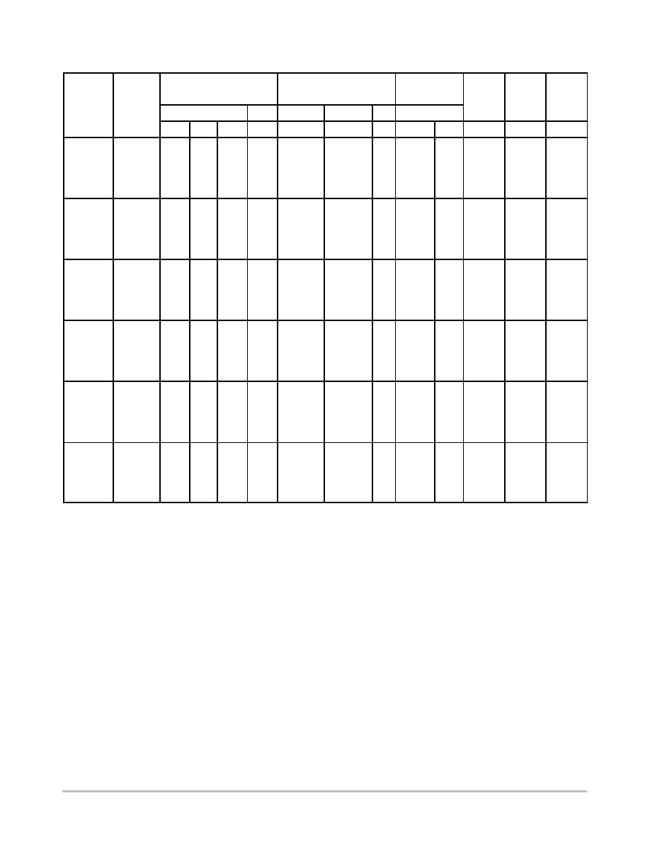
1N5333B Series
http://onsemi.com
3
ELECTRICAL CHARACTERISTICS
(T
A
= 25
∞
C unless otherwise noted, V
F
= 1.2 V Max @ I
F
= 1.0 A for all types)
Zener Voltage (Note 2)
Zener Impedance (Note 2)
Leakage
Current
I
R
D
V
Z
I
ZM
Device
Device
V
Z
(Volts)
@ I
ZT
Z
ZT
@ I
ZT
Z
ZK
@ I
ZK
I
ZK
I
R
@ V
R
I
R
(Note 3)
D
V
Z
(Note 4)
I
ZM
(Note 5)
Device
(Note 1)
Device
Marking
Min
Nom
Max
mA
W
W
mA
m
A Max
Volts
A
Volts
mA
1N5333B
1N5333B
3.14
3.3
3.47
380
3
400
1
300
1
20
0.85
1440
1N5334B
1N5334B
3.42
3.6
3.78
350
2.5
500
1
150
1
18.7
0.8
1320
1N5335B
1N5335B
3.71
3.9
4.10
320
2
500
1
50
1
17.6
0.54
1220
1N5336B
1N5336B
4.09
4.3
4.52
290
2
500
1
10
1
16.4
0.49
1100
1N5337B
1N5337B
4.47
4.7
4.94
260
2
450
1
5
1
15.3
0.44
1010
1N5338B
1N5338B
4.85
5.1
5.36
240
1.5
400
1
1
1
14.4
0.39
930
1N5339B
1N5339B
5.32
5.6
5.88
220
1
400
1
1
2
13.4
0.25
865
1N5340B
1N5340B
5.70
6.0
6.30
200
1
300
1
1
3
12.7
0.19
790
1N5341B
1N5341B
5.89
6.2
6.51
200
1
200
1
1
3
12.4
0.1
765
1N5342B
1N5342B
6.46
6.8
7.14
175
1
200
1
10
5.2
11.5
0.15
700
1N5343B
1N5343B
7.13
7.5
7.88
175
1.5
200
1
10
5.7
10.7
0.15
630
1N5344B
1N5344B
7.79
8.2
8.61
150
1.5
200
1
10
6.2
10
0.2
580
1N5345B
1N5345B
8.27
8.7
9.14
150
2
200
1
10
6.6
9.5
0.2
545
1N5346B
1N5346B
8.65
9.1
9.56
150
2
150
1
7.5
6.9
9.2
0.22
520
1N5347B
1N5347B
9.50
10
10.5
125
2
125
1
5
7.6
8.6
0.22
475
1N5348B
1N5348B
10.45
11
11.55
125
2.5
125
1
5
8.4
8.0
0.25
430
1N5349B
1N5349B
11.4
12
12.6
100
2.5
125
1
2
9.1
7.5
0.25
395
1N5350B
1N5350B
12.35
13
13.65
100
2.5
100
1
1
9.9
7.0
0.25
365
1N5351B
1N5351B
13.3
14
14.7
100
2.5
75
1
1
10.6
6.7
0.25
340
1N5352B
1N5352B
14.25
15
15.75
75
2.5
75
1
1
11.5
6.3
0.25
315
1N5353B
1N5353B
15.2
16
16.8
75
2.5
75
1
1
12.2
6.0
0.3
295
1N5354B
1N5354B
16.15
17
17.85
70
2.5
75
1
0.5
12.9
5.8
0.35
280
1N5355B
1N5355B
17.1
18
18.9
65
2.5
75
1
0.5
13.7
5.5
0.4
264
1N5356B
1N5356B
18.05
19
19.95
65
3
75
1
0.5
14.4
5.3
0.4
250
1N5357B
1N5357B
19
20
21
65
3
75
1
0.5
15.2
5.1
0.4
237
1N5358B
1N5358B
20.9
22
23.1
50
3.5
75
1
0.5
16.7
4.7
0.45
216
1N5359B
1N5359B
22.8
24
25.2
50
3.5
100
1
0.5
18.2
4.4
0.55
198
1N5360B
1N5360B
23.75
25
26.25
50
4
110
1
0.5
19
4.3
0.55
190
1N5361B*
1N5361B
25.65
27
28.35
50
5
120
1
0.5
20.6
4.1
0.6
176
1N5362B
1N5362B
26.6
28
29.4
50
6
130
1
0.5
21.2
3.9
0.6
170
Devices listed in
bold, italic are ON Semiconductor Preferred devices. Preferred devices are recommended choices for future use and best overall value.
1. TOLERANCE AND TYPE NUMBER DESIGNATION
The JEDEC type numbers shown indicate a tolerance of
±
5%.
2. ZENER VOLTAGE (V
Z
) and IMPEDANCE (I
ZT
and I
ZK
)
Test conditions for zener voltage and impedance are as follows: I
Z
is applied 40
±
10 ms prior to reading. Mounting contacts are located 3/8
to 1/2
from the inside edge of mounting clips to the body of the diode (T
A
= 25
∞
C +8
∞
C, -2
∞
C).
3. SURGE CURRENT (I
R
)
Surge current is specified as the maximum allowable peak, non-recurrent square-wave current with a pulse width, PW, of 8.3 ms. The data
given in Figure 5 may be used to find the maximum surge current for a square wave of any pulse width between 1 ms and 1000 ms by plotting
the applicable points on logarithmic paper. Examples of this, using the 3.3 V and 200 V zener are shown in Figure 6. Mounting contact located
as specified in Note 2 (T
A
= 25
∞
C +8
∞
C, -2
∞
C).
4. VOLTAGE REGULATION (
D
V
Z
)
The conditions for voltage regulation are as follows: V
Z
measurements are made at 10% and then at 50% of the I
Z
max value listed in the
electrical characteristics table. The test current time duration for each V
Z
measurement is 40
±
10 ms. Mounting contact located as specified
in Note 2 (T
A
= 25
∞
C +8
∞
C, -2
∞
C).
5. MAXIMUM REGULATOR CURRENT (I
ZM
)
The maximum current shown is based on the maximum voltage of a 5% type unit, therefore, it applies only to the B-suffix device. The actual
I
ZM
for any device may not exceed the value of 5 watts divided by the actual V
Z
of the device. T
L
= 75
∞
C at 3/8
maximum from the device
body.
*Not Available in the 2000/Ammo Pack.
1N5333B Series
http://onsemi.com
4
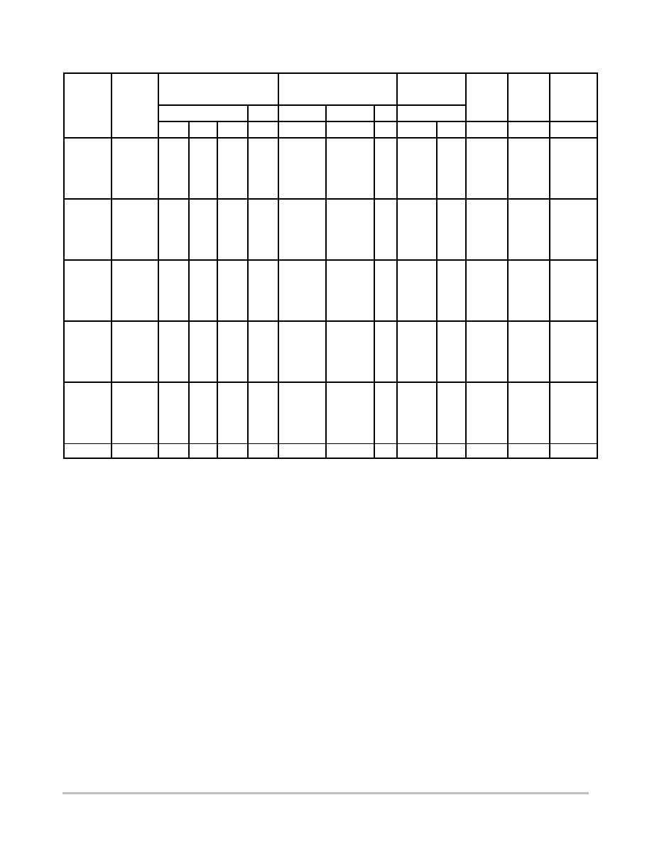
ELECTRICAL CHARACTERISTICS
(T
A
= 25
∞
C unless otherwise noted, V
F
= 1.2 V Max @ I
F
= 1.0 A for all types)
Zener Voltage (Note 7)
Zener Impedance (Note 7)
Leakage
Current
I
R
D
V
Z
I
ZM
Device
Device
V
Z
(Volts)
@ I
ZT
Z
ZT
@ I
ZT
Z
ZK
@ I
ZK
I
ZK
I
R
@ V
R
I
R
(Note 8)
D
V
Z
(Note 9)
I
ZM
(Note 10)
Device
(Note 6)
Device
Marking
Min
Nom
Max
mA
W
W
mA
m
A Max
Volts
A
Volts
mA
1N5363B
1N5363B
28.5
30
31.5
40
8
140
1
0.5
22.8
3.7
0.6
158
1N5364B
1N5364B
31.35
33
34.65
40
10
150
1
0.5
25.1
3.5
0.6
144
1N5365B
1N5365B
34.2
36
37.8
30
11
160
1
0.5
27.4
3.5
0.65
132
1N5366B
1N5366B
37.05
39
40.95
30
14
170
1
0.5
29.7
3.1
0.65
122
1N5367B
1N5367B
40.85
43
45.15
30
20
190
1
0.5
32.7
2.8
0.7
110
1N5368B
1N5368B
44.65
47
49.35
25
25
210
1
0.5
35.8
2.7
0.8
100
1N5369B
1N5369B
48.45
51
53.55
25
27
230
1
0.5
38.8
2.5
0.9
93
1N5370B
1N5370B
53.2
56
58.8
20
35
280
1
0.5
42.6
2.3
1.0
86
1N5371B
1N5371B
57
60
63
20
40
350
1
0.5
45.5
2.2
1.2
79
1N5372B
1N5372B
58.9
62
65.1
20
42
400
1
0.5
47.1
2.1
1.35
76
1N5373B
1N5373B
64.6
68
71.4
20
44
500
1
0.5
51.7
2.0
1.52
70
1N5374B
1N5374B
71.25
75
78.75
20
45
620
1
0.5
56
1.9
1.6
63
1N5375B
1N5375B
77.9
82
86.1
15
65
720
1
0.5
62.2
1.8
1.8
58
1N5376B
1N5376B
82.65
87
91.35
15
75
760
1
0.5
66
1.7
2.0
54.5
1N5377B
1N5377B
86.45
91
95.55
15
75
760
1
0.5
69.2
1.6
2.2
52.5
1N5378B
1N5378B
95
100
105
12
90
800
1
0.5
76
1.5
2.5
47.5
1N5379B
1N5379B
104.5
110
115.5
12
125
1000
1
0.5
83.6
1.4
2.5
43
1N5380B
1N5380B
114
120
126
10
170
1150
1
0.5
91.2
1.3
2.5
39.5
1N5381B
1N5381B
123.5
130
136.5
10
190
1250
1
0.5
98.8
1.2
2.5
36.6
1N5382B
1N5382B
133
140
147
8
230
1500
1
0.5
106
1.2
2.5
34
1N5383B
1N5383B
142.5
150
157.5
8
330
1500
1
0.5
114
1.1
3.0
31.6
1N5384B
1N5384B
152
160
168
8
350
1650
1
0.5
122
1.1
3.0
29.4
1N5385B
1N5385B
161.5
170
178.5
8
380
1750
1
0.5
129
1.0
3.0
28
1N5386B
1N5386B
171
180
189
5
430
1750
1
0.5
137
1.0
4.0
26.4
1N5387B
1N5387B
180.5
190
199.5
5
450
1850
1
0.5
144
0.9
5.0
25
1N5388B
1N5388B
190
200
210
5
480
1850
1
0.5
152
0.9
5.0
23.6
Devices listed in
bold, italic are ON Semiconductor Preferred devices. Preferred devices are recommended choices for future use and best overall value.
6. TOLERANCE AND TYPE NUMBER DESIGNATION
The JEDEC type numbers shown indicate a tolerance of
±
5%.
7. ZENER VOLTAGE (V
Z
) and IMPEDANCE (I
ZT
and I
ZK
)
Test conditions for zener voltage and impedance are as follows: I
Z
is applied 40
±
10 ms prior to reading. Mounting contacts are located 3/8
to 1/2
from the inside edge of mounting clips to the body of the diode (T
A
= 25
∞
C +8
∞
C, -2
∞
C).
8. SURGE CURRENT (I
R
)
Surge current is specified as the maximum allowable peak, non-recurrent square-wave current with a pulse width, PW, of 8.3 ms. The data
given in Figure 5 may be used to find the maximum surge current for a square wave of any pulse width between 1 ms and 1000 ms by plotting
the applicable points on logarithmic paper. Examples of this, using the 3.3 V and 200 V zener are shown in Figure 6. Mounting contact located
as specified in Note 7 (T
A
= 25
∞
C +8
∞
C, -2
∞
C).
9. VOLTAGE REGULATION (
D
V
Z
)
The conditions for voltage regulation are as follows: V
Z
measurements are made at 10% and then at 50% of the I
Z
max value listed in the
electrical characteristics table. The test current time duration for each V
Z
measurement is 40
±
10 ms. Mounting contact located as specified
in Note 7 (T
A
= 25
∞
C +8
∞
C, -2
∞
C).
10. MAXIMUM REGULATOR CURRENT (I
ZM
)
The maximum current shown is based on the maximum voltage of a 5% type unit, therefore, it applies only to the B-suffix device. The actual
I
ZM
for any device may not exceed the value of 5 watts divided by the actual V
Z
of the device. T
L
= 75
∞
C at 3/8
maximum from the device
body.
1N5333B Series
http://onsemi.com
5
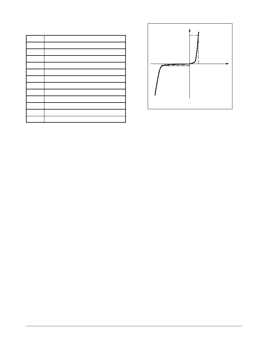
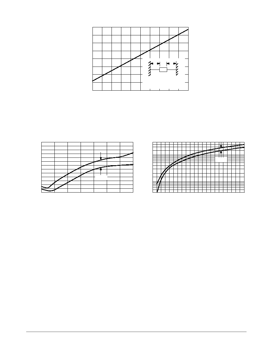
Figure 1. Typical Thermal Resistance
40
30
20
10
0
0
0.2
0.4
0.6
0.8
1
PRIMARY PATH OF
CONDUCTION IS THROUGH
THE CATHODE LEAD
L
L
L, LEAD LENGTH TO HEATSINK (INCH)
JL
, JUNCTION-T
O-LEAD
THERMAL
RESIST
ANCE (
∞
C/W)
TEMPERATURE COEFFICIENTS
Figure 2. Temperature Coefficient-Range
for Units 3 to 10 Volts
Figure 3. Temperature Coefficient-Range
for Units 10 to 220 Volts
V
Z
, ZENER VOLTAGE @ I
ZT
(VOLTS)
10
8
6
4
2
0
-2
3
4
5
6
7
8
9
10
RANGE
300
200
100
50
30
20
10
5
0
20
40
60
80 100 120 140 160 180 200 220
V
Z
, ZENER VOLTAGE @ I
ZT
(VOLTS)
V Z
, TEMPERA
TURE
COEFFICIENT
(mV/
∞
C) @ I
ZT
V Z
, TEMPERA
TURE
COEFFICIENT
(mV/
∞
C) @ I
ZT
RANGE