 | –≠–ª–µ–∫—Ç—Ä–æ–Ω–Ω—ã–π –∫–æ–º–ø–æ–Ω–µ–Ω—Ç: 1N5818 | –°–∫–∞—á–∞—Ç—å:  PDF PDF  ZIP ZIP |

©
Semiconductor Components Industries, LLC, 2005
October, 2005 - Rev. 9
1
Publication Order Number:
1N5817/D
1N5817, 1N5818, 1N5819
1N5817 and 1N5819 are Preferred Devices
Axial Lead Rectifiers
This series employs the Schottky Barrier principle in a large area
metal-to-silicon power diode. State-of-the-art geometry features
chrome barrier metal, epitaxial construction with oxide passivation
and metal overlap contact. Ideally suited for use as rectifiers in
low-voltage, high-frequency inverters, free wheeling diodes, and
polarity protection diodes.
Features
∑
Extremely Low V
F
∑
Low Stored Charge, Majority Carrier Conduction
∑
Low Power Loss/High Efficiency
∑
Lead Temperature for Soldering Purposes:
260
∞C Max for 10 Seconds
∑
These are Pb-Free Devices
Mechanical Characteristics
∑
Case: Epoxy, Molded
∑
Weight: 0.4 Gram (Approximately)
∑
Finish: All External Surfaces Corrosion Resistant and Terminal
Leads are Readily Solderable
∑
Polarity: Cathode Indicated by Polarity Band
∑
ESD Ratings: Machine Model = C (>400 V)
Human Body Model = 3B (>8000 V)
*For additional information on our Pb-Free strategy and soldering details, please
download the ON Semiconductor Soldering and Mounting Techniques
Reference Manual, SOLDERRM/D.
AXIAL LEAD
CASE 59-10
DO-41
PLASTIC
SCHOTTKY BARRIER
RECTIFIERS
1.0 AMPERE
20, 30 and 40 VOLTS
Preferred devices are recommended choices for future use
and best overall value.
MARKING DIAGRAM
See detailed ordering and shipping information on page 2 of
this data sheet.
ORDERING INFORMATION
http://onsemi.com
A
= Assembly Location
1N581x = Device Number
x = 7, 8, or 9
YY
= Year
WW
= Work Week
G
= Pb-Free Package
A
1N581x
YYWW
G
G
(Note: Microdot may be in either location)

1N5817, 1N5818, 1N5819
http://onsemi.com
2
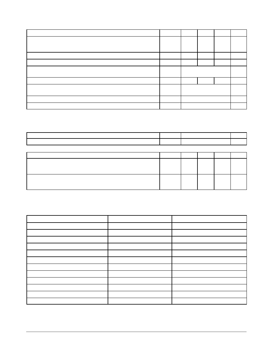
MAXIMUM RATINGS
Rating
Symbol
1N5817
1N5818
1N5819
Unit
Peak Repetitive Reverse Voltage
Working Peak Reverse Voltage
DC Blocking Voltage
V
RRM
V
RWM
V
R
20
30
40
V
Non-Repetitive Peak Reverse Voltage
V
RSM
24
36
48
V
RMS Reverse Voltage
V
R(RMS)
14
21
28
V
Average Rectified Forward Current (Note 1), (V
R(equiv)
0.2 V
R
(dc), T
L
= 90
∞
C,
R
q
JA
= 80
∞
C/W, P.C. Board Mounting, see Note 2, T
A
= 55
∞
C)
I
O
1.0
A
Ambient Temperature (Rated V
R
(dc), P
F(AV)
= 0, R
q
JA
= 80
∞
C/W)
T
A
85
80
75
∞
C
Non-Repetitive Peak Surge Current, (Surge applied at rated load conditions,
half-wave, single phase 60 Hz, T
L
= 70
∞
C)
I
FSM
25 (for one cycle)
A
Operating and Storage Junction Temperature Range (Reverse Voltage applied)
T
J
, T
stg
-65 to +125
∞
C
Peak Operating Junction Temperature (Forward Current applied)
T
J(pk)
150
∞
C
Maximum ratings are those values beyond which device damage can occur. Maximum ratings applied to the device are individual stress limit
values (not normal operating conditions) and are not valid simultaneously. If these limits are exceeded, device functional operation is not implied,
damage may occur and reliability may be affected.
THERMAL CHARACTERISTICS
(Note 1)
Characteristic
Symbol
Max
Unit
Thermal Resistance, Junction-to-Ambient
R
q
JA
80
∞
C/W
ELECTRICAL CHARACTERISTICS
(T
L
= 25
∞
C unless otherwise noted) (Note 1)
Characteristic
Symbol
1N5817
1N5818
1N5819
Unit
Maximum Instantaneous Forward Voltage (Note 2)
(i
F
= 0.1 A)
(i
F
= 1.0 A)
(i
F
= 3.0 A)
v
F
0.32
0.45
0.75
0.33
0.55
0.875
0.34
0.6
0.9
V
Maximum Instantaneous Reverse Current @ Rated dc Voltage (Note 2)
(T
L
= 25
∞
C)
(T
L
= 100
∞
C)
I
R
1.0
10
1.0
10
1.0
10
mA
1. Lead Temperature reference is cathode lead 1/32 in from case.
2. Pulse Test: Pulse Width = 300
m
s, Duty Cycle = 2.0%.
ORDERING INFORMATION
Device
Package
Shipping
1N5817
Axial Lead*
1000 Units / Bag
1N5817G
Axial Lead*
1000 Units / Bag
1N5817RL
Axial Lead*
5000 / Tape & Reel
1N5817RLG
Axial Lead*
5000 / Tape & Reel
1N5818
Axial Lead*
1000 Units / Bag
1N5818G
Axial Lead*
1000 Units / Bag
1N5818RL
Axial Lead*
5000 / Tape & Reel
1N5818RLG
Axial Lead*
5000 / Tape & Reel
1N5819
Axial Lead*
1000 Units / Bag
1N5819G
Axial Lead*
1000 Units / Bag
1N5819RL
Axial Lead*
5000 / Tape & Reel
1N5819RLG
Axial Lead*
5000 / Tape & Reel
For information on tape and reel specifications, including part orientation and tape sizes, please refer to our Tape and Reel Packaging
Specifications Brochure, BRD8011/D.
*This package is inherently Pb-Free.

125
115
105
95
85
75
20
15
10
7.0
5.0
4.0
3.0
2.0
T R
, REFERENCE
TEMPERA
TURE (
∞
C)
V
R
, DC REVERSE VOLTAGE (VOLTS)
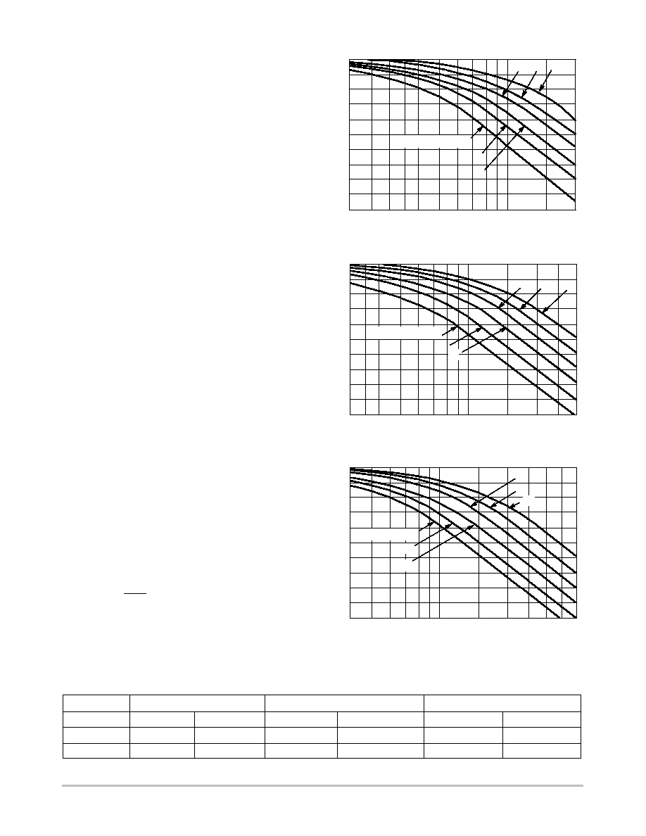
Figure 1. Maximum Reference Temperature
1N5817
40
30
23
60
80
R
qJA
(∞C/W) = 110
125
115
105
95
85
75
20
15
10
7.0
5.0
30
4.0
3.0
40
30
23
R
qJA
(∞C/W) = 110
80
60
Figure 2. Maximum Reference Temperature
1N5818
125
115
105
95
85
75
20
15
10
7.0
5.0
30
4.0
40
R
qJA
(∞C/W) = 110
60
80
Figure 3. Maximum Reference Temperature
1N5819
40
30
23
T R
, REFERENCE
TEMPERA
TURE (
C
)
∞
V
R
, DC REVERSE VOLTAGE (VOLTS)
V
R
, DC REVERSE VOLTAGE (VOLTS)
T R
, REFERENCE
TEMPERA
TURE (
∞
C)
1N5817, 1N5818, 1N5819
http://onsemi.com
3
NOTE 1. -- DETERMINING MAXIMUM RATINGS
Reverse power dissipation and the possibility of thermal
runaway must be considered when operating this rectifier at
reverse voltages above 0.1 V
RWM
. Proper derating may be
accomplished by use of equation (1).
T
A(max)
=
where T
A(max)
=
T
J(max)
=
P
F(AV)
=
P
R(AV)
=
R
q
JA
=
T
J(max)
- R
q
JA
P
F(AV)
- R
q
JA
P
R(AV)
Maximum allowable ambient temperature
Maximum allowable junction temperature
(1)
Average forward power dissipation
(125
∞
C or the temperature at which thermal
runaway occurs, whichever is lowest)
Average reverse power dissipation
Junction-to-ambient thermal resistance
Figures 1, 2, and 3 permit easier use of equation (1) by
taking reverse power dissipation and thermal runaway into
consideration. The figures solve for a reference temperature
as determined by equation (2).
T
R
= T
J(max)
- R
q
JA
P
R(AV)
(2)
Substituting equation (2) into equation (1) yields:
T
A(max)
= T
R
- R
q
JA
P
F(AV)
(3)
Inspection of equations (2) and (3) reveals that T
R
is the
ambient temperature at which thermal runaway occurs or
where T
J
= 125
∞C, when forward power is zero. The
transition from one boundary condition to the other is
evident on the curves of Figures 1, 2, and 3 as a difference
in the rate of change of the slope in the vicinity of 115
∞C. The
data of Figures 1, 2, and 3 is based upon dc conditions. For
use in common rectifier circuits, Table 1 indicates suggested
factors for an equivalent dc voltage to use for conservative
design, that is:
(4)
V
R(equiv)
= V
in(PK)
x F
The factor F is derived by considering the properties of the
various rectifier circuits and the reverse characteristics of
Schottky diodes.
EXAMPLE: Find T
A(max)
for 1N5818 operated in a
12-volt dc supply using a bridge circuit with capacitive filter
such that I
DC
= 0.4 A (I
F(AV)
= 0.5 A), I
(FM)
/I
(AV)
= 10, Input
Voltage = 10 V
(rms)
, R
qJA
= 80
∞C/W.
Step 1. Find V
R(equiv)
. Read F = 0.65 from Table 1,
Step 1. Find
V
R(equiv)
= (1.41)(10)(0.65) = 9.2 V.
Step 2. Find T
R
from Figure 2. Read T
R
= 109
∞
C
Step 1. Find
@ V
R
= 9.2 V and R
q
JA
= 80
∞
C/W.
Step 3. Find P
F(AV)
from Figure 4. **Read P
F(AV)
= 0.5 W
@
I
(FM)
I
(AV)
= 10 and IF(AV) = 0.5 A.
Step 4. Find T
A(max)
from equation (3).
Step 4. Find
T
A(max)
= 109 - (80) (0.5) = 69
∞
C.
**Values given are for the 1N5818. Power is slightly lower for the
1N5817 because of its lower forward voltage, and higher for the
1N5819.
Circuit
Load
Half Wave
Resistive
Capacitive*
Full Wave, Bridge
Resistive
Capacitive
Full Wave, Center Tapped*
Resistive
Capacitive
Sine Wave
Square Wave
0.5
0.75
1.3
1.5
0.5
0.75
0.65
0.75
1.0
1.5
1.3
1.5
**Note that V
R(PK)
2.0 V
in(PK)
.
Use line to center tap voltage for V
in
.
Table 1. Values for Factor F

1N5817, 1N5818, 1N5819
http://onsemi.com
4
7/8
20
40
50
90
80
70
60
30
10
3/4
5/8
1/2
3/8
1/4
1.0
1/8
1
R
JL
, THERMAL
RESIST
ANCE,
JUNCTION-T
O-LEAD
( ∞
C/W)
BOTH LEADS TO HEATSINK,
EQUAL LENGTH
MAXIMUM
TYPICAL
L, LEAD LENGTH (INCHES)
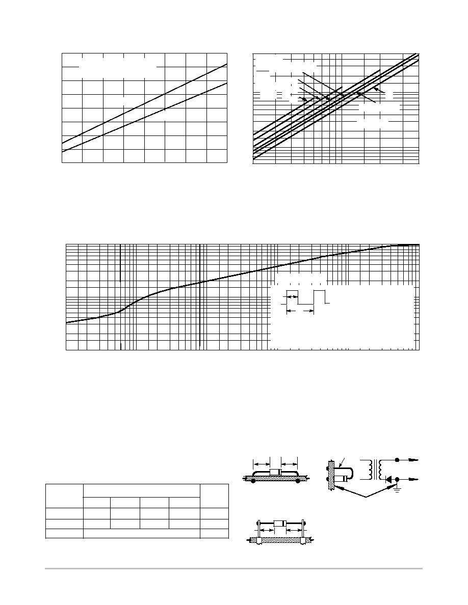
Figure 4. Steady-State Thermal Resistance
5.0
3.0
2.0
1.0
0.7
0.5
0.3
0.2
0.1
0.07
0.05
4.0
2.0
1.0
0.8
0.6
0.4
0.2
P F(A
V)
,
A
VERAGE POWER DISSIP
A
T
ION (W
A
TTS)
I
F(AV)
, AVERAGE FORWARD CURRENT (AMP)
dc
SQUARE WAVE
T
J
125∞C
1.0
0.7
0.5
0.3
0.2
0.1
0.07
0.05
0.03
0.02
0.01
10k
2.0k
1.0k
500
200
100
50
20
10
5.0
2.0
1.0
0.5
0.2
0.1
5.0k
r(t), TRANSIENT
THERMAL
RESIST
ANCE
(NORMALIZED)
Z
qJL(t)
= Z
qJL
∑ r(t)
P
pk
P
pk
t
p
t
1
TIME
DUTY CYCLE, D = t
p
/t
1
PEAK POWER, P
pk
, is peak of
an
equivalent square power pulse.
D
T
JL
= P
pk
∑
R
q
JL
[D + (1 - D)
∑
r(t
1
+ t
p
) + r(t
p
) - r(t
1
)] where
D
T
JL
= the increase in junction temperature above the lead temperature
r(t) = normalized value of transient thermal resistance at time, t, from Figure 6,
i.e.:
r(t) =
r(t
1
+ t
p
) = normalized value of transient thermal resistance at time, t
1
+ t
p
.
t, TIME (ms)
NOTE 2. -- MOUNTING DATA
Data shown for thermal resistance junction-to-ambient
(R
qJA
) for the mountings shown is to be used as typical guide-
line values for preliminary engineering, or in case the tie
point temperature cannot be measured.
TYPICAL VALUES FOR R
q
JA
IN STILL AIR
Mounting
Method
1/8
1/4
1/2
3/4
Lead Length, L (in)
R
q
JA
1
2
3
52
67
65
80
72
87
85
100
∞
C/W
∞
C/W
∞
C/W
50
Mounting Method 1
P.C. Board with
1-1/2
x 1-1/2
copper surface.
Mounting Method 3
P.C. Board with
1-1/2
x 1-1/2
copper surface.
L
L
L = 3/8
BOARD GROUND
PLANE
VECTOR PIN MOUNTING
L
L
Mounting Method 2
5
10
20
Sine Wave
I
(FM)
I
(AV)
= (Resistive Load)
Capacitive
Loads
{
Figure 5. Forward Power Dissipation
1N5817-19
Figure 6. Thermal Response

1N5817, 1N5818, 1N5819
http://onsemi.com
5
100
70
5.0
30
20
10
7.0
5.0
3.0
20
7.0
10
3.0
2.0
30
1.0
40
15
5.0
3.0
2.0
0.3
0.2
0.1
40
36
12
30
20
1.0
0.5
0.05
0.03
24
16
20
8.0
4.0
28
0
32
10
20
7.0
5.0
2.0
0.2
0.3
0.5
0.7
1.0
3.0
0.9
1.0 1.1
0.1
0.07
0.05
0.03
0.02
0.6
0.5
0.4
0.3
0.2
0.7
0.1
0.8
NOTE 3. -- THERMAL CIRCUIT MODEL
(For heat conduction through the leads)
T
A(A)
T
A(K)
R
qS(A)
R
qL(A)
R
qJ(A)
R
qJ(K)
R
qL(K)
R
qS(K)
P
D
T
L(A)
T
C(A)
T
J
T
C(K)
T
L(K)
v
F
, INSTANTANEOUS FORWARD VOLTAGE (VOLTS)
i F
, INST
ANT
ANEOUS FOR
W
ARD CURRENT
(AMP)
Figure 7. Typical Forward Voltage
I FSM
, PEAK SURGE CURRENT
(AMP)
NUMBER OF CYCLES
Figure 8. Maximum Non-Repetitive Surge Current
I R
, REVERSE CURRENT
(mA)
V
R
, REVERSE VOLTAGE (VOLTS)
Figure 9. Typical Reverse Current
T
C
= 100∞C
25∞C
1 Cycle
T
L
= 70
∞
C
f = 60 Hz
Surge Applied at
Rated Load Conditions
1N5817
1N5818
1N5819
T
J
= 125∞C
100∞C
25∞C
Use of the above model permits junction to lead thermal re-
sistance for any mounting configuration to be found. For a
given total lead length, lowest values occur when one side of
the rectifier is brought as close as possible to the heatsink.
Terms in the model signify:
T
A
= Ambient Temperature
T
C
= Case Temperature
T
L
= Lead Temperature
T
J
= Junction Temperature
R
q
S
= Thermal Resistance, Heatsink to Ambient
R
q
L
= Thermal Resistance, Lead to Heatsink
R
q
J
= Thermal Resistance, Junction to Case
P
D
= Power Dissipation
(Subscripts A and K refer to anode and cathode sides, re-
spectively.) Values for thermal resistance components are:
R
q
L
= 100
∞
C/W/in typically and 120
∞
C/W/in maximum
R
q
J
= 36
∞
C/W typically and 46
∞
C/W maximum.
75∞C

