 | –≠–ª–µ–∫—Ç—Ä–æ–Ω–Ω—ã–π –∫–æ–º–ø–æ–Ω–µ–Ω—Ç: 1N5917BRL | –°–∫–∞—á–∞—Ç—å:  PDF PDF  ZIP ZIP |
©
Semiconductor Components Industries, LLC, 2002
February, 2002 ≠ Rev. 2
1
Publication Order Number:
1N5913B/D
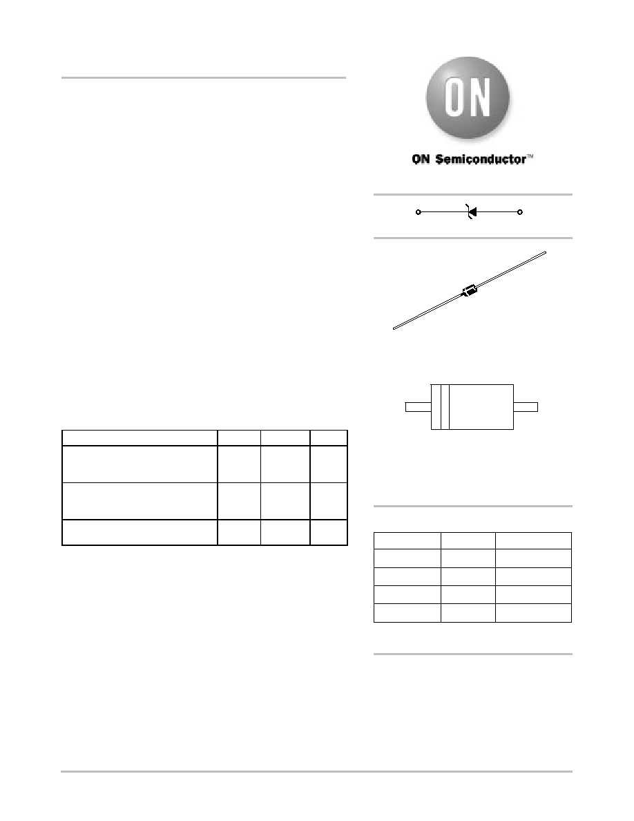
1N5913B Series
3 Watt DO-41 SurmeticE 30
Zener Voltage Regulators
This is a complete series of 3 Watt Zener diodes with limits and
excellent operating characteristics that reflect the superior capabilities
of silicon≠oxide passivated junctions. All this in an axial≠lead,
transfer≠molded plastic package that offers protection in all common
environmental conditions.
Specification Features:
∑
Zener Voltage Range ≠ 3.3 V to 200 V
∑
ESD Rating of Class 3 (>16 KV) per Human Body Model
∑
Surge Rating of 98 W @ 1 ms
∑
Maximum Limits Guaranteed on up to Six Electrical Parameters
∑
Package No Larger than the Conventional 1 Watt Package
Mechanical Characteristics:
CASE:
Void free, transfer≠molded, thermosetting plastic
FINISH:
All external surfaces are corrosion resistant and leads are
readily solderable
MAXIMUM LEAD TEMPERATURE FOR SOLDERING PURPOSES:
230
∞
C, 1/16
from the case for 10 seconds
POLARITY:
Cathode indicated by polarity band
MOUNTING POSITION:
Any
MAXIMUM RATINGS
Rating
Symbol
Value
Unit
Max. Steady State Power Dissipation
@ T
L
= 75
∞
C, Lead Length = 3/8
Derate above 75
∞
C
P
D
3
24
W
mW/
∞
C
Steady State Power Dissipation
@ T
A
= 50
∞
C
Derate above 50
∞
C
P
D
1
6.67
W
mW/
∞
C
Operating and Storage
Temperature Range
T
J
, T
stg
≠65 to
+200
∞
C
Device
Package
Shipping
ORDERING INFORMATION
1N59xxB
Axial Lead
2000 Units/Box
1N59xxBRL
Axial Lead
AXIAL LEAD
CASE 59
PLASTIC
http://onsemi.com
6000/Tape & Reel
Cathode
Anode
{
Polarity band up with cathode lead off first
}
Polarity band down with cathode lead off first
L
1N59
xxB
YYWW
L
= Assembly Location
1N59xxB
= Device Code
=
(See Table Next Page)
YY
= Year
WW
= Work Week
MARKING DIAGRAM
1N59xxBRR1
{
Axial Lead
2000/Tape & Reel
1N59xxBRR2
}
Axial Lead
2000/Tape & Reel
Devices listed in
bold, italic are ON Semiconductor
Preferred devices. Preferred devices are recommended
choices for future use and best overall value.
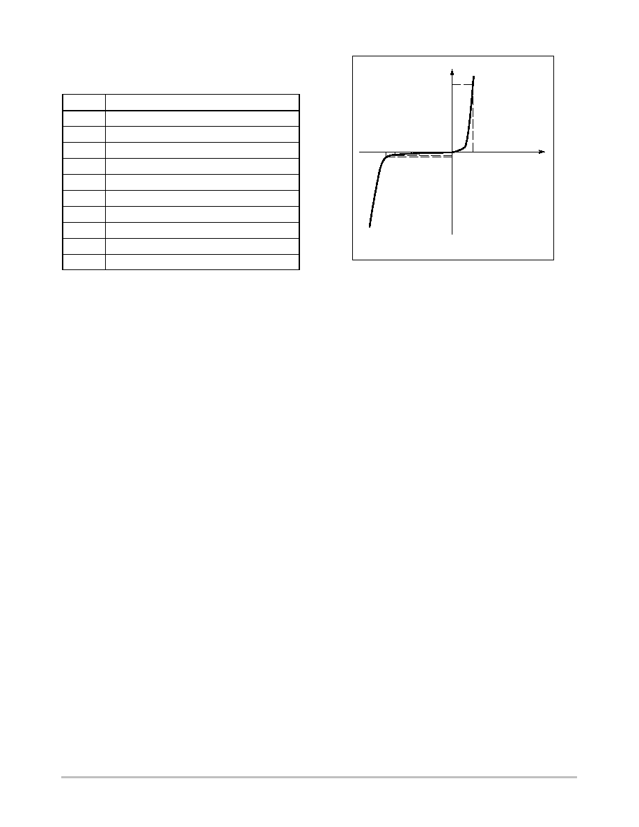
Zener Voltage Regulator
I
F
V
I
I
R
I
ZT
V
R
V
Z
V
F
1N5913B Series
http://onsemi.com
2
ELECTRICAL CHARACTERISTICS
(T
L
= 30
∞
C unless otherwise noted,
V
F
= 1.5 V Max @ I
F
= 200 mAdc for all types)
Symbol
Parameter
V
Z
Reverse Zener Voltage @ I
ZT
I
ZT
Reverse Current
Z
ZT
Maximum Zener Impedance @ I
ZT
I
ZK
Reverse Current
Z
ZK
Maximum Zener Impedance @ I
ZK
I
R
Reverse Leakage Current @ V
R
V
R
Breakdown Voltage
I
F
Forward Current
V
F
Forward Voltage @ I
F
I
ZM
Maximum DC Zener Current
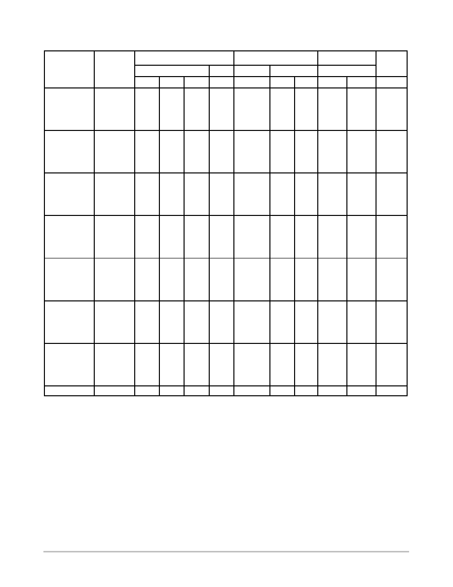
1N5913B Series
http://onsemi.com
3
ELECTRICAL CHARACTERISTICS
(T
L
= 30
∞
C unless otherwise noted, V
F
= 1.5 V Max @ I
F
= 200 mAdc for all types)
Zener Voltage (Note 2)
Zener Impedance (Note 3)
Leakage Current
Device
Device
V
Z
(Volts)
@ I
ZT
Z
ZT
@ I
ZT
Z
ZK
@ I
ZK
I
R
@ V
R
I
ZM
Device
(Note 1)
Device
Marking
Min
Nom
Max
mA
W
W
mA
µ
A Max
Volts
mA
1N5913B
1N5913B
3.14
3.3
3.47
113.6
10
500
1
100
1
454
1N5917B
1N5917B
4.47
4.7
4.94
79.8
5
500
1
5
1.5
319
1N5919B
1N5919B
5.32
5.6
5.88
66.9
2
250
1
5
3
267
1N5920B
1N5920B
5.89
6.2
6.51
60.5
2
200
1
5
4
241
1N5921B
1N5921B
6.46
6.8
7.14
55.1
2.5
200
1
5
5.2
220
1N5923B
1N5923B
7.79
8.2
8.61
45.7
3.5
400
0.5
5
6.5
182
1N5924B
1N5924B
8.65
9.1
9.56
41.2
4
500
0.5
5
7
164
1N5925B
1N5925B
9.50
10
10.50
37.5
4.5
500
0.25
5
8
150
1N5926B
1N5926B
10.45
11
11.55
34.1
5.5
550
0.25
1
8.4
136
1N5927B
1N5927B
11.40
12
12.60
31.2
6.5
550
0.25
1
9.1
125
1N5929B
1N5929B
14.25
15
15.75
25.0
9
600
0.25
1
11.4
100
1N5930B
1N5930B
15.20
16
16.80
23.4
10
600
0.25
1
12.2
93
1N5931B
1N5931B
17.10
18
18.90
20.8
12
650
0.25
1
13.7
83
1N5932B
1N5932B
19.00
20
21.00
18.7
14
650
0.25
1
15.2
75
1N5933B
1N5933B
20.90
22
23.10
17.0
17.5
650
0.25
1
16.7
68
1N5934B
1N5934B
22.80
24
25.20
15.6
19
700
0.25
1
18.2
62
1N5935B
1N5935B
25.65
27
28.35
13.9
23
700
0.25
1
20.6
55
1N5936B
1N5936B
28.50
30
31.50
12.5
28
750
0.25
1
22.8
50
1N5937B
1N5937B
31.35
33
34.65
11.4
33
800
0.25
1
25.1
45
1N5938B
1N5938B
34.20
36
37.80
10.4
38
850
0.25
1
27.4
41
1N5940B
1N5940B
40.85
43
45.15
8.7
53
950
0.25
1
32.7
34
1N5941B
1N5941B
44.65
47
49.35
8.0
67
1000
0.25
1
35.8
31
1N5942B
1N5942B
48.45
51
53.55
7.3
70
1100
0.25
1
38.8
29
1N5943B
1N5943B
53.20
56
58.80
6.7
86
1300
0.25
1
42.6
26
1N5944B
1N5944B
58.90
62
65.10
6.0
100
1500
0.25
1
47.1
24
1N5945B
1N5945B
64.60
68
71.40
5.5
120
1700
0.25
1
51.7
22
1N5946B
1N5946B
71.25
75
78.75
5.0
140
2000
0.25
1
56
20
1N5947B
1N5947B
77.90
82
86.10
4.6
160
2500
0.25
1
62.2
18
1N5948B
1N5948B
86.45
91
95.55
4.1
200
3000
0.25
1
69.2
16
1N5950B
1N5950B
104.5
110
115.5
3.4
300
4000
0.25
1
83.6
13
1N5951B
1N5951B
114
120
126
3.1
380
4500
0.25
1
91.2
12
1N5952B
1N5952B
123.5
130
136.5
2.9
450
5000
0.25
1
98.8
11
1N5953B
1N5953B
142.5
150
157.5
2.5
600
6000
0.25
1
114
10
1N5954B
1N5954B
152
160
168
2.3
700
6500
0.25
1
121.6
9
1N5955B
1N5955B
171
180
189
2.1
900
7000
0.25
1
136.8
8
1N5956B
1N5956B
190
200
210
1.9
1200
8000
0.25
1
152
7
1. TOLERANCE AND TYPE NUMBER DESIGNATION
Tolerance designation ≠ device tolerance of
±
5% are indicated by a "B" suffix.
2. ZENER VOLTAGE (V
Z
) MEASUREMENT
ON Semiconductor guarantees the zener voltage when measured at 90 seconds while maintaining the lead temperature (T
L
) at 30
∞
C
±
1
∞
C,
3/8
from the diode body.
3. ZENER IMPEDANCE (Z
Z
) DERIVATION
The zener impedance is derived from 60 seconds AC voltage, which results when an AC current having an rms value equal to 10% of the
DC zener current (I
ZT
or I
ZK
) is superimposed on I
ZT
or I
ZK
.
1N5913B Series
http://onsemi.com
4
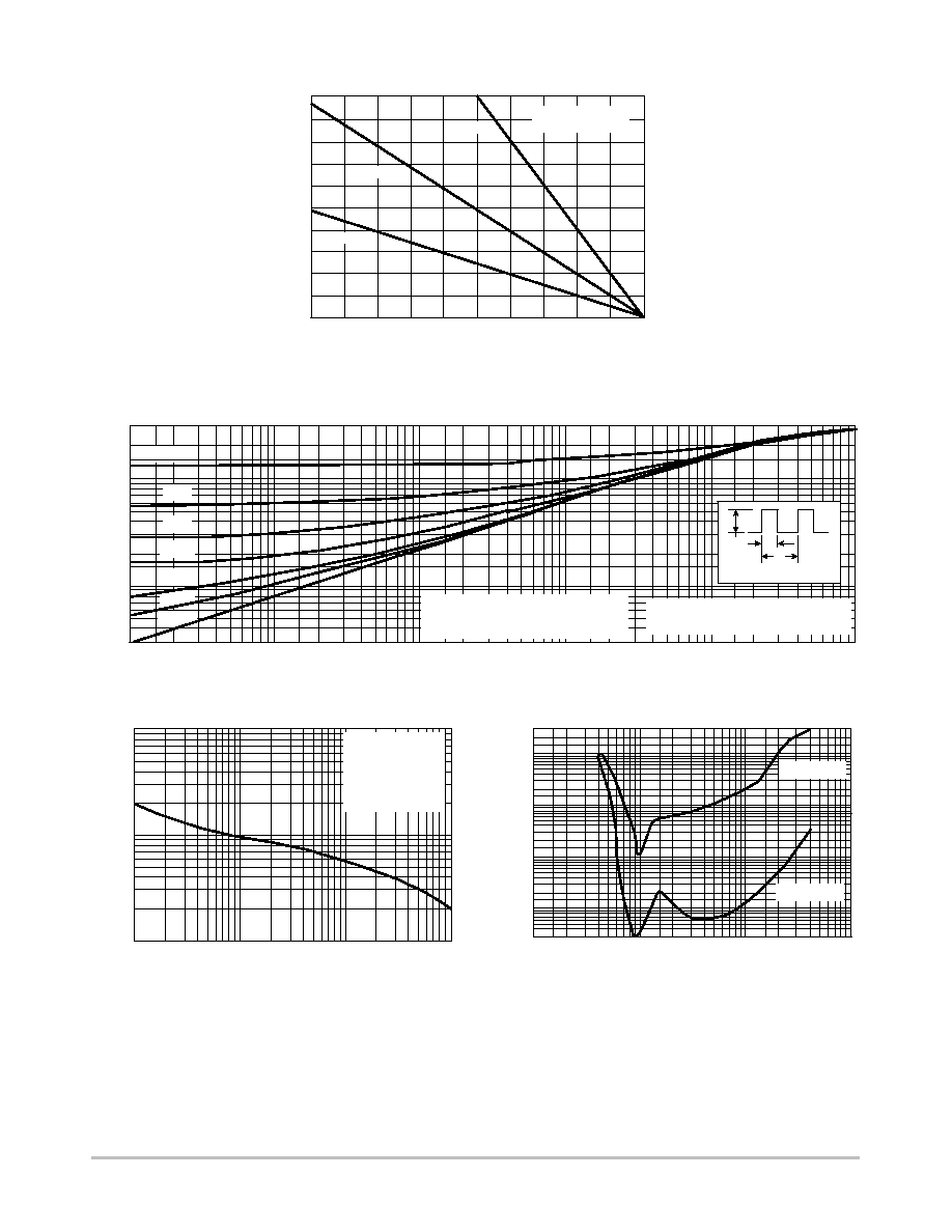
Figure 1. Power Temperature Derating Curve
T
L
, LEAD TEMPERATURE (
∞
C)
0
20
40
60
200
80
100
120 140 160 180
0
1
2
3
4
5
L = 1/8
L = 3/8
L = 1
L = LEAD LENGTH
TO HEAT SINK
P
D
, STEADY ST
A
TE DISSIP
A
TION (W
A
TTS)
t, TIME (SECONDS)
0.0001 0.0002
0.0005
0.001
0.002
0.005
0.01
0.02
0.05
0.1
0.2
0.5
1
2
5
10
0.3
0.5
0.7
1
2
3
5
7
10
20
30
D =0.5
0.2
0.1
0.05
0.01
D = 0
DUTY CYCLE, D =t
1
/t
2
JL
(t, D)
TRANSIENT
THERMAL
RESIST
ANCE
JUNCTIONT
OLEAD ( C/W)
∞
P
PK
t
1
NOTE: BELOW 0.1 SECOND, THERMAL
RESPONSE CURVE IS APPLICABLE
TO ANY LEAD LENGTH (L).
SINGLE PULSE
T
JL
=
JL
(t)P
PK
REPETITIVE PULSES
T
JL
=
JL
(t,D)P
PK
t
2
0.02
10
20
30
50
100
200
300
500
1K
0.1
0.2 0.3 0.5
1
2 3
5
10
20 30 50 100
PW, PULSE WIDTH (ms)
P
, PEAK SURGE POWER (W
A
TTS)
PK
1
2
5
10
20
50
100 200 400 1000
0.0003
0.0005
0.001
0.002
0.005
0.01
0.02
0.05
0.1
0.2
0.5
1
2
3
T
A
= 125
∞
C
T
A
= 125
∞
C
NOMINAL V
Z
(VOLTS)
AS SPECIFIED IN ELEC. CHAR.
T
ABLE
Figure 2. Typical Thermal Response L, Lead Length = 3/8 Inch
Figure 3. Maximum Surge Power
Figure 4. Typical Reverse Leakage
I R
, REVERSE LEAKAGE (
µ
Adc) @ V
R
RECTANGULAR
NONREPETITIVE
WAVEFORM
T
J
= 25
∞
C PRIOR
TO INITIAL PULSE

1N5913B Series
http://onsemi.com
5
APPLICATION NOTE
Since the actual voltage available from a given zener
diode is temperature dependent, it is necessary to determine
junction temperature under any set of operating conditions
in order to calculate its value. The following procedure is
recommended:
Lead Temperature, T
L
, should be determined from:
T
L
=
LA
P
D
+ T
A
LA
is the lead-to-ambient thermal resistance (
∞
C/W) and P
D
is the power dissipation. The value for
LA
will vary and
depends on the device mounting method.
LA
is generally
30≠40
∞
C/W for the various clips and tie points in common
use and for printed circuit board wiring.
The temperature of the lead can also be measured using a
thermocouple placed on the lead as close as possible to the
tie point. The thermal mass connected to the tie point is
normally large enough so that it will not significantly
respond to heat surges generated in the diode as a result of
pulsed operation once steady-state conditions are achieved.
Using the measured value of T
L
, the junction temperature
may be determined by:
T
J
= T
L
+
T
JL
T
JL
is the increase in junction temperature above the lead
temperature and may be found from Figure 2 for a train of
power pulses (L = 3/8 inch) or from Figure 10 for dc power.
T
JL
=
JL
P
D
For worst-case design, using expected limits of I
Z
, limits
of P
D
and the extremes of T
J
(
T
J
) may be estimated.
Changes in voltage, V
Z
, can then be found from:
V =
VZ
T
J
VZ
, the zener voltage temperature coefficient, is found
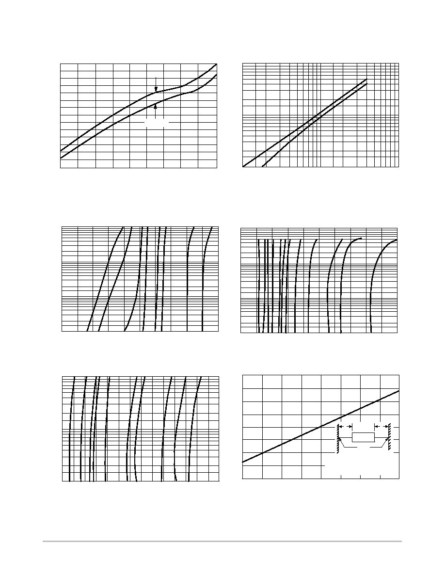
from Figures 5 and 6.
Under high power-pulse operation, the zener voltage will
vary with time and may also be affected significantly by the
zener resistance. For best regulation, keep current
excursions as low as possible.
Data of Figure 2 should not be used to compute surge
capability. Surge limitations are given in Figure 3. They are
lower than would be expected by considering only junction
temperature, as current crowding effects cause temperatures
to be extremely high in small spots resulting in device
degradation should the limits of Figure 3 be exceeded.
1N5913B Series
http://onsemi.com
6
Figure 5. Units To 12 Volts
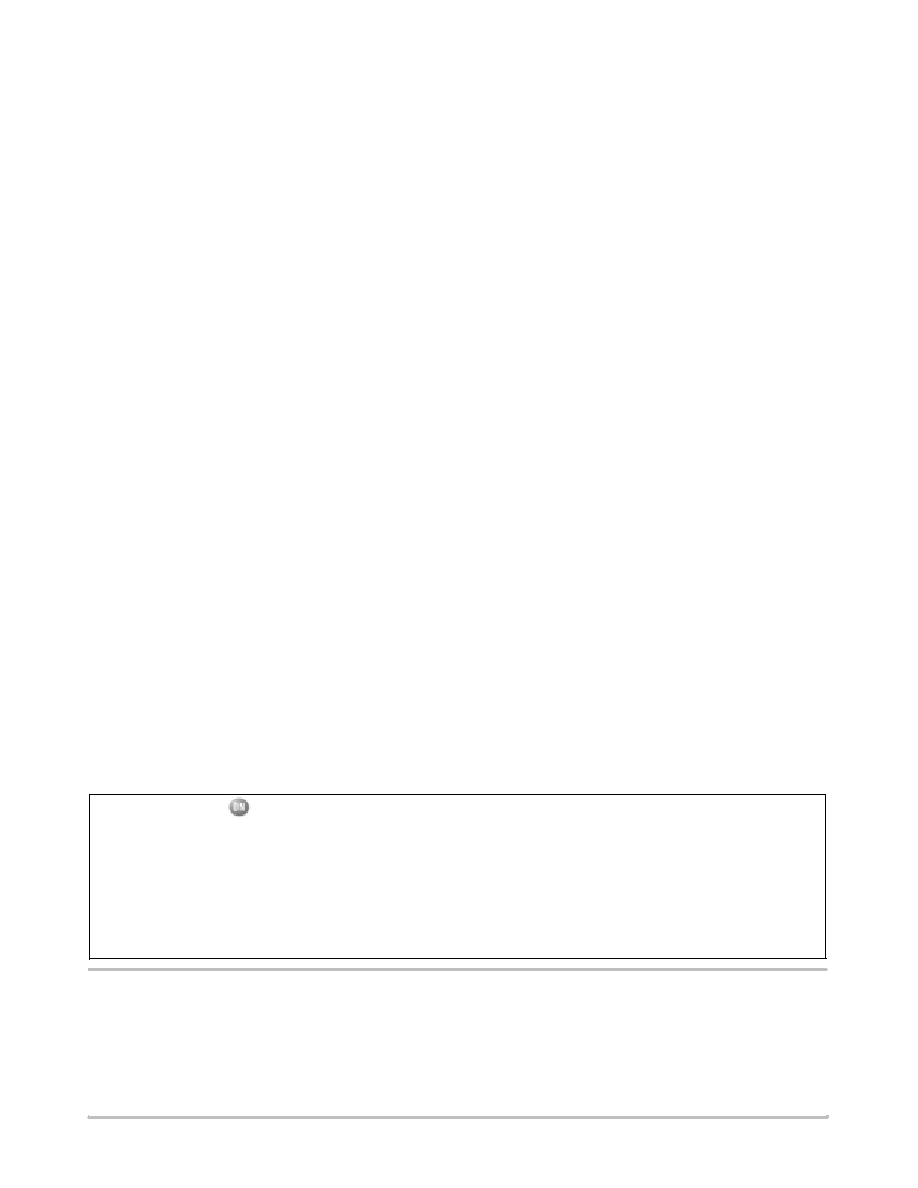
Figure 6. Units 10 To 400 Volts
Figure 7. V
Z
= 3.3 thru 10 Volts
Figure 8. V
Z
= 12 thru 82 Volts
Figure 9. V
Z
= 100 thru 400 Volts
Figure 10. Typical Thermal Resistance
ZENER VOLTAGE versus ZENER CURRENT
(Figures 7, 8 and 9)
TEMPERATURE COEFFICIENT RANGES
(90% of the Units are in the Ranges Indicated)
V
Z
, ZENER VOLTAGE @ I
ZT
(VOLTS)
3
4
5
6
7
8
9
10
11
12
10
8
6
4
2
0
-2
-4
RANGE
,
TEMPERA
TURE COEFFICIENT
(mV/ C) @ I
ZT
VZ
∞
1000
500
200
100
50
20
10
10
20
50
100
200
400
1000
V
Z
, ZENER VOLTAGE @ I
ZT
(VOLTS)
,
TEMPERA
TURE COEFFICIENT
(mV/ C) @ I
ZT
VZ
∞
0
1
2
3
4
5
6
7
8
9
10
100
50
30
20
10
1
0.5
0.3
0.2
0.1
V
Z
, ZENER VOLTAGE (VOLTS)
I , ZENER CURRENT
(mA)
Z
2
5
3
0
10
20
30
40
50
60
70
80
90
100
V
Z
, ZENER VOLTAGE (VOLTS)
I , ZENER CURRENT
(mA)
Z
100
50
30
20
10
1
0.5
0.3
0.2
0.1
2
5
3
100
200
300
400
250
350
150
10
1
0.5
0.2
0.1
V
Z
, ZENER VOLTAGE (VOLTS)
2
5
I , ZENER CURRENT
(mA)
Z
0
10
20
30
40
50
60
70
80
L, LEAD LENGTH TO HEAT SINK (INCH)
PRIMARY PATH OF
CONDUCTION IS THROUGH
THE CATHODE LEAD
0
1/8
1/4
3/8
1/2
5/8
3/4
7/8
1
T
L
JL
, JUNCTIONT
OLEAD
THERMAL
RESIST
ANCE
L
L
( C/W)
∞

1N5913B Series
http://onsemi.com
7
OUTLINE DIMENSIONS
3 Watt DO≠41 Surmetic
E
30
Zener Voltage Regulators ≠ Axial Leaded
PLASTIC DO≠41
CASE 59≠10
ISSUE R
B
D
K
K
F
F
A
DIM
MIN
MAX
MIN
MAX
MILLIMETERS
INCHES
A
4.10
5.20
0.161
0.205
B
2.00
2.70
0.079
0.106
D
0.71
0.86
0.028
0.034
F
---
1.27
---
0.050
K
25.40
---
1.000
---
NOTES:
1. DIMENSIONING AND TOLERANCING PER ANSI
Y14.5M, 1982.
2. CONTROLLING DIMENSION: INCH.
3. 59-04 OBSOLETE, NEW STANDARD 59-09.
4. 59-03 OBSOLETE, NEW STANDARD 59-10.
5. ALL RULES AND NOTES ASSOCIATED WITH
JEDEC DO-41 OUTLINE SHALL APPLY
6. POLARITY DENOTED BY CATHODE BAND.
7. LEAD DIAMETER NOT CONTROLLED WITHIN F
DIMENSION.
1N5913B Series
http://onsemi.com
8
ON Semiconductor and are trademarks of Semiconductor Components Industries, LLC (SCILLC). SCILLC reserves the right to make changes
without further notice to any products herein. SCILLC makes no warranty, representation or guarantee regarding the suitability of its products for any particular
purpose, nor does SCILLC assume any liability arising out of the application or use of any product or circuit, and specifically disclaims any and all liability,
including without limitation special, consequential or incidental damages. "Typical" parameters which may be provided in SCILLC data sheets and/or
specifications can and do vary in different applications and actual performance may vary over time. All operating parameters, including "Typicals" must be
validated for each customer application by customer's technical experts. SCILLC does not convey any license under its patent rights nor the rights of others.
SCILLC products are not designed, intended, or authorized for use as components in systems intended for surgical implant into the body, or other applications
intended to support or sustain life, or for any other application in which the failure of the SCILLC product could create a situation where personal injury or
death may occur. Should Buyer purchase or use SCILLC products for any such unintended or unauthorized application, Buyer shall indemnify and hold
SCILLC and its officers, employees, subsidiaries, affiliates, and distributors harmless against all claims, costs, damages, and expenses, and reasonable
attorney fees arising out of, directly or indirectly, any claim of personal injury or death associated with such unintended or unauthorized use, even if such claim
alleges that SCILLC was negligent regarding the design or manufacture of the part. SCILLC is an Equal Opportunity/Affirmative Action Employer.
PUBLICATION ORDERING INFORMATION
JAPAN: ON Semiconductor, Japan Customer Focus Center
4≠32≠1 Nishi≠Gotanda, Shinagawa≠ku, Tokyo, Japan 141≠0031
Phone: 81≠3≠5740≠2700
Email: r14525@onsemi.com
ON Semiconductor Website: http://onsemi.com
For additional information, please contact your local
Sales Representative.
1N5913B/D
Surmetic is a trademark of Semiconductor Components Industries, LLC.
Literature Fulfillment:
Literature Distribution Center for ON Semiconductor
P.O. Box 5163, Denver, Colorado 80217 USA
Phone: 303≠675≠2175 or 800≠344≠3860 Toll Free USA/Canada
Fax: 303≠675≠2176 or 800≠344≠3867 Toll Free USA/Canada
Email: ONlit@hibbertco.com
N. American Technical Support: 800≠282≠9855 Toll Free USA/Canada