 | –≠–ª–µ–∫—Ç—Ä–æ–Ω–Ω—ã–π –∫–æ–º–ø–æ–Ω–µ–Ω—Ç: 2N5401ZL1 | –°–∫–∞—á–∞—Ç—å:  PDF PDF  ZIP ZIP |

©
Semiconductor Components Industries, LLC, 2004
May, 2004 - Rev. 1
1
Publication Order Number:
2N5401/D
2N5401
Preferred Device
Amplifier Transistors
PNP Silicon
Features
∑
Pb-Free Packages are Available*
MAXIMUM RATINGS
Rating
Symbol
2N5400
2N5401
Unit
Collector - Emitter Voltage
V
CEO
120
150
Vdc
Collector - Base Voltage
V
CBO
130
160
Vdc
Emitter - Base Voltage
V
EBO
5.0
Vdc
Collector Current - Continuous
I
C
600
mAdc
Total Device Dissipation
@ T
A
= 25
∞
C
Derate above 25
∞
C
P
D
625
5.0
mW
mW/
∞
C
Total Device Dissipation
@ T
C
= 25
∞
C
Derate above 25
∞
C
P
D
1.5
12
Watts
mW/
∞
C
Operating and Storage Junction
Temperature Range
T
J
, T
stg
-55 to +150
∞
C
Maximum ratings are those values beyond which device damage can occur.
Maximum ratings applied to the device are individual stress limit values (not nor-
mal operating conditions) and are not valid simultaneously. If these limits are ex-
ceeded, device functional operation is not implied, damage may occur and reli-
ability may be affected.
THERMAL CHARACTERISTICS
Characteristic
Symbol
Max
Unit
Thermal Resistance,
Junction-to-Ambient
R
q
JA
200
∞
C/W
Thermal Resistance,
Junction-to-Case
R
q
JC
83.3
∞
C/W
2N54xx
Y
= Year
WW
= Work Week
YWW
MARKING DIAGRAM
TO-92
CASE 29
STYLE 1
1 2
3
Preferred devices are recommended choices for future use
and best overall value.
See detailed ordering and shipping information in the package
dimensions section on page 2 of this data sheet.
ORDERING INFORMATION
http://onsemi.com
*For additional information on our Pb-Free strategy
and soldering details, please download the
ON Semiconductor Soldering and Mounting
Techniques Reference Manual, SOLDERRM/D.
COLLECTOR
3
2
BASE
1
EMITTER

2N5401
http://onsemi.com
2
ELECTRICAL CHARACTERISTICS
(T
A
= 25
∞
C unless otherwise noted)
Characteristic
Symbol
Min
Max
Unit
OFF CHARACTERISTICS
Collector-Emitter Breakdown Voltage
(1)
(I
C
= 1.0 mAdc, I
B
= 0)
2N5400
2N5401
V
(BR)CEO
150
-
Vdc
Collector-Base Breakdown Voltage
(I
C
= 100
m
Adc, I
E
= 0)
2N5400
2N5401
V
(BR)CBO
160
-
Vdc
Emitter-Base Breakdown Voltage
(I
E
= 10
m
Adc, I
C
= 0)
V
(BR)EBO
5.0
-
Vdc
Collector Cutoff Current
(V
CB
= 120 Vdc, I
E
= 0)
2N5401
(V
CB
= 120 Vdc, I
E
= 0, T
A
= 100
∞
C)
2N5401
I
CBO
-
-
50
50
Emitter Cutoff Current
(V
EB
= 3.0 Vdc, I
C
= 0)
I
EBO
-
50
nAdc
ON CHARACTERISTICS (Note 1)
DC Current Gain
(I
C
= 1.0 mAdc, V
CE
= 5.0 Vdc)
(I
C
= 10 mAdc, V
CE
= 5.0 Vdc)
(I
C
= 50 mAdc, V
CE
= 5.0 Vdc)
h
FE
50
60
50
-
240
-
-
Collector-Emitter Saturation Voltage
(I
C
= 10 mAdc, I
B
= 1.0 mAdc)
(I
C
= 50 mAdc, I
B
= 5.0 mAdc)
V
CE(sat)
-
-
0.2
0.5
Vdc
Base-Emitter Saturation Voltage
(I
C
= 10 mAdc, I
B
= 1.0 mAdc)
(I
C
= 50 mAdc, I
B
= 5.0 mAdc)
V
BE(sat)
-
-
1.0
1.0
Vdc
SMALL-SIGNAL CHARACTERISTICS
Current-Gain -- Bandwidth Product
(I
C
= 10 mAdc, V
CE
= 10 Vdc, f = 100 MHz)
f
T
100
300
MHz
Output Capacitance
(V
CB
= 10 Vdc, I
E
= 0, f = 1.0 MHz)
C
obo
-
6.0
pF
Small-Signal Current Gain
(I
C
= 1.0 mAdc, V
CE
= 10 Vdc, f = 1.0 kHz)
h
fe
40
200
-
Noise Figure
(I
C
= 250
m
Adc, V
CE
= 5.0 Vdc, R
S
= 1.0 k
W
, f = 1.0 kHz)
NF
-
8.0
dB
1. Pulse Test: Pulse Width
300
m
s, Duty Cycle
2.0%.
ORDERING INFORMATION
Device
Package
Shipping
2N5401
TO-92
5000 Unit / Bulk
2N5401RL1
TO-92
2000 Tape & Reel
2N5401RLRA
TO-92
2000 Tape & Reel
2N5401RLRAG
TO-92
(Pb-Free)
2000 Tape & Reel
2N5401RLRM
TO-92
2000 Tape & Ammo Box
2N5401ZL1
TO-92
2000 Tape & Ammo Box
For information on tape and reel specifications, including part orientation and tape sizes, please refer to our Tape and Reel Packaging Specifica-
tions Brochure, BRD8011/D.

2N5401
http://onsemi.com
3
Figure 1. DC Current Gain
I
C
, COLLECTOR CURRENT (mA)
30
100
150
200
0.1
h , CURRENT GAIN
0.5
2.0
3.0
10
0.2
0.3
20
1.0
5.0
FE
T
J
= 125
∞
C
25
∞
C
-55
∞
C
70
50
20
30
50
100
V
CE
= - 1.0 V
V
CE
= - 5.0 V
Figure 2. Collector Saturation Region
I
B
, BASE CURRENT (mA)
1.0
0.1
0.5
2.0
10
0.2
1.0
5.0
20
50
0.9
0.8
0.7
0.6
0.5
0.4
0.3
0.2
0.1
0
0.005
0.01
0.02
0.05
Figure 3. Collector Cut-Off Region
V
BE
, BASE-EMITTER VOLTAGE (VOLTS)
V CE
, COLLECTOR-EMITTER VOL
T
AGE (VOL
TS)
, COLLECTOR CURRENT (A)
µ
I C
10
3
0.1
0.3
0.2
10
2
10
1
10
0
10
-1
10
-2
10
-3
0
0.1
0.2
0.3
0.4
0.5
0.6
0.7
I
C
= 1.0 mA
10 mA
30 mA
100 mA
V
CE
= 30 V
I
C
= I
CES
T
J
= 125
∞
C
75
∞
C
25
∞
C
REVERSE
FORWARD

2N5401
http://onsemi.com
4
Figure 4. "On" Voltages
I
C
, COLLECTOR CURRENT (mA)
0.4
0.6
0.7
1.0
0.2
Figure 5. Temperature Coefficients
I
C
, COLLECTOR CURRENT (mA)
V
,
VOL
T
AGE (VOL
TS)
0
T
J
= 25
∞
C
V
CE(sat)
@ I
C
/I
B
= 10
2.5
0.1
0.2
0.5
1.0
2.0
5.0
10
20
50
100
C, CAP
ACIT
ANCE (pF)
100
T
J
= 25
∞
C
C
ibo
Figure 6. Switching Time Test Circuit
V
R
, REVERSE VOLTAGE (VOLTS)
0.9
0.8
0.5
0.3
0.1
V
BE(sat)
@ I
C
/I
B
= 10
0.3
3.0
30
V, TEMPERA
TURE COEFFICIENT (mV/
C)
∞
Figure 7. Capacitances
10.2 V
V
in
10 ms
INPUT PULSE
V
BB
+8.8 V
100
R
B
5.1 k
0.25 mF
V
in
100
1N914
V
out
R
C
V
CC
-30 V
3.0 k
t
r
, t
f
10 ns
DUTY CYCLE = 1.0%
Values Shown are for I
C
@ 10 mA
0.1
0.2
0.5
1.0
2.0
5.0
10
20
50
100
0.3
3.0
30
2.0
1.5
1.0
0.5
0
-0.5
-1.0
-1.5
-2.0
-2.5
T
J
= - 55
∞
C to 135
∞
C
q
VC
for V
CE(sat)
q
VB
for V
BE(sat)
C
obo
1.0
2.0
3.0
5.0
7.0
10
20
30
50
70
0.2
0.5
1.0
2.0
5.0
10
20
0.3
3.0
0.7
7.0
t, TIME (ns)
1000
100
200
300
500
700
10
20
30
50
70
0.2
0.5
1.0
2.0
5.0
10
20
0.3
3.0
30 50
100
200
I
C
, COLLECTOR CURRENT (mA)
Figure 8. Turn-On Time
I
C
/I
B
= 10
T
J
= 25
∞
C
t
d
@ V
BE(off)
= 1.0 V
V
CC
= 120 V
t
r
@ V
CC
= 30 V
t
r
@ V
CC
= 120 V
t, TIME (ns)
2000
100
200
300
500
700
20
30
50
70
0.2
0.5
1.0
2.0
5.0
10
20
0.3
3.0
30 50
100
200
I
C
, COLLECTOR CURRENT (mA)
Figure 9. Turn-Off Time
1000
t
f
@ V
CC
= 120 V
t
f
@ V
CC
= 30 V
t
s
@ V
CC
= 120 V
I
C
/I
B
= 10
T
J
= 25
∞
C
2N5401
http://onsemi.com
5
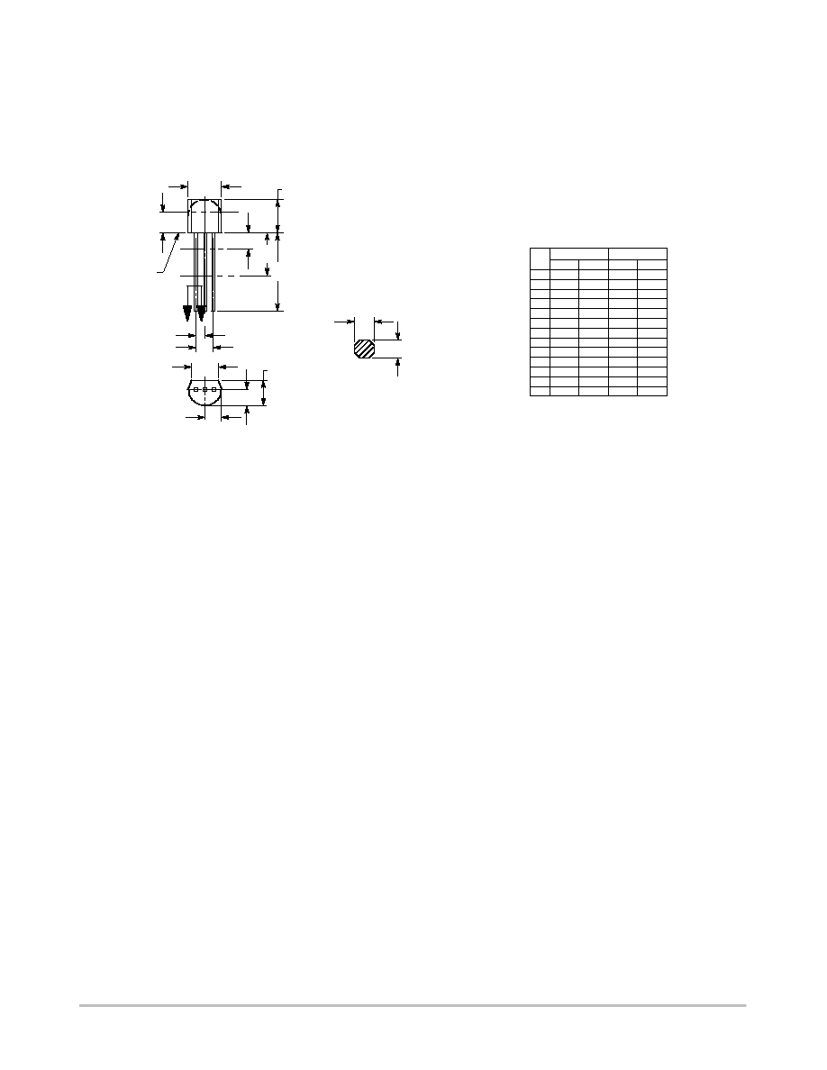
PACKAGE DIMENSIONS
STYLE 1:
PIN 1. EMITTER
2. BASE
3. COLLECTOR
TO-92
CASE 29-11
ISSUE AL
NOTES:
1. DIMENSIONING AND TOLERANCING PER ANSI
Y14.5M, 1982.
2. CONTROLLING DIMENSION: INCH.
3. CONTOUR OF PACKAGE BEYOND DIMENSION R
IS UNCONTROLLED.
4. LEAD DIMENSION IS UNCONTROLLED IN P AND
BEYOND DIMENSION K MINIMUM.
R
A
P
J
L
B
K
G
H
SECTION X-X
C
V
D
N
N
X X
SEATING
PLANE
DIM
MIN
MAX
MIN
MAX
MILLIMETERS
INCHES
A
0.175
0.205
4.45
5.20
B
0.170
0.210
4.32
5.33
C
0.125
0.165
3.18
4.19
D
0.016
0.021
0.407
0.533
G
0.045
0.055
1.15
1.39
H
0.095
0.105
2.42
2.66
J
0.015
0.020
0.39
0.50
K
0.500
---
12.70
---
L
0.250
---
6.35
---
N
0.080
0.105
2.04
2.66
P
---
0.100
---
2.54
R
0.115
---
2.93
---
V
0.135
---
3.43
---
1