 | –≠–ª–µ–∫—Ç—Ä–æ–Ω–Ω—ã–π –∫–æ–º–ø–æ–Ω–µ–Ω—Ç: 2N6344 | –°–∫–∞—á–∞—Ç—å:  PDF PDF  ZIP ZIP |
©
Semiconductor Components Industries, LLC, 1999
March, 2000 ≠ Rev. 1
1
Publication Order Number:
2N6344/D
2N6344, 2N6349
Preferred Device
Triacs
Silicon Bidirectional Thyristors
Designed primarily for full-wave ac control applications, such as
light dimmers, motor controls, heating controls and power supplies; or
wherever full≠wave silicon gate controlled solid≠state devices are
needed. Triac type thyristors switch from a blocking to a conducting
state for either polarity of applied main terminal voltage with positive
or negative gate triggering.
∑
Blocking Voltage to 800 Volts
∑
All Diffused and Glass Passivated Junctions for Greater Parameter
Uniformity and Stability
∑
Small, Rugged, Thermowatt Construction for Low Thermal
Resistance, High Heat Dissipation and Durability
∑
Gate Triggering Guaranteed in all Four Quadrants
∑
For 400 Hz Operation, Consult Factory
∑
Device Marking: Logo, Device Type, e.g., 2N6344, Date Code
MAXIMUM RATINGS
(TJ = 25
∞
C unless otherwise noted)
Rating
Symbol
Value
Unit
* Peak Repetitive Off≠State Voltage(1)
(TJ = ≠40 to +110
∞
C, Sine Wave 50 to
60 Hz, Gate Open)
2N6344
2N6349
VDRM,
VRRM
600
800
Volts
*On≠State RMS Current
(TC = +80
∞
C)
Full Cycle Sine Wave 50 to 60 Hz
(TC = +90
∞
C)
IT(RMS)
8.0
4.0
Amps
*Peak Non≠Repetitive Surge Current
(One Full Cycle, Sine Wave 60 Hz,
TC = +25
∞
C)
Preceded and followed by rated current
ITSM
100
Amps
Circuit Fusing Consideration (t = 8.3 ms)
I2t
40
A2s
*Peak Gate Power
(TC = +80
∞
C, Pulse Width = 2
µ
s)
PGM
20
Watts
*Average Gate Power
(TC = +80
∞
C, t = 8.3 ms)
PG(AV)
0.5
Watt
*Peak Gate Current
(TC = +80
∞
C, Pulse Width = 2.0
µ
s)
IGM
2.0
Amps
*Peak Gate Voltage
(TC = +80
∞
C, Pulse Width = 2.0
µ
s)
VGM
10
Volts
*Operating Junction Temperature Range
TJ
≠ 40 to
+125
∞
C
*Storage Temperature Range
Tstg
≠ 40 to
+150
∞
C
(1) VDRM and VRRM for all types can be applied on a continuous basis. Blocking
voltages shall not be tested with a constant current source such that the
voltage ratings of the devices are exceeded.
TRIACS
8 AMPERES RMS
600 thru 800 VOLTS
Device
Package
Shipping
ORDERING INFORMATION
2N6344
TO220AB
500/Box
2N6349
TO220AB
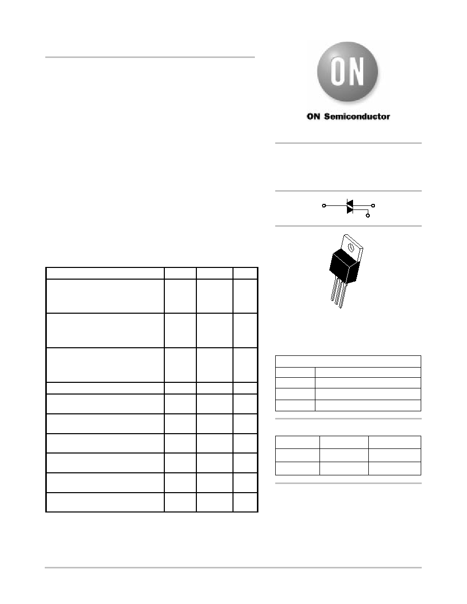
TO≠220AB
CASE 221A
STYLE 4
1
2
3
4
PIN ASSIGNMENT
1
2
3
Gate
Main Terminal 1
Main Terminal 2
4
Main Terminal 2
http://onsemi.com
500/Box
MT1
G
MT2
Preferred devices are recommended choices for future use
and best overall value.

2N6344, 2N6349
http://onsemi.com
2
THERMAL CHARACTERISTICS
Characteristic
Symbol
Max
Unit
*Thermal Resistance, Junction to Case
R
JC
2.2
∞
C/W
Maximum Lead Temperature for Soldering Purposes 1/8
from Case for 10 Seconds
TL
260
∞
C
ELECTRICAL CHARACTERISTICS
(TC = 25
∞
C unless otherwise noted; Electricals apply in both directions)
Characteristic
Symbol
Min
Typ
Max
Unit
OFF CHARACTERISTICS
* Peak Repetitive Blocking Current
(VD = Rated VDRM, VRRM; Gate Open)
TJ = 25
∞
C
TJ = 100
∞
C
IDRM,
IRRM
--
--
--
--
10
2.0
µ
A
mA
ON CHARACTERISTICS
* Peak On≠State Voltage
(ITM =
"
11 A Peak; Pulse Width = 1 to 2 ms, Duty Cycle
p
2%)
VTM
--
1.3
1.55
Volts
Gate Trigger Current (Continuous dc)
(VD = 12 Vdc, RL = 100 Ohms)
MT2(+), G(+)
MT2(+), G(≠)
MT2(≠), G(≠)
MT2(≠), G(+)
*MT2(+), G(+); MT2(≠), G(≠) TC = ≠40
∞
C
*MT2(+), G(≠); MT2(≠), G(+) TC = ≠40
∞
C
IGT
--
--
--
--
--
--
12
12
20
35
--
--
50
75
50
75
100
125
mA
Gate Trigger Voltage (Continuous dc)
(VD = 12 Vdc, RL = 100 Ohms)
MT2(+), G(+)
MT2(+), G(≠)
MT2(≠), G(≠)
MT2(≠), G(+)
*MT2(+), G(+); MT2(≠), G(≠) TC = ≠40
∞
C
*MT2(+), G(≠); MT2(≠), G(+) TC = ≠40
∞
C
VGT
--
--
--
--
--
--
0.9
0.9
1.1
1.4
--
--
2.0
2.5
2.0
2.5
2.5
3.0
Volts
Gate Non≠Trigger Voltage (Continuous dc)
(VD = Rated VDRM, RL = 10 k Ohms, TJ = 100
∞
C)
*MT2(+), G(+); MT2(≠), G(≠); MT2(+), G(≠); MT2(≠), G(≠)
VGD
0.2
--
--
Volts
* Holding Current
(VD = 12 Vdc, Gate Open)
TC = 25
∞
C
(Initiating Current =
"
200 mA)
*TC = ≠40
∞
C
IH
--
--
6.0
--
40
75
mA
* Turn-On Time
(VD = Rated VDRM, ITM = 11 A, IGT = 120 mA,
Rise Time = 0.1
µ
s, Pulse Width = 2
µ
s)
tgt
--
1.5
2.0
µ
s
DYNAMIC CHARACTERISTICS
Critical Rate of Rise of Commutation Voltage
(VD = Rated VDRM, ITM = 11 A, Commutating di/dt = 4.0 A/ms,
Gate Unenergized, TC = 80
∞
C)
dv/dt(c)
--
5.0
--
V/
µ
s
*Indicates JEDEC Registered Data.

2N6344, 2N6349
http://onsemi.com
3
+ Current
+ Voltage
VTM
IH
Symbol
Parameter
VDRM
Peak Repetitive Forward Off State Voltage
IDRM
Peak Forward Blocking Current
VRRM
Peak Repetitive Reverse Off State Voltage
IRRM
Peak Reverse Blocking Current
Voltage Current Characteristic of Triacs
(Bidirectional Device)
IDRM at VDRM
on state
off state
IRRM at VRRM
Quadrant 1
MainTerminal 2 +
Quadrant 3
MainTerminal 2 ≠
VTM
IH
VTM
Maximum On State Voltage
IH
Holding Current
MT1
(+) IGT
GATE
(+) MT2
REF
MT1
(≠) IGT
GATE
(+) MT2
REF
MT1
(+) IGT
GATE
(≠) MT2
REF
MT1
(≠) IGT
GATE
(≠) MT2
REF
≠
MT2 NEGATIVE
(Negative Half Cycle)
MT2 POSITIVE
(Positive Half Cycle)
+
Quadrant III
Quadrant IV
Quadrant II
Quadrant I
Quadrant Definitions for a Triac
IGT ≠
+ IGT
All polarities are referenced to MT1.
With in≠phase signals (using standard AC lines) quadrants I and III are used.

2N6344, 2N6349
http://onsemi.com
4
80
84
88
96
100
8.0
6.0
5.0
4.0
3.0
2.0
1.0
IT(RMS), RMS ON-STATE CURRENT, (AMP)
0
T
, CASE
TEMPERA
TURE ( C)
∞
C
= CONDUCTION ANGLE
= 30
∞
60
∞
90
∞
120
∞
180
∞
dc
92
7.0
Figure 1. RMS Current Derating
Figure 2. On≠State Power Dissipation
1
2
3
QUADRANTS
QUADRANT 4
≠60
20
≠20
0
40
60
80
100
120 140
TJ, JUNCTION TEMPERATURE (
∞
C)
0.4
≠40
0.6
0.8
1.0
1.2
1
1.4
1.6
1.8
50
30
20
10
7.0
5.0
140
120
100
80
60
40
20
0
≠20
≠40
≠60
TJ, JUNCTION TEMPERATURE (
∞
C)
OFF-STATE VOLTAGE = 12 V
2
3
4
V , GA
TE
TRIGGER
VOL
T
AGE
(VOL
TS)
QUADRANT
gt
I , GA
TE
TRIGGER
CURRENT
(mA)
GT
OFF-STATE VOLTAGE = 12 V
Figure 3. Typical Gate Trigger Voltage
Figure 4. Typical Gate Trigger Current
2.0
0
0
IT(RMS), RMS ON-STATE CURRENT (AMP)
4.0
8.0
6.0
10
1.0
2.0
3.0
4.0
6.0
7.0
8.0
TJ [ 100
∞
C
60
∞
= 180
∞
120
∞
90
∞
P
,
A
VERAGE
POWER
(W
A
TTS)
AV
5.0
= CONDUCTION ANGLE
dc
30
∞

2N6344, 2N6349
http://onsemi.com
5
TJ = 100
∞
C
f = 60 Hz
1.0
0
2.0
3.0
5.0
7.0
10
NUMBER OF CYCLES
20
40
60
CYCLE
80
100
TJ = 100
∞
C
0.5
0.7
1.0
0.1
25
∞
C
vTM, INSTANTANEOUS ON-STATE VOLTAGE (VOLTS)
≠40
0.8
0.4
1.2
1.6
2.0
2.4
2.8
3.2
3.6
4.0
4.4
0.2
0.3
≠60
≠20
20
0
40
100
80
140
TJ, JUNCTION TEMPERATURE (
∞
C)
120
60
MAIN TERMINAL #2
POSITIVE
2.0
20
10
7.0
5.0
3.0
3.0
5.0
7.0
10
2.0
20
30
50
100
70
GATE OPEN
MAIN TERMINAL #1
POSITIVE
i , INST
ANT
ANEOUS
ON-ST
A
TE
CURRENT
(AMP)
TM
I TSM
I , HOLDING CURRENT
(mA)
H
Surge is preceded and followed by rated current
, PEAK SURGE CURRENT
(AMP)
Figure 5. On≠State Characteristics
Figure 6. Typical Holding Current
Figure 7. Maximum Non≠Repetitive
Surge Current
2.0 k
10 k
20
5.0 k
1.0 k
500
200
100
50
5.0
2.0
1.0
0.5
0.2
Z
JC(t) = r(t)
∑
R
JC
0.02
0.05
0.2
0.1
0.5
1.0
t,TIME (ms)
0.1
0.01
r
(t),
TRA
N
SI
EN
T
T
HE
RMA
L
R
E
SIST
A
NCE
(
NO
RMA
L
IZ
ED
)
Figure 8. Typical Thermal Response