 | Электронный компонент: 44608P40 | Скачать:  PDF PDF  ZIP ZIP |
⌐
Semiconductor Components Industries, LLC, 1999
January, 2000 ¡ Rev. 2
1
Publication Order Number:
MC44608/D
MC44608
FewExternal Components
Reliable and Flexible
GreenLine
TM
Very High Voltage
PWM Controller
The MC44608 is a high performance voltage mode controller
designed for off¡line converters. This high voltage circuit that
integrates the start¡up current source and the oscillator capacitor,
requires few external components while offering a high flexibility and
reliability.
The device also features a very high efficiency stand¡by
management consisting of an effective Pulsed Mode operation. This
technique enables the reduction of the stand¡by power consumption to
approximately 1W while delivering 300mW in a 150W SMPS.
╖
Integrated Start¡Up Current Source
╖
Lossless Off¡Line Start¡Up
╖
Direct Off¡Line Operation
╖
Fast Start¡Up
General Features
╖
Flexibility
╖
Duty Cycle Control
╖
Undervoltage Lockout with Hysteresis
╖
On Chip Oscillator Switching Frequency 40, or 75kHz
╖
Secondary Control with Few External Components
Protections
╖
Maximum Duty Cycle Limitation
╖
Cycle by Cycle Current Limitation
╖
Demagnetization (Zero Current Detection) Protection
╖
"Over VCC Protection" Against Open Loop
╖
Programmable Low Inertia Over Voltage Protection Against Open Loop
╖
Internal Thermal Protection
GreenLine
TM
Controller
╖
Pulsed Mode Techniques for a Very High Efficiency Low Power
Mode
╖
Lossless Startup
╖
Low dV/dT for Low EMI Radiations
Device
Switching
Frequency
Shipping
ORDERING INFORMATION
MC44608P40
40kHz
MC44608P75
75kHz
DIP¡8
P SUFFIX
CASE 626
1
8
http://onsemi.com
1
8
7
6
5
2
3
4
(Top View)
Demag
Isense
Control Input
Vi
PIN CONNECTIONS AND
MARKING DIAGRAM
Gnd
Vcc
Driver
44608Pxxx
Package
Plastic
DIP¡8
Plastic
DIP¡8
50 / Rail
50 / Rail
AW
L
YYWW
AWL = Manufacturing Code
YYWW = Date Code

MC44608
http://onsemi.com
2
REPRESENTATIVE BLOCK DIAGRAM
+
¡
+
¡
+
¡
DMG
Demag
Logic
Output
Start¡up
Phase
Switching
Phase
Latched off
Phase
1 V
4 kHz Filter
Regulation
Block
Switching Phase
S2
S3
&
Latched off Phase
Stand¡by
Thermal
DMG
OUT Disable
OVP
UVLO1
Switching Phase
Start¡up Phase
Latched off Phase
UVLO2
9 mA
Start¡up
CC
Buffer
PWM
Q
R
S
&
&
PWM
VPWM
&
OSC
OSC
Clock
Stand¡by
Leading Edge
S1
1
0
&
Stand¡by
1
8
6
5
4
3
2
Demag
Vi
Isense
Control
GND
Driver
V
Input
CC
Shutdown
Latch
UVLO2
Management
V
&
Source
Management
Enable
Blanking
Output
CS
2 S
m
>120 A
m
>24 A
m
50 mV
/20 mV
NOC
OC
200 A
m
Start¡up
Phase
MAXIMUM RATINGS
Rating
Symbol
Value
Unit
Total Power Supply Current
ICC
30
mA
Output Supply Voltage with Respect to Ground
VCC
16
V
All Inputs except Vi
Vinputs
¡1.0 to +16
V
Line Voltage
Vi
500
V
Power Dissipation and Thermal Characteristics
Maximum Power Dissipation at TA = 85
░
C
PD
600
mW
Thermal Resistance, Junction¡to¡Air
R
JA
100
░
C/W
Operating Junction Temperature
TJ
150
░
C
Operating Ambient Temperature
TA
¡25 to +85
░
C
MC44608
http://onsemi.com
3
ELECTRICAL CHARACTERISTICS
Characteristic
Symbol
Min
Typ
Max
Unit
OUTPUT SECTION
Output Resistor
W
Sink Resistance
ROL
5.0
8.5
15
Source Resistance
ROH
15
Output Voltage Rise Time (from 3 V up to 9 V) (1)
tr
50
ns
Output Voltage Falling Edge Slew¡Rate (from 9 V down to 3 V) (1)
tf
50
ns
CONTROL INPUT SECTION
Duty Cycle @ Ipin3 = 2.5 mA
d2mA
2.0
%
Duty Cycle @ Ipin3 = 1.0 mA
d1mA
36
43
48
%
Control Input Clamp Voltage (Switching Phase) @ Ipin3 = ¡1.0 mA
4.75
5.0
5.25
V
Latched Phase Control Input Voltage (Stand¡by) @ Ipin3 = +500
m
A
VLP¡stby
3.4
3.9
4.3
V
Latched Phase Control Input Voltage (Stand¡by) @ Ipin3 = +1.0 mA
VLP¡stby
2.4
3.0
3.7
V
CURRENT SENSE SECTION
Maximum Current Sense Input Threshold
VCS¡th
0.95
1.0
1.05
V
Input Bias Current
IB¡cs
¡1.8
1.8
m
A
Stand¡By Current Sense Input Current
ICS¡stby
180
200
220
m
A
Start¡up Phase Current Sense Input Current
ICS¡stup
180
200
220
m
A
Propagation Delay (Current Sense Input to Output @ VTH T MOS = 3 V)
TPLH(In/Out)
220
ns
Leading Edge Blanking Duration
MC44608P40
TLEB
480
ns
Leading Edge Blanking Duration
MC44608P75
TLEB
250
ns
Leading Edge Blanking Duration
MC44608P100
TLEB
200
ns
Leading Edge Blanking + Propagation Delay
MC44608P40
TDLY
500
680
900
ns
Leading Edge Blanking + Propagation Delay
MC44608P75
TDLY
370
470
570
ns
Leading Edge Blanking + Propagation Delay
MC44608P100
TDLY
400
ns
OSCILLATOR SECTION
Normal Operation Frequency MC44608P40
fosc
36
40
44
kHz
Normal Operation Frequency MC44608P75
fosc
68
75
82
kHz
Normal Operation Frequency MC44608P100
fosc
100
kHz
Maximum Duty Cycle @ f = fosc
dmax
78
82
86
%
OVERVOLTAGE SECTION
Quick OVP Input Filtering (Rdemag = 100 k
W
)
Tfilt
250
ns
Propagation Delay (Idemag > Iovp to output low)
TPHL(In/Out)
2.0
╡
s
Quick OVP Current Threshold
IOVP
105
120
140
╡
A
Protection Threshold Level on VCC
VCC¡OVP
14.8
15.3
15.8
V
Minimum Gap Between VCC¡OVP and Vstup¡th
VCC¡OVP ¡
Vstup
1.0
V
NOTES:
(1) This parameter is measured using 1.0 nF connected between the output and the ground.
MC44608
http://onsemi.com
4
ELECTRICAL CHARACTERISTICS
(VCC = 12 V, for typical values TA = 25
░
C, for min/max values TA = ¡25
░
C to +85
░
C unless otherwise
noted) (Note 1)
Characteristic
Symbol
Min
Typ
Max
Unit
DEMAGNETIZATION DETECTION SECTION (Note 2)
Demag Comparator Threshold (Vpin1 increasing)
Vdmg¡th
30
50
69
mV
Demag Comparator Hysteresis (Note 3)
Hdmg
30
mV
Propagation Delay (Input to Output, Low to High)
tPHL(In/Out)
300
ns
Input Bias Current (Vdemag = 50 mV)
Idem¡lb
¡0.6
m
A
Negative Clamp Level (Idemag = ¡1 mA)
Vcl¡neg¡dem
¡0.9
¡0.7
¡0.4
V
Positive Clamp Level @ Idemag = 125
m
A
Vcl¡pos¡
dem¡H
2.05
2.3
2.8
V
Positive Clamp Level @ Idemag = 25
m
A
Vcl¡pos¡
dem¡L
1.4
1.7
1.9
V
OVERTEMPERATURE SECTION
Trip Level Over Temperature
Thigh
160
░
C
Hysteresis
Thyst
30
░
C
STAND¡BY MAXIMUM CURRENT REDUCTION SECTION
Normal Mode Recovery Demag Pin Current Threshold
Idem¡NM
20
25
30
m
A
K FACTORS SECTION FOR PULSED MODE OPERATION
ICCS / Istup
MC44608P40
10 x K1
2.4
2.9
3.8
¡
ICCS / Istup
MC44608P75
10 x K1
2.8
3.3
4.2
¡
ICCS / Istup
MC44608P100
10 x K1
3.5
¡
ICCL / Istup
103 x K2
46
52
63
¡
(Vstup ¡ UVLO2) / (Vstup ¡ UVLO1)
102 x Ksstup
1.8
2.2
2.6
¡
(UVLO1 ¡ UVLO2) / (Vstup ¡ UVLO1)
102 x Ksl
90
120
150
¡
ICS / Vcsth
106 x Ycstby
175
198
225
¡
Demag ratio Iovp / Idem NM
Dmgr
3.0
4.7
5.5
¡
(V3 1 mA ¡ V3 0.5 mA) / (1 mA ¡ 0.5 mA)
R3
1800
W
Vcontrol Latch¡off
V3
4.8
V
SUPPLY SECTION
Minimum Start¡up Voltage
Vilow
50
V
VCC Start¡up Voltage
Vstup¡th
12.5
13.1
13.8
V
Output Disabling VCC Voltage After Turn On
Vuvlo1
9.5
10
10.5
V
Hysteresis (Vstup¡th ¡ Vuvlo1)
Hstup¡uvlo1
3.1
V
VCC Undervoltage Lockout Voltage
Vuvlo2
6.2
6.6
7.0
V
Hysteresis (Vuvlo1 ¡ Vuvlo2)
Huvlo1¡uvlo2
3.4
V
Absolute Normal Condition VCC Start Current @ (Vi = 100 V) and
(VCC = 9 V)
¡(ICC)
7.0
9.5
12.8
mA
Switching Phase Supply Current (no load)
MC44608P40
MC44608P75
MC44608P100
ICCS
2.0
2.4
¡
2.6
3.2
3.4
3.6
4.0
¡
mA
Latched Off Phase Supply Current
ICC¡latch
0.3
0.5
0.68
mA
Hiccup Mode Duty Cycle (no load)
d
Hiccup
10
%
NOTES:
(1) Adjust VCC above the start¡up threshold before setting to 12 V. Low duty cycle pulse techniques are used during test to maintain junction
temperature as close to ambient as possible.
(2) This function can be inhibited by connecting pin 1 to GND.
(3) Guaranteed by design (non tested)
MC44608
http://onsemi.com
5
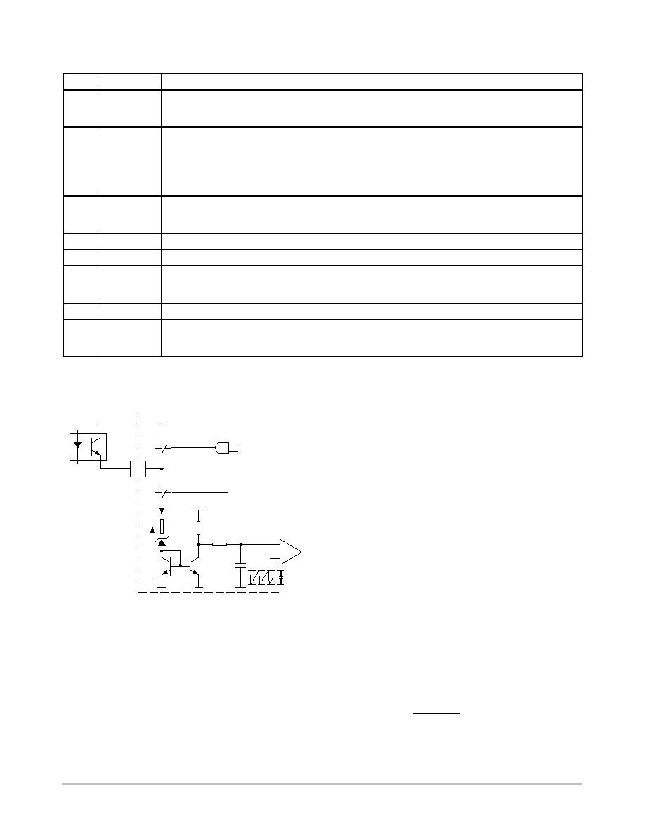
PIN FUNCTION DESCRIPTION
Pin
Name
Description
1
Demag
The Demag pin offers 3 different functions: Zero voltage crossing detection (50mV), 24
╡
A current detection
and 120
╡
A current detection. The 24
╡
A level is used to detect the secondary reconfiguration status and the
120
╡
A level to detect an Over Voltage status called Quick OVP.
2
Isense
The Current Sense pin senses the voltage developed on the series resistor inserted in the source of the
power MOSFET. When Isense reaches 1V, the Driver output (pin 5) is disabled. This is known as the Over
Current Protection function. A 200
╡
A current source is flowing out of the pin 3 during the start¡up phase and
during the switching phase in case of the Pulsed Mode of operation. A resistor can be inserted between the
sense resistor and the pin 3, thus a programmable peak current detection can be performed during the SMPS
stand¡by mode.
3
Control Input
A feedback current from the secondary side of the SMPS via the opto¡coupler is injected into this pin. A
resistor can be connected between this pin and GND to allow the programming of the Burst duty cycle during
the Stand¡by mode.
4
Ground
This pin is the ground of the primary side of the SMPS.
5
Driver
The current and slew rate capability of this pin are suited to drive Power MOSFETs.
6
VCC
This pin is the positive supply of the IC. The driver output gets disabled when the voltage becomes higher
than 15V and the operating range is between 6.6V and 13V. An intermediate voltage level of 10V creates a
disabling condition called Latched Off phase.
7
This pin is to provide isolation between the Vi pin 8 and the VCC pin 6.
8
Vi
This pin can be directly connected to a 500V voltage source for start¡up function of the IC. During the
Start¡up phase a 9 mA current source is internally delivered to the VCC pin 6 allowing a rapid charge of the
VCC capacitor. As soon as the IC starts¡up, this current source is disabled.
OPERATING DESCRIPTION
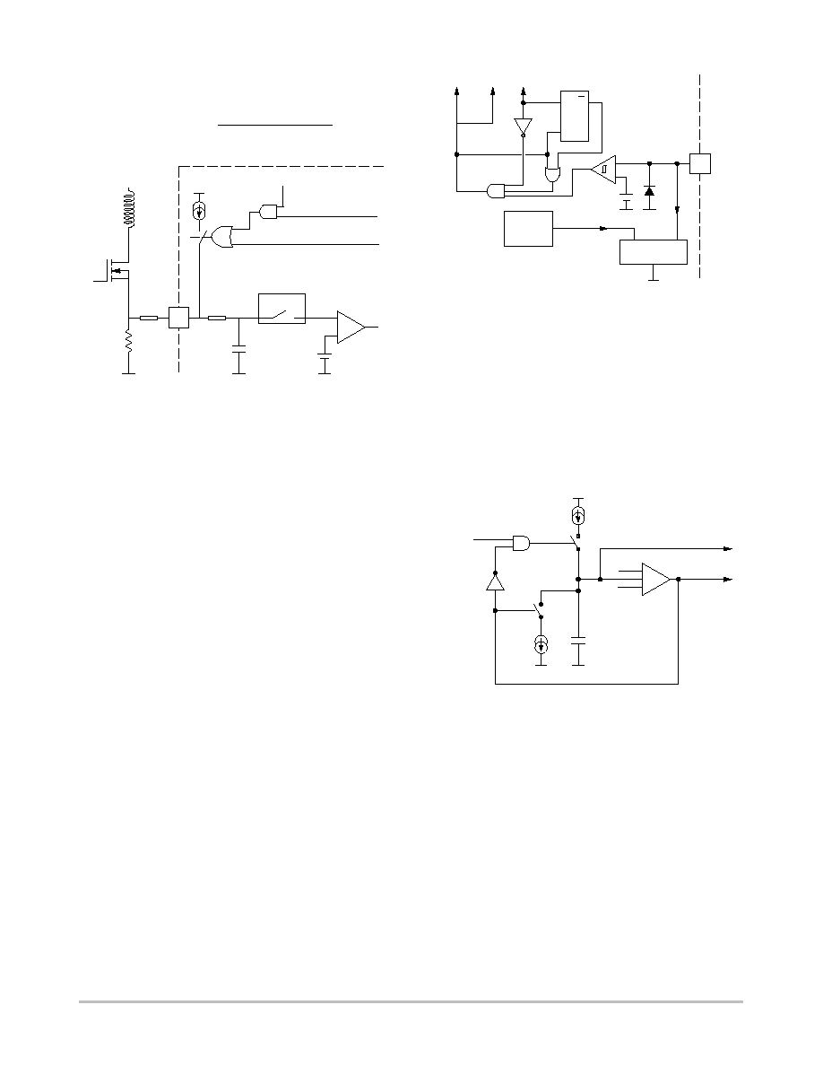
Regulation
Figure 1. Regulator
S3
1
0
&
3
Regulation
20
W
S2
1
0
Control
Input
VCC
V LP¡stby
5 V
4 kHz
Filter
Output
Vdd
PWM
Comparator
Switching Phase
Stand¡by
Latched off Phase
1.6 V
The pin 3 senses the feedback current provided by the opto
coupler. During the switching phase the switch S2 is closed
and the shunt regulator is accessible by the pin 3. The shunt
regulator voltage is typically 5V. The dynamic resistance of
the shunt regulator represented by the zener diode is 20
W.
The gain of the Control input is given on Figure 10 which
shows the duty cycle as a function of the current injected into
the pin 3.
A 4kHz filter network is inserted between the shunt
regulator and the PWM comparator to cancel the high
frequency residual noise.
The switch S3 is closed in Stand¡by mode during the
Latched Off Phase while the switch S2 remains open. (See
section PULSED MODE DUTY CYCLE CONTROL).
The resistor Rdpulsed (Rduty cycle burst) has no effect on
the regulation process. This resistor is used to determine the
burst duty cycle described in the chapter "Pulsed Duty Cycle
Control" on page 8.
PWM Latch
The MC44608 works in voltage mode. The on¡time is
controlled by the PWM comparator that compares the
oscillator sawtooth with the regulation block output (refer to
the block diagram on page 2).
The PWM latch is initialized by the oscillator and is reset
by the PWM comparator or by the current sense comparator
in case of an over current. This configuration ensures that
only a single pulse appears at the circuit output during an
oscillator cycle.
Current Sense
The inductor current is converted to a positive voltage by
inserting a ground reference sense resistor RSense in series
with the power switch.
The maximum current sense threshold is fixed at 1V. The
peak current is given by the following equation:
Ipkmax
+
1
Rsense(
W
)
(A)
MC44608
http://onsemi.com
6
In stand¡by mode, this current can be lowered as due to the
activation of a 200
╡
A current source:
Ipk
max
*
stby
+
1
*
(Rcs(k
W
)
0, 2)
Rsense(
W
)
(A)
Figure 2. Current Sense
+
¡
Switching Phase
1 V
STAND¡BY
1
0
&
2
Isense
L.E.B.
Overcurrent
OC
200 A
m
START¡UP
Comparator
Rcs
Rsense
The current sense input consists of a filter (6k
W, 4pF) and
of a leading edge blanking. Thanks to that, this pin is not
sensitive to the power switch turn on noise and spikes and
practically in most applications, no filtering network is
required to sense the current.
Finally, this pin is used:
¡ as a protection against over currents (Isense > I)
¡ as a reduction of the peak current during a Pulsed Mode
switching phase.
The overcurrent propagation delay is reduced by
producing a sharp output turn off (high slew rate). This
results in an abrupt output turn off in the event of an over
current and in the majority of the pulsed mode switching
sequense.
Demagnetization Section
The MC44608 demagnetization detection consists of a
comparator designed to compare the VCC winding voltage
to a reference that is typically equal to 50mV.
This reference is chosen low to increase effectiveness of
the demagnetization detection even during start¡up.
A latch is incorporated to turn the demagnetization block
output into a low level as soon as a voltage less than 50 mV
is detected, and to keep it in this state until a new pulse is
generated on the output. This avoids any ringing on the input
signal which may alter the demagnetization detection.
For a higher safety, the demagnetization block output is
also directly connected to the output, which is disabled
during the demagnetization phase.
The demagnetization pin is also used for the quick,
programmable OVP. In fact, the demagnetization input
current is sensed so that the circuit output is latched off when
this current is detected as higher than 120
╡
A.
Figure 3. Demagnetization Block
&
1
DMG
> 24 A
Output
Current Mirror
Oscillator Buffer
+
¡
Idemag
Idemag
50/20 mV
>120 A
m
m
Demag
R Q
S
DMG
This function can be inhibited by grounding it but in this
case, the quick and programmable OVP is also disabled.
Oscillator
The MC44608 contains a fixed frequency oscillator. It is
built around a fixed value capacitor CT succesively charged
and discharged by two distinct current sources ICH and
IDCH. The window comparator senses the CT voltage value
and activates the sources when the voltage is reaching the
2.4V/4V levels.
Figure 4. Oscillator Block
+
¡
from Demag
4 V
2.4 V
&
Window
OSC
ICH
comp
DMG
SDCH
IDCH
logic block
SCH
Clock
CT
The complete demagnetization status DMG is used to
inhibit the recharge of the CT capacitor. Thus in case of
incomplete transformer demagnetization the next switching
cycle is postpone until the DMG signal appears. The
oscillator remains at 2.4V corresponding to the sawtooth
valley voltage. In this way the SMPS is working in the so
called SOPS mode (Self Oscillating Power Supply). In that
case the effective switching frequency is variable and no
longer depends on the oscillator timing but on the external
working conditions (Refer to DMG signal in the Figure 5).

MC44608
http://onsemi.com
7
Figure 5.
Vcont
2.4 V
Iprim
DMG
Clock
OSC
4 V
The OSC and Clock signals are provided according to the
Figure 5. The Clock signals correspond to the CT capacitor
discharge. The bottom curve represents the current flowing
in the sense resistor Rcs. It starts from zero and stops when
the sawtooth value is equal to the control voltage Vcont. In
this way the SMPS is regulated with a voltage mode control.
Overvoltage Protection
The MC44608 offers two OVP functions:
¡ a fixed function that detects when VCC is higher than
15.4V
¡ a programmable function that uses the demag pin. The
current flowing into the demag pin is mirrored and
compared to the reference current Iovp (120
╡
A). Thus this
OVP is quicker as it is not impacted by the VCC inertia and
is called QOVP.
In both cases, once an OVP condition is detected, the
output is latched off until a new circuit START¡UP.
Start¡up Management
The Vi pin 8 is directly connected to the HV DC rail Vin.
This high voltage current source is internally connected to
the VCC pin and thus is used to charge the VCC capacitor. The
VCC capacitor charge period corresponds to the Start¡up
phase. When the VCC voltage reaches 13V, the high voltage
9mA current source is disabled and the device starts
working. The device enters into the switching phase.
It is to be noticed that the maximum rating of the Vi pin 8
is 700V. ESD protection circuitry is not currently added to
this pin due to size limitations and technology constraints.
Protection is limited by the drain¡substrate junction in
avalanche breakdown. To help increase the application
safety against high voltage spike on that pin it is possible to
insert a small wattage 1k
W series resistor between the Vin
rail and pin 8.
The Figure 6 shows the VCC voltage evolution in case of
no external current source providing current into the VCC
pin during the switching phase. This case can be
encountered in SMPS when the self supply through an
auxiliary winding is not present (strong overload on the
SMPS output for example). The Figure 16 also depicts this
working configuration.
Figure 6. Hiccup Mode
Start¡up
Latched off
Phase
Switching
Phase
Phase
V
CC
6.5 V
10 V
13 V
In case of the hiccup mode, the duty cycle of the switching
phase is in the range of 10%.
Mode Transition
The LW latch Figure 7 is the memory of the working status
at the end of every switching sequence.
Two different cases must be considered for the logic at the
termination of the SWITCHING PHASE:
1. No Over Current was observed
2. An Over Current was observed
These 2 cases are corresponding to the signal labelled
NOC in case of "No Over Current" and "OC" in case of Over
Current. So the effective working status at the end of the ON
time memorized in LW corresponds to Q=1 for no over
current and Q=0 for over current.
This sequence is repeated during the Switching phase.
Several events can occur:
1. SMPS switch OFF
2. SMPS output overload
3. Transition from Normal to Pulsed Mode
4. Transition from Pulsed Mode to Normal Mode
Figure 7. Transition Logic
&
I
S
Q
R
LW
+
¡
&
CS
Q
&
R2
Q
S
Mode
LEB out
1 V
VPWM
OUT
Stand¡by
R1
Start¡up
Phase
Switching
Phase
Start¡up
Phase
NOC
OC
> 24 A
m
Latched Off
Phase
&
demag
S1
Switch
╖
1. SMPS SWITCH OFF
When the mains is switched OFF, so long as the bulk
electrolithic bulk capacitor provides energy to the SMPS,
the controller remains in the switching phase. Then the peak
current reaches its maximum peak value, the switching
frequency decreases and all the secondary voltages are
reduced. The VCC voltage is also reduced. When VCC is
equal to 10V, the SMPS stops working.

MC44608
http://onsemi.com
8
╖
2. Overload
In the hiccup mode the 3 distinct phases are described as
follows (refer to Figure 6):
The SWITCHING PHASE: The SMPS output is low and
the regulation block reacts by increasing the ON time (dmax
= 80%). The OC is reached at the end of every switching
cycle. The LW latch (Figure 7) is reset before the VPWM
signal appears. The SMPS output voltage is low. The VCC
voltage cannot be maintained at a normal level as the
auxiliary winding provides a voltage which is also reduced
in a ratio similar to the one on the output (i.e. Vout nominal
/ Vout short¡circuit). Consequently the VCC voltage is
reduced at an operating rate given by the combination VCC
capacitor value together with the ICC working consumption
(3.2mA) according to the equation 2. When VCC crosses
10V the WORKING PHASE gets terminated. The LW latch
remains in the reset status.
The LATCHED¡OFF PHASE: The VCC capacitor
voltage continues to drop. When it reaches 6.5V this phase
is terminated. Its duration is governed by equation 3.
The START¡UP PHASE is reinitiated. The high voltage
start¡up current source (¡ICC1 = 9mA) is activated and the
MODE latch is reset. The VCC voltage ramps up according
to the equation 1. When it reaches 13V, the IC enters into the
SWITCHING PHASE.
The NEXT SWITCHING PHASE: The high voltage
current source is inhibited, the MODE latch (Q=0) activates
the NORMAL mode of operation. Figure 2 shows that no
current is injected out pin 2. The over current sense level
corresponds to 1V.
As long as the overload is present, this sequence repeats.
The SWITCHING PHASE duty cycle is in the range of 10%.
╖
3. Transition from Normal to Pulsed Mode
In this sequence the secondary side is reconfigured (refer
to the typical application schematic on page 13). The high
voltage output value becomes lower than the NORMAL
mode regulated value. The TL431 shunt regulator is fully
OFF. In the SMPS stand¡by mode all the SMPS outputs are
lowered except for the low voltage output that supply the
wake¡up circuit located at the isolated side of the power
supply. In that mode the secondary regulation is performed
by the zener diode connected in parallel to the TL431.
The secondary reconfiguration status can be detected on
the SMPS primary side by measuring the voltage level
present on the auxiliary winding Laux. (Refer to the
Demagnetization Section). In the reconfigured status, the
Laux voltage is also reduced. The VCC self¡powering is no
longer possible thus the SMPS enters in a hiccup mode
similar to the one described under the Overload condition.
In the SMPS stand¡by mode the 3 distinct phases are:
The SWITCHING PHASE: Similar to the Overload
mode. The current sense clamping level is reduced
according to the equation of the current sense section, page
5. The C.S. clamping level depends on the power to be
delivered to the load during the SMPS stand¡by mode.
Every switching sequence ON/OFF is terminated by an OC
as long as the secondary Zener diode voltage has not been
reached. When the Zener voltage is reached the ON cycle is
terminated by a true PWM action. The proper SWITCHING
PHASE termination must correspond to a NOC condition.
The LW latch stores this NOC status.
The LATCHED OFF PHASE: The MODE latch is set.
The START¡UP PHASE is similar to the Overload Mode.
The MODE latch remains in its set status (Q=1).
The SWITCHING PHASE: The Stand¡by signal is
validated and the 200
╡
A is sourced out of the Current Sense
pin 2.
╖
4. Transition from Stand¡by to Normal
The secondary reconfiguration is removed. The
regulation on the low voltage secondary rail can no longer
be achieved, thus at the end of the SWITCHING PHASE, no
PWM condition can be encountered. The LW latch is reset.
At the next WORKING PHASE a NORMAL mode status
takes place.
In order to become independent of the recovery time
constant on the secondary side of the SMPS an additional
reset input R2 is provided on the MODE latch. The condition
Idemag<24
╡
A corresponds to the activation of the
secondary reconfiguration status. The R2 reset insures a
return into the NORMAL mode following the first
START¡UP PHASE.
Pulsed Mode Duty Cycle Control
During the sleep mode of the SMPS the switch S3 is
closed and the control input pin 3 is connected to a 4.6V
voltage source thru a 500
W resistor. The discharge rate of the
VCC capacitor is given by ICC¡latch (device consumption
during the LATCHED OFF phase) in addition to the current
drawn out of the pin 3. Connecting a resistor between the Pin
3 and GND (RDPULSED) a programmable current is drawn
from the VCC through pin 3. The duration of the LATCHED
OFF phase is impacted by the presence of the resistor
RDPULSED. The equation 3 shows the relation to the pin 3
current.
Pulsed Mode Phases
Equations 1 through 8 define and predict the effective
behavior during the PULSED MODE operation. The
equations 6, 7, and 8 contain K, Y, and D factors. These
factors are combinations of measured parameters. They
appear in the parameter section "Kfactors for pulsed mode
operation" page 4. In equations 3 through 8 the pin 3 current
is the current defined in the above section "Pulsed Mode
Duty Cycle Control".

MC44608
http://onsemi.com
9
EQUATION 1
Start¡up Phase Duration:
tstart¡up
+
C
Vcc
(Vstup
*
UVLO2)
Istup
where: Istup is the start¡up current flowing through VCC pin
CVcc is the VCC capacitor value
EQUATION 2
Switching Phase Duration:
t
switch
+
C
Vcc
(Vstup
*
UVLO1)
I
ccS
)
I
G
where: IccS is the no load circuit consumption in switching phase
IG is the current consumed by the Power Switch
EQUATION 3
Latched¡off Phase Duration:
t
latched
*
off
+
C
Vcc
(UVLO1
*
UVLO2)
I
ccL
)
I
pin3
where: IccL is the latched off phase consumption
Ipin3 is the current drawn from pin3 adding a resistor
EQUATION 4
Burst Mode Duty Cycle:
d
BM
+
t
switch
tstart
*
up
)
t
switch
)
t
latched
*
off
EQUATION 5
d
BM
+
C
Vcc
(V
stup
*
UVLO1)
I
ccS
)
I
G
C
Vcc
(V
stup
*
UVLO2)
I
stup
)
C
Vcc
(V
stup
*
UVLO1)
I
ccS
)
I
G
)
C
Vcc
(UVLO1
*
UVLO2)
I
ccL
)
I
pin3
EQUATION 6
d
BM
+
1
1
)
k
S Stup
I
ccS
)
I
G
I
stup
)
k
S L
I
ccS
)
I
G
I
ccL
)
I
pin3
where: kS/Stup = (Vstup ¡ UVLO2)/(Vstup ¡ UVLO1)
kS/L = (UVLO1 ¡ UVLO2)/(Vstup ¡ UVLO1)

MC44608
http://onsemi.com
10
EQUATION 7
d
BM
+
1
1
)
I
ccS
)
I
G
I
stup
k
S Stup
)
k
S L
I
stup
I
ccL
)
I
pin3
EQUATION 8
d
BM
+
1
1
)
k1
)
I
G
I
stup
k
S Stup
)
(k
S L
1
k2
)
I
pin3
I
stup
)
where: k1 = Iccs/Istup
k2 = IccL/Istup
kS/Stup = (Vstup¡UVLO2)/(Vstup¡UVLO1)
kS/L = (UVLO1¡UVLO2)/(Vstup¡UVLO1)
PULSED MODE CURRENT SENSE CLAMPING LEVEL
Equations 9, 10, 11 and 12 allow the calculation of the Rcs value for the desired maximum current peak value during the
SMPS stand¡by mode.
EQUATION 9
Ipk
stby
+
V
cs¡th
*
(Rcs
Ics)
R
S
where: Vcs¡th is the CS comparator threshold
Ics is the CS internal current source
RS is the sensing resistor
Rcs is the resistor connected between pin 2 and RS
EQUATION 10
Ipk
stby
+
V
cs¡th
1
*
Rcs
Ics
V
cs¡th
R
S
EQUATION 11
Ipk
stby
+
V
cs¡th
1
*
(Rcs
Y
cs¡stby
)
R
S
where: Ycs¡stby = Ics/Vcs¡th
Taking into account the circuit propagation delay (
d
tcs) and the Power Switch reaction time (
d
tps):
EQUATION 12
Ipk
stby
+
V
cs¡th
1
*
(Rcs
Y
cs¡stby
)
R
S
)
V
in
(
d
tcs
) d
tps)
Lp
MC44608
http://onsemi.com
11
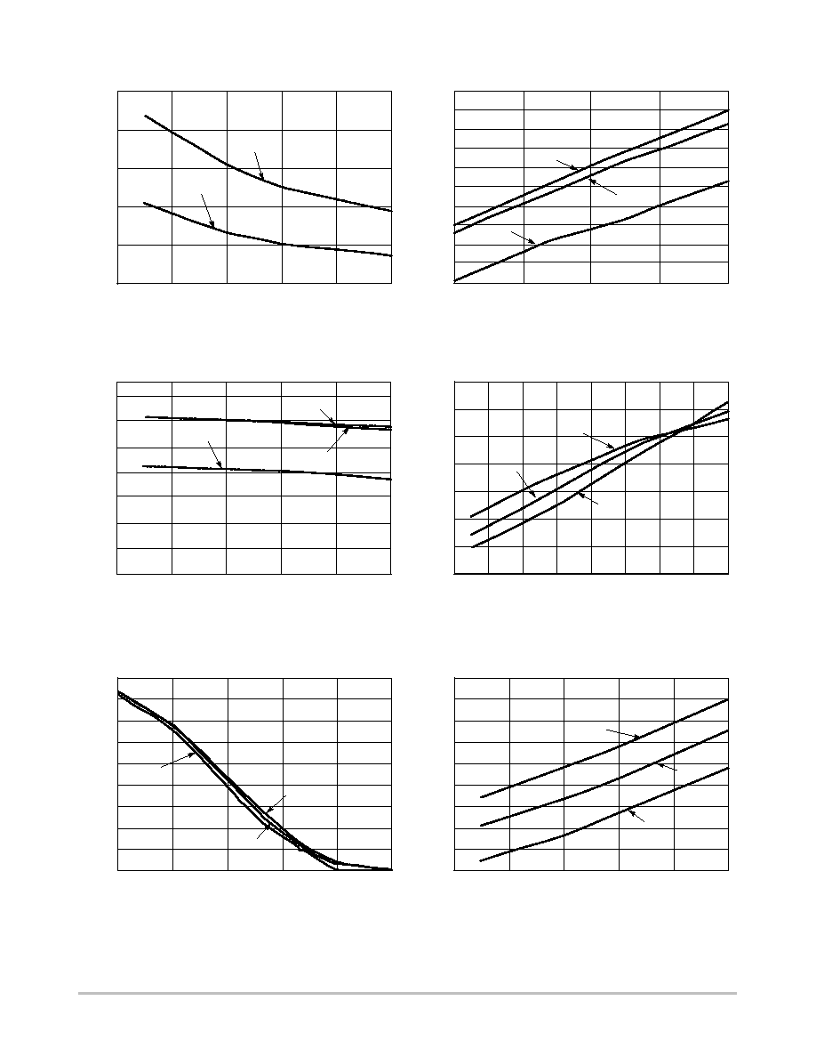
1.5
Vpin3 V
oltage
(V)
¡1.6
Current Injected in Pin 3 (mA)
¡25
░
C
25
░
C
85
░
C
¡1.4
¡1.2
¡1.0
¡.08
¡.06
¡.04
¡.02
0.0
2.0
2.5
3.0
3.5
4.0
4.5
5.0
Figure 8. Output Switching Speed
10
T
ime (nS)
20
30
40
50
60
10
11
12
13
14
15
t_fall
t_rise
Pin6 VCC Voltage (V)
4.98
Vpin3 (V)
0.5
1.5
2
2.5
Current Injected in Pin 3 (mA)
1
4.99
5.00
5.01
5.02
5.03
5.04
5.05
5.06
5.07
5.08
¡25
░
C
25
░
C
85
░
C
Figure 9. Frequency Stability
Figure 10. Duty Cycle Control
65.0
Fr
eq
u
ency
67.0
71.0
75.0
77.0
79.0
10
11
12
13
14
15
VCC Voltage (V)
Figure 11. Vpin3 During the Working Period
Figure 12. Vpin3 During the Latched Off Period
Figure 13. Device Consumption when Switching
73.0
69.0
¡25
░
C
25
░
C
85
░
C
0
Switching Duty Cycle (%)
10
40
60
70
80
0.0
0.5
1.0
1.5
2.0
2.5
Current Injected in Pin3 (mA)
50
20
¡25
░
C
25
░
C
85
░
C
90
30
3.00
Pin6 Current (mA)
3.20
3.80
4.20
4.40
4.60
10
11
12
13
14
15
Pin6 VCC Voltage (V)
4.00
3.40
¡25
░
C
25
░
C
85
░
C
4.80
3.60
MC44608
http://onsemi.com
12
5.00
¡Icc (mA)
6.00
7.00
8.00
10.00
11.00
0
100
200
300
400
500
Vi Pin8 Voltage (Vi)
¡25
░
C
25
░
C
85
░
C
9.00
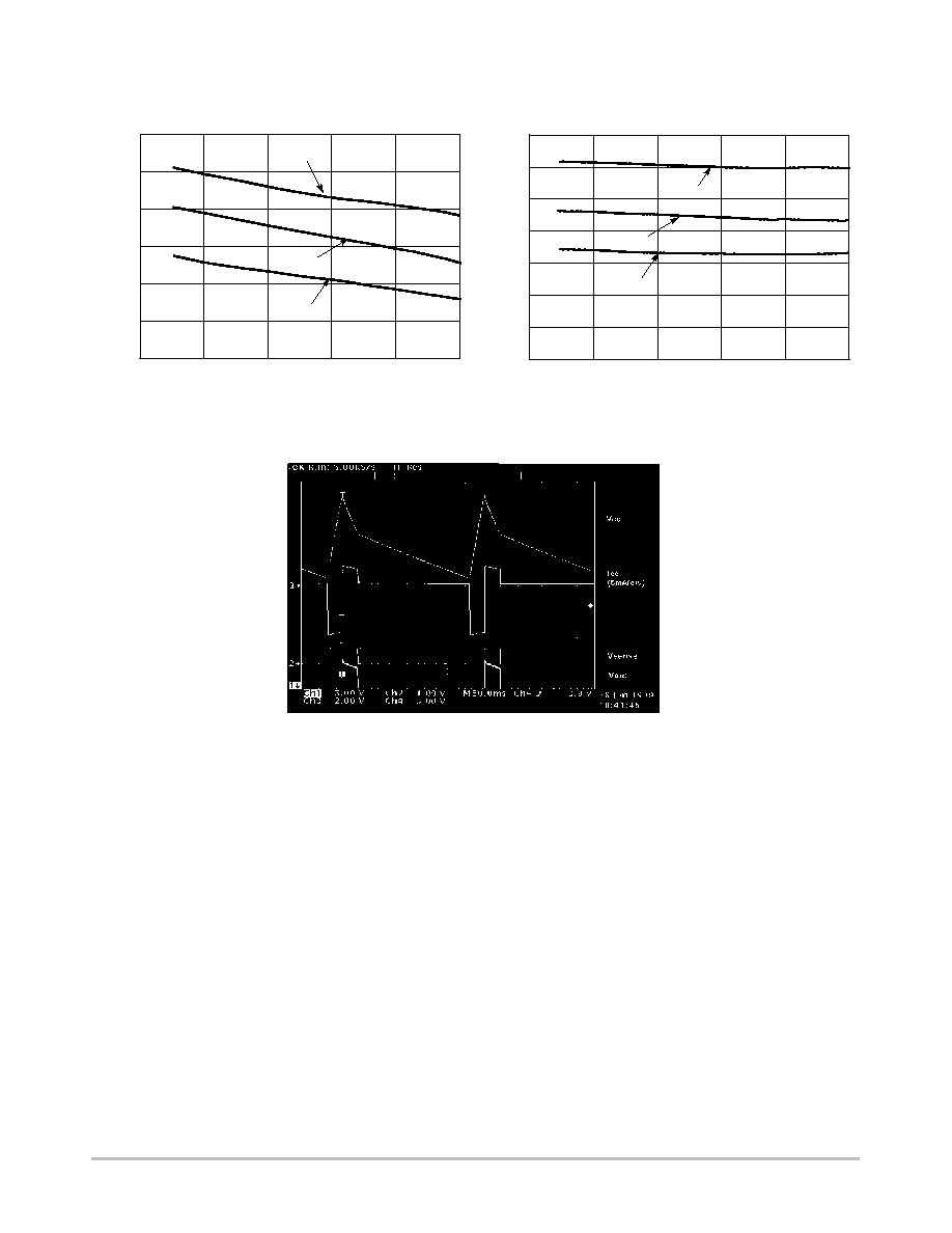
Figure 14. High Voltage Current Source
5.00
Switching Duty Cycle (%)
6.00
7.00
8.00
11.00
0
100
200
300
400
500
Vi Pin Voltage (V)
¡25
░
C
25
░
C
85
░
C
9.00
Figure 15. Overload Burst Mode
10.00
12.00
Figure 16. Hiccup Mode Waveforms
The data in Figure 15 corresponds to the waveform in
Figure 16. The Figure 16 shows VCC, ICC, Isense (pin 2) and
Vout (pin 5). Vout (pin 5) in fact shows the envelope of the
output switching pulses. This mode corresponds to an
overload condition.
MC44608
http://onsemi.com
13
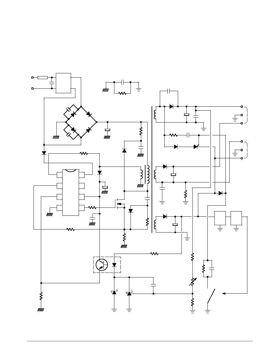
The Figure 18 represents a complete power supply using the secondary reconfiguration.
The specification is as follows:
Input source:
85Vac to 265Vac
3 Outputs
112V / 0.45A
16V / 1.5A
8V / 1A
Output power
80W
Stand¡by mode
@ Pout = 300mW, 1.3W
Figure 17. Typical Application
+
+
+
+
22 F
m
+
I
8
7
6
5
1
2
3
4
RFI
FILTER
2N2FY
4.7 k
W
47 k
1N4934
120 pF
MC44608P75
R10
W
10 k
R9
W
100 k
R8
W
2.4 k
R12
W
1 k
C18
100 nF
m
C19
33 nF
R11
4.7 k
W
MTP6N60E
D7
1N4148
R5
100 k
W
C7
16 V
VCC
R21
47
W
R3
0.27
W
OPT1
C8
100 nF
R4
3.9 k
W
D13
1N4148
Post
Reg.
P
OFF
ON
ON = Normal Mode
OFF = Pulsed Mode
D14
MR856
R17
W
2.2 k
5 W
C9
470 pF
630 V
8
9
R19
W
18 k
11
10
14
12
C16
120 pF
D10
MR852
C14
1000
mF
35 V
D9
MR852
C15
F
1000
m
16 V
3
2
1
3
2
1
C17
D12
R7
W
C12
F
47
m
250 V
C13
100 nF
D18
MR856
220 pF
500 V
C11
C20
C3
1 nF
C4
1 nF
D1, D2, D3, D4
1N5404
R1
W
22 k
5 W
C5
220
mF
400 V
C6
47 nF
630 V
D6
MR856
sense
6
7
1
2
FI
C1
100 nF
WIDE
AINS
47288900
R F6
D5
1N4007
J4
J3
8 V/1 A
16 V/1.5 A
112 V/0.45 A
4 kV
R16
MCR22¡6
DZ1
DZ3
10 V
DZ2
TL431CLP
R2
W
10

MC44608
http://onsemi.com
14
The secondary reconfiguration is activated by the
╡
P
through the switch. The dV/dt appearing on the high voltage
winding (pins 14 of the transformer) at every TMOS switch
off, produces a current spike through the series RC network
R7, C17. According to the switch position this spike is either
absorbed by the ground (switch closed) or flows into the
thyristor gate (switch open) thus firing the MCR22¡6. The
closed position of the switch corresponds to the Pulsed
Mode activation. In this secondary side SMPS status the
high voltage winding (12¡14) is connected through D12 and
DZ1 to the 8V low voltage secondary rail. The voltages
applied to the secondary windings 12¡14, 10¡11 and 6¡7
(Vaux) are thus divided by ratio N12¡14 / N9¡8 (number of
turns of the winding 12¡14 over number of turns of the
winding 9¡8). In this reconfigured status all the secondary
voltages are lowered except the 8V one. The regulation
during every pulsed or burst is performed by the zener diode
DZ3 which value has to be choosen higher than the normal
mode regulation level. This working mode creates a voltage
ripple on the 8V rail which generally must be post regulated
for the microProcessor supply.
Figure 18. SMPS Pulsed Mode
The Figure 18 shows the SMPS behavior while working
in the reconfigured mode. The top curve represents the VCC
voltage (pin 6 of the MC44608). The middle curve
represents the 8V rail. The regulation is taking place at
11.68V. On the bottom curve the pin 2 voltage is shown. This
voltage represents the current sense signal. The pin 2 voltage
is the result of the 200
╡
A current source activated during the
start¡up phase and also during the working phase which
flows through the R4 resistor. The used high resolution
mode of the oscilloscope does not allow to show the
effective ton current flowing in the sensing resistor R11.
MC44608
http://onsemi.com
15
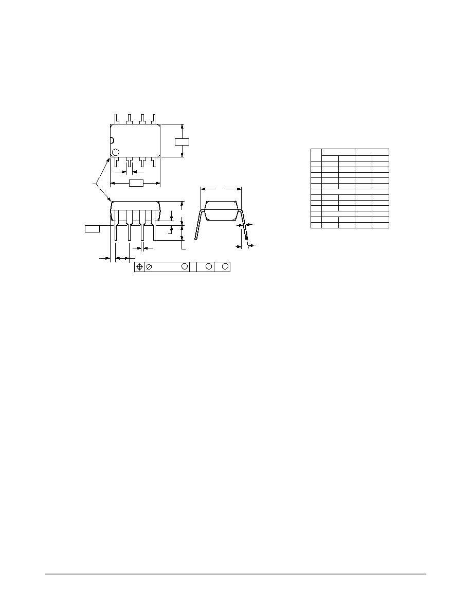
PACKAGE DIMENSIONS
DIP¡8
P SUFFIX
PLASTIC PACKAGE
CASE 626¡05
ISSUE K
NOTES:
1. DIMENSION L TO CENTER OF LEAD WHEN
FORMED PARALLEL.
2. PACKAGE CONTOUR OPTIONAL (ROUND OR
SQUARE CORNERS).
3. DIMENSIONING AND TOLERANCING PER ANSI
Y14.5M, 1982.
STYLE 1:
PIN 1. AC IN
2. DC + IN
3. DC ¡ IN
4. AC IN
5. GROUND
6. OUTPUT
7. AUXILIARY
8. VCC
1
4
5
8
F
NOTE 2
¡A¡
¡B¡
¡T¡
SEATING
PLANE
H
J
G
D
K
N
C
L
M
M
A
M
0.13 (0.005)
B
M
T
DIM
MIN
MAX
MIN
MAX
INCHES
MILLIMETERS
A
9.40
10.16
0.370
0.400
B
6.10
6.60
0.240
0.260
C
3.94
4.45
0.155
0.175
D
0.38
0.51
0.015
0.020
F
1.02
1.78
0.040
0.070
G
2.54 BSC
0.100 BSC
H
0.76
1.27
0.030
0.050
J
0.20
0.30
0.008
0.012
K
2.92
3.43
0.115
0.135
L
7.62 BSC
0.300 BSC
M
¡¡¡
10
¡¡¡
10
N
0.76
1.01
0.030
0.040
_
_

MC44608
http://onsemi.com
16
ON Semiconductor and are trademarks of Semiconductor Components Industries, LLC (SCILLC). SCILLC reserves the right to make changes
without further notice to any products herein. SCILLC makes no warranty, representation or guarantee regarding the suitability of its products for any particular
purpose, nor does SCILLC assume any liability arising out of the application or use of any product or circuit, and specifically disclaims any and all liability,
including without limitation special, consequential or incidental damages. "Typical" parameters which may be provided in SCILLC data sheets and/or
specifications can and do vary in different applications and actual performance may vary over time. All operating parameters, including "Typicals" must be
validated for each customer application by customer's technical experts. SCILLC does not convey any license under its patent rights nor the rights of others.
SCILLC products are not designed, intended, or authorized for use as components in systems intended for surgical implant into the body, or other applications
intended to support or sustain life, or for any other application in which the failure of the SCILLC product could create a situation where personal injury or
death may occur. Should Buyer purchase or use SCILLC products for any such unintended or unauthorized application, Buyer shall indemnify and hold
SCILLC and its officers, employees, subsidiaries, affiliates, and distributors harmless against all claims, costs, damages, and expenses, and reasonable
attorney fees arising out of, directly or indirectly, any claim of personal injury or death associated with such unintended or unauthorized use, even if such claim
alleges that SCILLC was negligent regarding the design or manufacture of the part. SCILLC is an Equal Opportunity/Affirmative Action Employer.
PUBLICATION ORDERING INFORMATION
CENTRAL/SOUTH AMERICA:
Spanish Phone: 303¡308¡7143 (Mon¡Fri 8:00am to 5:00pm MST)
Email: ONlit¡spanish@hibbertco.com
ASIA/PACIFIC: LDC for ON Semiconductor ¡ Asia Support
Phone: 303¡675¡2121 (Tue¡Fri 9:00am to 1:00pm, Hong Kong Time)
Toll Free from Hong Kong & Singapore:
001¡800¡4422¡3781
Email: ONlit¡asia@hibbertco.com
JAPAN: ON Semiconductor, Japan Customer Focus Center
4¡32¡1 Nishi¡Gotanda, Shinagawa¡ku, Tokyo, Japan 141¡8549
Phone: 81¡3¡5740¡2745
Email: r14525@onsemi.com
ON Semiconductor Website: http://onsemi.com
For additional information, please contact your local
Sales Representative.
MC44608/D
NORTH AMERICA Literature Fulfillment:
Literature Distribution Center for ON Semiconductor
P.O. Box 5163, Denver, Colorado 80217 USA
Phone: 303¡675¡2175 or 800¡344¡3860 Toll Free USA/Canada
Fax: 303¡675¡2176 or 800¡344¡3867 Toll Free USA/Canada
Email: ONlit@hibbertco.com
Fax Response Line: 303¡675¡2167 or 800¡344¡3810 Toll Free USA/Canada
N. American Technical Support: 800¡282¡9855 Toll Free USA/Canada
EUROPE: LDC for ON Semiconductor ¡ European Support
German Phone: (+1) 303¡308¡7140 (M¡F 1:00pm to 5:00pm Munich Time)
Email: ONlit¡german@hibbertco.com
French Phone: (+1) 303¡308¡7141 (M¡F 1:00pm to 5:00pm Toulouse Time)
Email: ONlit¡french@hibbertco.com
English Phone: (+1) 303¡308¡7142 (M¡F 12:00pm to 5:00pm UK Time)
Email: ONlit@hibbertco.com
EUROPEAN TOLL¡FREE ACCESS*: 00¡800¡4422¡3781
*Available from Germany, France, Italy, England, Ireland