Äîêóìåíòàöèÿ è îïèñàíèÿ www.docs.chipfind.ru
©
Semiconductor Components Industries, LLC, 2005
January, 2005 - Rev. 1
1
Publication Order Number:
74FST3244/D
74FST3244
8-Bit Bus Switch
The ON Semiconductor 74FST3244 is an 8-bit, high performance
switch. The device is CMOS TTL compatible when operating between
4 and 5.5 Volts. The device exhibits extremely low R
ON
and adds
nearly zero propagation delay. The device adds no noise or ground
bounce to the system.
The device consists of two 4-bit switches with separate
Output/Enable (OE) pins. Port A is connected to Port B when OE is
low. If OE is high, the switch is high Z.
Features
·
R
ON
t 4 W Typical
·
Less Than 0.25 ns-Max Delay Through Switch
·
Nearly Zero Standby Current
·
No Circuit Bounce
·
Control Inputs are TTL/CMOS Compatible
·
Pin-For-Pin Compatible with QS3244, FST3244, CBT3244
·
All Popular Packages: QSOP-20, TSSOP-20, SOIC-20
·
All Devices in Package TSSOP are Inherently Pb-Free*
OE
1
1A
1
2B
1
1A
2
2B
2
2B
3
1A
0
V
CC
2A
3
1B
2
2A
2
1B
1
1B
0
OE
2
1
2
3
4
5
6
7
20
19
18
17
16
15
14
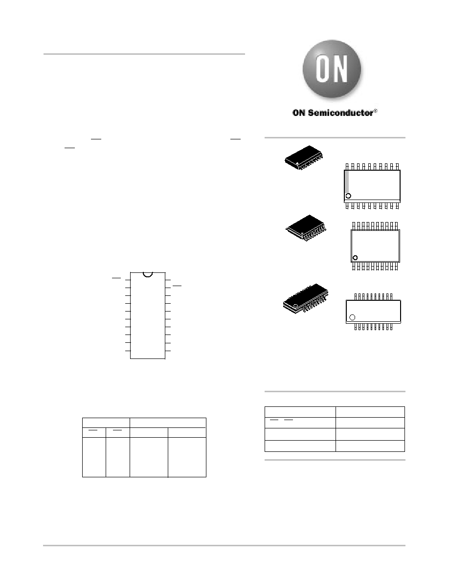
Figure 1. 20-Lead Pinout
1A
3
8
2B
0
9
GND
10
2A
1
13
1B
3
12
2A
0
11
OE
1
L
Inputs
L
H
OE
2
L
H
L
H
H
1A, 1B
1A = 1B
1A = 1B
Inputs/Outputs
Z
Z
2A, 2B
2A = 2B
Z
2A = 2B
Z
TRUTH TABLE
*For additional information on our Pb-Free strategy and soldering details, please
download the ON Semiconductor Soldering and Mounting Techniques
Reference Manual, SOLDERRM/D.
Description
PIN NAMES
OE
1
, OE
2
1A, 2A
TSSOP-20
DT SUFFIX
CASE 948E
QSOP-20
QS SUFFIX
CASE 492A
SOIC-20
DW SUFFIX
CASE 751D
MARKING
DIAGRAMS
Pin
Bus Switch Enables
Bus A
1B, 2B
Bus B
20
1
FST3244
AWLYYWW
1
20
20
1
FST
3244
ALYW
A
= Assembly Location
L, WL
= Wafer Lot
Y
= Year
W, WW = Work Week
1
20
FST3244
AWLYWW
20
1
See detailed ordering and shipping information in the package
dimensions section on page 2 of this data sheet.
ORDERING INFORMATION
20
1
http://onsemi.com
74FST3244
http://onsemi.com
2
2
1
5
9
10
12
3
6
8
11
OE
1
OE
3
Figure 2. Logic Diagram
1A
0
1A
3
2A
0
2A
3
1B
0
1B
3
2B
0
2B
3
ORDERING INFORMATION
Device Order N mber
Package
Shipping
Device Order Number
Package
Shipping
74FST3244DW
SOIC-20
55 Units / Rail
74FST3244DWR2
SOIC-20
1000 Units / Tape & Reel
74FST3244DT
TSSOP-20*
(Pb-Free)
75 Units / Rail
74FST3244DTR2
TSSOP-20*
(Pb-Free)
2500 Units / Tape & Reel
74FST3244QS
QSOP-20
55 Units / Rail
74FST3244QSR
QSOP-20
2500 Units / Tape & Reel
For information on tape and reel specifications, including part orientation and tape sizes, please refer to our Tape and Reel Packaging
Specifications Brochure, BRD8011/D.
*This package is inherently Pb-Free.
74FST3244
http://onsemi.com
3
MAXIMUM RATINGS
Symbol
Parameter
Value
Unit
V
CC
DC Supply Voltage
*
0.5 to
)
7.0
V
V
I
DC Input Voltage
*
0.5 to
)
7.0
V
V
O
DC Output Voltage
*
0.5 to
)
7.0
V
I
IK
DC Input Diode Current
V
I
t
GND
*
50
mA
I
OK
DC Output Diode Current
V
O
t
GND
*
50
mA
I
O
DC Output Sink Current
128
mA
I
CC
DC Supply Current per Supply Pin
$
100
mA
I
GND
DC Ground Current per Ground Pin
$
100
mA
T
STG
Storage Temperature Range
*
65 to
)
150
_
C
T
L
Lead Temperature, 1 mm from Case for 10 Seconds
260
_
C
T
J
Junction Temperature Under Bias
)
150
_
C
q
JA
Thermal Resistance (Note 1)
SOIC
TSSOP
QSOP
96
128
200
_
C/W
MSL
Moisture Sensitivity
Level 1
F
R
Flammability Rating
Oxygen Index: 28 to 34
UL 94 V-0 @ 0.125 in
V
ESD
ESD Withstand Voltage
Human Body Model (Note 2)
Machine Model (Note 3)
u
2000
u
200
V
I
Latchup
Latchup Performance
Above V
CC
and Below GND at 85
_
C (Note 4)
$
500
mA
Maximum ratings are those values beyond which device damage can occur. Maximum ratings applied to the device are individual stress limit
values (not normal operating conditions) and are not valid simultaneously. If these limits are exceeded, device functional operation is not implied,
damage may occur and reliability may be affected.
1. Measured with minimum pad spacing on an FR4 board, using 10 mm-by-1 inch, 2-ounce copper trace with no air flow.
2. Tested to EIA/JESD22-A114-A.
3. Tested to EIA/JESD22-A115-A.
4. Tested to EIA/JESD78.
RECOMMENDED OPERATING CONDITIONS
Symbol
Parameter
Min
Max
Unit
V
CC
Supply Voltage
Operating, Data Retention Only
4.0
5.5
V
V
I
Input Voltage
(Note )
0
5.5
V
V
O
Output Voltage
(HIGH or LOW State)
0
V
CC
V
T
A
Operating Free-Air Temperature
*
40
)
85
_
C
D
t/
D
V
Input Transition Rise or Fall Rate
Switch Control Input
Switch I/O
0
0
5
DC
ns/V
5. Unused control inputs may not be left open. All control inputs must be tied to a high or low logic input voltage level.
74FST3244
http://onsemi.com
4
DC ELECTRICAL CHARACTERISTICS
V
CC
T
A
=
*
40
_
C to
)
85
_
C
Symbol
Parameter
Conditions
(V)
Min
Typ*
Max
Unit
V
IK
Clamp Diode Resistance
I
IN
=
*
18mA
4.5
*
1.2
V
V
IH
High-Level Input Voltage
4.0 to 5.5
2.0
V
V
IL
Low-Level Input Voltage
4.0 to 5.5
0.8
V
I
I
Input Leakage Current
0
v
V
IN
v
5.5 V
5.5
$
1.0
m
A
I
OZ
OFF-STATE Leakage Current
0
v
A, B
v
V
CC
5.5
$
1.0
m
A
R
ON
Switch On Resistance (Note 6)
V
IN
= 0 V, I
IN
= 64 mA
4.5
4
7
W
V
IN
= 0 V, I
IN
= 30 mA
4.5
4
7
V
IN
= 2.4 V, I
IN
= 15 mA
4.5
8
15
V
IN
= 2.4 V, I
IN
= 15 mA
4.0
11
20
I
CC
Quiescent Supply Current
V
IN
= V
CC
or GND, I
OUT
= 0
5.5
3
m
A
D
I
CC
Increase In I
CC
per Input
One input at 3.4 V, Other inputs at V
CC
or GND
5.5
2.5
mA
*Typical values are at V
CC
= 5.0 V and T
A
= 25
_
C.
6. Measured by the voltage drop between A and B pins at the indicated current through the switch. On resistance is determined by the lower
of the voltages on the two (A or B) pins.
AC ELECTRICAL CHARACTERISTICS
Limits
T
A
=
*
40
_
C to
)
85
_
C
V
CC
= 4.5 to 5.5 V
V
CC
= 4.0 V
Symbol
Parameter
Conditions
Figures
Min
Max
Min
Max
Unit
t
PHL
,
t
PLH
Prop Delay Bus to Bus
(Note 7)
V
I
= OPEN
3 and 4
0.25
0.25
ns
t
PZH
,
t
PZL
Output Enable Time
V
I
= 7 V for t
PZL
V
I
= OPEN for t
PZH
3 and 4
1.0
5.6
6.1
ns
t
PHZ
,
t
PLZ
Output Disable Time
V
I
= 7 V for t
PLZ
V
I
= OPEN for t
PHZ
3 and 4
1.5
6.2
5.6
ns
7. This parameter is guaranteed by design but is not tested. The bus switch contributes no propagation delay other than the RC delay of the
typical On resistance of the switch and the 50 pF load capacitance, when driven by an ideal voltage source (zero output impedance).
CAPACITANCE (Note 8)
Symbol
Parameter
Conditions
Typ
Max
Unit
C
IN
Control Pin Input Capacitance
V
CC
= 5.0 V
3
pF
C
I/O
Input/Output Capacitance
V
CC
, OE = 5.0 V
5
pF
8. T
A
=
)
25
_
C, f = 1 MHz, Capacitance is characterized but not tested.
74FST3244
http://onsemi.com
5
V
I
V
OL
V
OL
+ 0.3 V
t
PLH
t
PLH
V
OL
V
OH
V
OH
- 0.3 V
t
PHZL
t
f
= 2.5 nS
90 %
1.5 V
10 %
10 %
1.5 V
90 %
t
f
= 2.5 nS
t
PZL
t
PZL
OUTPUT
1.5 V
OUTPUT
1.5 V
GND
3.0 V
t
PZH
ENABLE
INPUT
t
f
= 2.5 nS
90 %
1.5 V
1.5 V
90 %
10 %
10 %
1.5 V
1.5 V
V
OH
GND
3.0 V
SWITCH
INPUT
t
f
= 2.5 nS
C
L
*
FROM
OUTPUT
UNDER
TEST
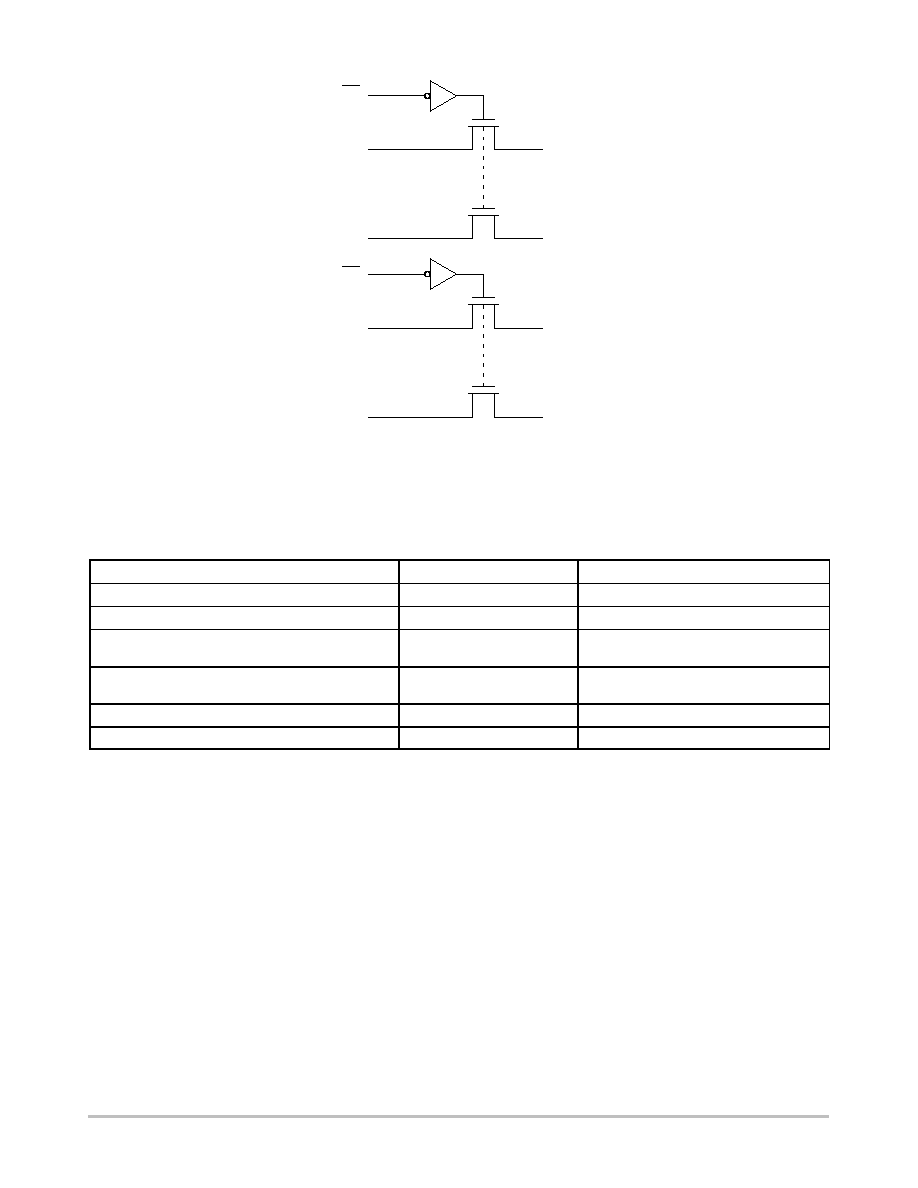
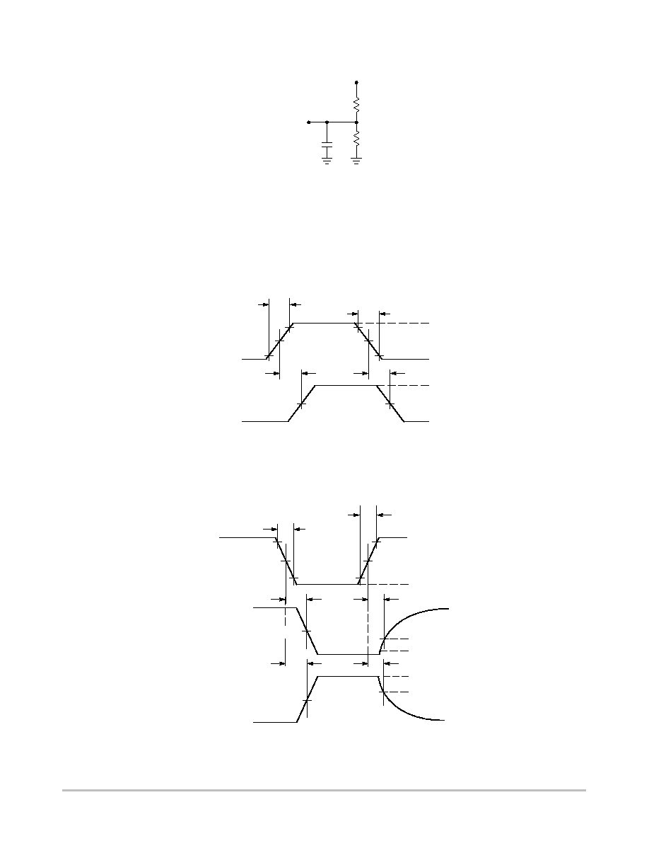
Figure 3. AC Test Circuit
Figure 4. Propagation Delays
AC Loading and Waveforms
NOTES:
1. Input driven by 50
W
source terminated in 50
W
.
2. CL includes load and stray capacitance.
*C
L
= 50 pF
500
W
500
W
Figure 5. Enable/Disable Delays
OUTPUT
74FST3244
http://onsemi.com
6
PACKAGE DIMENSIONS
SOIC-20
DW SUFFIX
CASE 751D-05
ISSUE G
20
1
11
10
B
20X
H
10X
C
L
18X
A1
A
SEATING
PLANE
q
h
X 45
_
E
D
M
0.25
M
B
M
0.25
S
A
S
B
T
e
T
B
A
DIM
MIN
MAX
MILLIMETERS
A
2.35
2.65
A1
0.10
0.25
B
0.35
0.49
C
0.23
0.32
D
12.65
12.95
E
7.40
7.60
e
1.27 BSC
H
10.05
10.55
h
0.25
0.75
L
0.50
0.90
q
0
7
NOTES:
1. DIMENSIONS ARE IN MILLIMETERS.
2. INTERPRET DIMENSIONS AND TOLERANCES
PER ASME Y14.5M, 1994.
3. DIMENSIONS D AND E DO NOT INCLUDE MOLD
PROTRUSION.
4. MAXIMUM MOLD PROTRUSION 0.15 PER SIDE.
5. DIMENSION B DOES NOT INCLUDE DAMBAR
PROTRUSION. ALLOWABLE PROTRUSION
SHALL BE 0.13 TOTAL IN EXCESS OF B
DIMENSION AT MAXIMUM MATERIAL
CONDITION.
_
_
TSSOP-20
DT SUFFIX
CASE 948E-02
ISSUE B
DIM
A
MIN
MAX
MIN
MAX
INCHES
6.60
0.260
MILLIMETERS
B
4.30
4.50
0.169
0.177
C
1.20
0.047
D
0.05
0.15
0.002
0.006
F
0.50
0.75
0.020
0.030
G
0.65 BSC
0.026 BSC
H
0.27
0.37
0.011
0.015
J
0.09
0.20
0.004
0.008
J1
0.09
0.16
0.004
0.006
K
0.19
0.30
0.007
0.012
K1
0.19
0.25
0.007
0.010
L
6.40 BSC
0.252 BSC
M
0 8 0 8
_
_
_
_
NOTES:
1. DIMENSIONING AND TOLERANCING
PER ANSI Y14.5M, 1982.
2. CONTROLLING DIMENSION:
MILLIMETER.
3. DIMENSION A DOES NOT INCLUDE
MOLD FLASH, PROTRUSIONS OR GATE
BURRS. MOLD FLASH OR GATE BURRS
SHALL NOT EXCEED 0.15 (0.006) PER
SIDE.
4. DIMENSION B DOES NOT INCLUDE
INTERLEAD FLASH OR PROTRUSION.
INTERLEAD FLASH OR PROTRUSION
SHALL NOT EXCEED 0.25 (0.010) PER
SIDE.
5. DIMENSION K DOES NOT INCLUDE
DAMBAR PROTRUSION. ALLOWABLE
DAMBAR PROTRUSION SHALL BE 0.08
(0.003) TOTAL IN EXCESS OF THE K
DIMENSION AT MAXIMUM MATERIAL
CONDITION.
6. TERMINAL NUMBERS ARE SHOWN
FOR REFERENCE ONLY.
7. DIMENSION A AND B ARE TO BE
DETERMINED AT DATUM PLANE -W-.
ÍÍÍÍ
ÍÍÍÍ
ÍÍÍÍ
1
10
11
20
PIN 1
IDENT
A
B
-T-
0.100 (0.004)
C
D
G
H
SECTION N-N
K
K1
J J1
N
N
M
F
-W-
SEATING
PLANE
-V-
-U-
S
U
M
0.10 (0.004)
V
S
T
20X REF
K
L
L/2
2X
S
U
0.15 (0.006) T
DETAIL E
0.25 (0.010)
DETAIL E
6.40
0.252
---
---
S
U
0.15 (0.006) T
74FST3244
http://onsemi.com
7
PACKAGE DIMENSIONS
QSOP-20
QS SUFFIX
CASE 492A-01
ISSUE O
MIN
MILLIMETERS
G
R
-B-
-A-
L
M
0.25 (0.010)
T
U
-T-
SEATING
PLANE
K
D
20 PL
C
M
0.25 (0.010)
T B
A
S
S
V
N
M
F
8 PL
DETAIL E
DETAIL E
H x 45
_
RAD.
MOLD PIN
DIM
MAX
MIN
MAX
INCHES
A
8.56
8.74
0.337
0.344
B
3.81
3.99
0.150
0.157
C
1.55
1.73
0.061
0.068
D
0.20
0.31
0.008
0.012
F
0.41
0.89
0.016
0.035
G
0.64 BSC
0.025 BSC
H
0.20
0.46
0.008
0.018
J
0.249
0.191
0.0098 0.0075
K
0.10
0.25
0.004
0.010
L
5.84
6.20
0.230
0.244
M
0
8
0
8
N
0
7
0
7
P
1.32
1.58
0.052
0.062
Q
0.89 DIA
0.035 DIA
R
0.89
1.14
0.035
0.045
U
0.89
1.14
0.035
0.045
V
NOTES:
1. DIMENSIONING AND TOLERANCING PER ANSI
Y14.5M, 1982.
2. CONTROLLING DIMENSION: INCH.
3. THE BOTTOM PACKAGE SHALL BE BIGGER THAN
THE TOP PACKAGE BY 4 MILS (NOTE: LEAD SIDE
ONLY). BOTTOM PACKAGE DIMENSION SHALL
FOLLOW THE DIMENSION STATED IN THIS
DRAWING.
4. PLASTIC DIMENSIONS DOES NOT INCLUDE MOLD
FLASH OR PROTRUSIONS. MOLD FLASH OR
PROTRUSIONS SHALL NOT EXCEED 6 MILS PER
SIDE.
5. BOTTOM EJECTOR PIN WILL INCLUDE THE
COUNTRY OF ORIGIN (COO) AND MOLD CAVITY I.D.
_
_
_
_
0
8
0
_
_
_
8
_
_
_
_
_
MARK
Q
P
0.013 X 0.005
DP. MAX
RAD.
0.005-0.010
TYP
J
74FST3244
http://onsemi.com
8
ON Semiconductor and are registered trademarks of Semiconductor Components Industries, LLC (SCILLC). SCILLC reserves the right to make changes without further notice
to any products herein. SCILLC makes no warranty, representation or guarantee regarding the suitability of its products for any particular purpose, nor does SCILLC assume any liability
arising out of the application or use of any product or circuit, and specifically disclaims any and all liability, including without limitation special, consequential or incidental damages.
"Typical" parameters which may be provided in SCILLC data sheets and/or specifications can and do vary in different applications and actual performance may vary over time. All
operating parameters, including "Typicals" must be validated for each customer application by customer's technical experts. SCILLC does not convey any license under its patent rights
nor the rights of others. SCILLC products are not designed, intended, or authorized for use as components in systems intended for surgical implant into the body, or other applications
intended to support or sustain life, or for any other application in which the failure of the SCILLC product could create a situation where personal injury or death may occur. Should
Buyer purchase or use SCILLC products for any such unintended or unauthorized application, Buyer shall indemnify and hold SCILLC and its officers, employees, subsidiaries, affiliates,
and distributors harmless against all claims, costs, damages, and expenses, and reasonable attorney fees arising out of, directly or indirectly, any claim of personal injury or death
associated with such unintended or unauthorized use, even if such claim alleges that SCILLC was negligent regarding the design or manufacture of the part. SCILLC is an Equal
Opportunity/Affirmative Action Employer. This literature is subject to all applicable copyright laws and is not for resale in any manner.
PUBLICATION ORDERING INFORMATION
N. American Technical Support: 800-282-9855 Toll Free
USA/Canada
Japan: ON Semiconductor, Japan Customer Focus Center
2-9-1 Kamimeguro, Meguro-ku, Tokyo, Japan 153-0051
Phone: 81-3-5773-3850
74FST3244/D
LITERATURE FULFILLMENT:
Literature Distribution Center for ON Semiconductor
P.O. Box 61312, Phoenix, Arizona 85082-1312 USA
Phone: 480-829-7710 or 800-344-3860 Toll Free USA/Canada
Fax: 480-829-7709 or 800-344-3867 Toll Free USA/Canada
Email: orderlit@onsemi.com
ON Semiconductor Website: http://onsemi.com
Order Literature: http://www.onsemi.com/litorder
For additional information, please contact your
local Sales Representative.