 | –≠–ª–µ–∫—Ç—Ä–æ–Ω–Ω—ã–π –∫–æ–º–ø–æ–Ω–µ–Ω—Ç: 74LS645 | –°–∫–∞—á–∞—Ç—å:  PDF PDF  ZIP ZIP |
©
Semiconductor Components Industries, LLC, 1999
December, 1999 ≠ Rev. 6
1
Publication Order Number:
SN74LS640/D
SN74LS640 SN74LS641
SN74LS642 SN74LS645
Octal Bus Transceivers
These octal bus transceivers are designed for asynchronous
two-way communication between data buses. Control function
implementation minimizes external timing requirements. These
circuits allow data transmission from the A bus to B or from the B bus
to A bus depending upon the logic level of the direction control (DIR)
input. Enable input (G) can disable the device so that the buses are
effectively isolated.
DEVICE
OUTPUT
LOGIC
LS640
3-State
Inverting
LS641
Open-Collector
True
LS642
Open-Collector
Inverting
LS645
3-State
True
FUNCTION TABLE
CONTROL
INPUTS
OPERATION
INPUTS
LS640
LS641
G
DIR
LS640
LS642
LS641
LS645
L
L
B data to A bus
B data to A bus
L
H
A data to B bus
A data to B bus
H
X
Isolation
Isolation
H = HIGH Level, L = LOW Level, X = Irrelevant
GUARANTEED OPERATING RANGES
(SN74LS640, SN74LS645)
Symbol
Parameter
Min
Typ
Max
Unit
V
CC
Supply Voltage
4.75
5.0
5.25
V
T
A
Operating Ambient
Temperature Range
0
25
70
∞
C
I
OH
Output Current ≠ High
≠ 3.0
mA
≠ 15
mA
I
OL
Output Current ≠ Low
24
mA
GUARANTEED OPERATING RANGES
(SN74LS641, SN74LS642)
Symbol
Parameter
Min
Typ
Max
Unit
V
CC
Supply Voltage
4.75
5.0
5.25
V
T
A
Operating Ambient
Temperature Range
0
25
70
∞
C
V
OH
Output Voltage ≠ High
5.5
V
I
OL
Output Current ≠ Low
24
mA
LOW
POWER
SCHOTTKY
Device
Package
Shipping
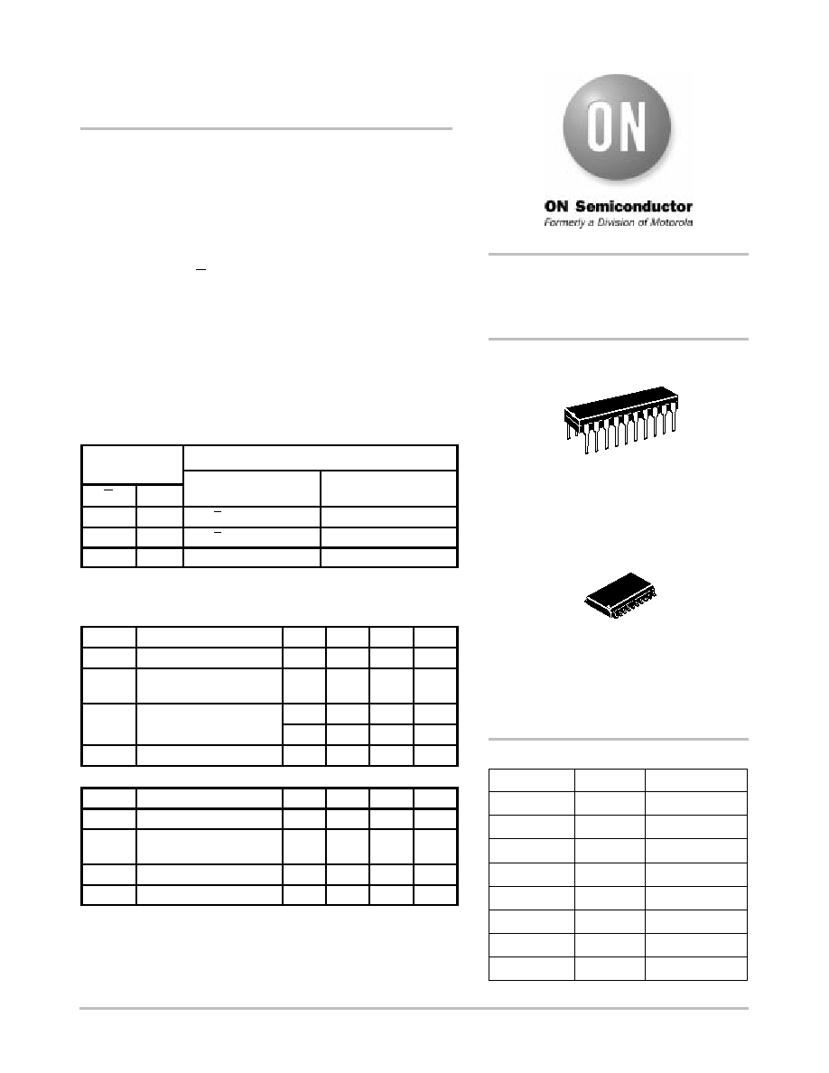
ORDERING INFORMATION
SN74LS640N
16 Pin DIP
1440 Units/Box
SN74LS640DW
16 Pin
SOIC
DW SUFFIX
CASE 751D
http://onsemi.com
2500/Tape & Reel
PLASTIC
N SUFFIX
CASE 738
20
1
20
1
SN74LS641N
16 Pin DIP
1440 Units/Box
SN74LS641DW
16 Pin
2500/Tape & Reel
SN74LS642N
16 Pin DIP
1440 Units/Box
SN74LS642DW
16 Pin
2500/Tape & Reel
SN74LS645N
16 Pin DIP
1440 Units/Box
SN74LS645DW
16 Pin
2500/Tape & Reel
SN74LS640 SN74LS641 SN74LS642 SN74LS645
http://onsemi.com
2
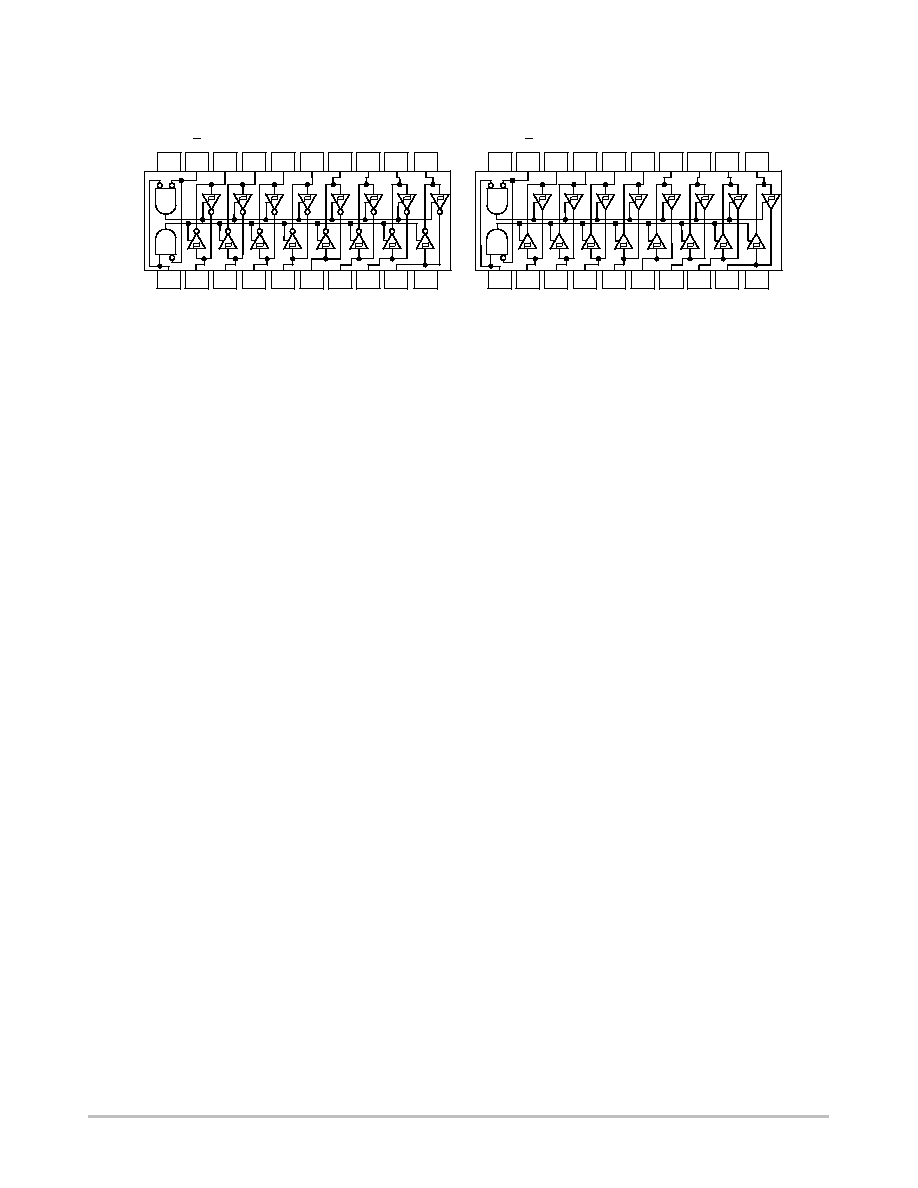
CONNECTION DIAGRAMS DIP (TOP VIEW)
18
17
16
15
14
13
1
2
3
4
5
6
7
20
19
8
V
CC
DIR
B1
B2
B3
B5
B4
B6
A1
A2
A3
A4
A5
A6
A7
9
10
A8
GND
12
11
B7
B8
18
17
16
15
14
13
1
2
3
4
5
6
7
20
19
8
V
CC
DIR
B1
B2
B3
B5
B4
B6
A1
A2
A3
A4
A5
A6
A7
9
10
A8
GND
12
11
B7
B8
SN74LS640
SN74LS642
SN74LS641
SN74LS645
ENABLE
G
ENABLE
G
SN74LS640 SN74LS641 SN74LS642 SN74LS645
http://onsemi.com
3
SN74LS640
∑
SN74LS645
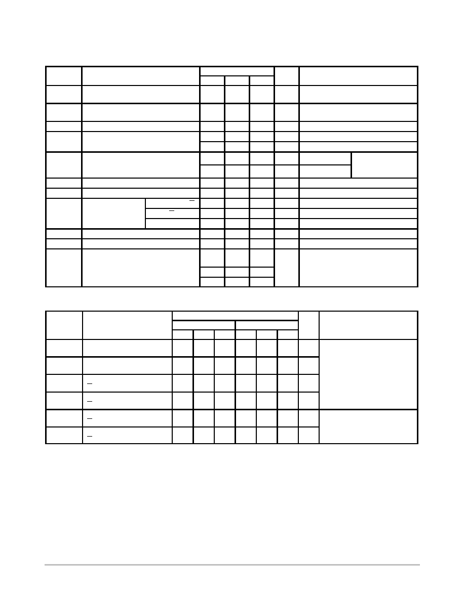
DC CHARACTERISTICS OVER OPERATING TEMPERATURE RANGE
(unless otherwise specified)
Limits
Symbol
Parameter
Min
Typ
Max
Unit
Test Conditions
V
IH
Input HIGH Voltage
2.0
V
Guaranteed Input HIGH Voltage for
All Inputs
V
IL
Input LOW Voltage
0.6
V
Guaranteed Input LOW Voltage for
All Inputs
V
IK
Input Clamp Diode Voltage
≠ 0.65
≠ 1.5
V
V
CC
= MIN, I
IN
= ≠ 18 mA
V
O
Output HIGH Voltage
2.4
3.4
V
V
CC
= MIN, I
OH
= 3.0 mA
V
OH
Output HIGH Voltage
2.0
V
V
CC
= MIN, I
OH
= MAX
V
O
Output LOW Voltage
0.25
0.4
V
I
OL
= 12 mA
V
CC
= V
CC
MIN,
V
IN
= V
IL
or V
IH
V
OL
Output LOW Voltage
0.35
0.5
V
I
OL
= 24 mA
V
IN
= V
IL
or V
IH
per Truth Table
I
OZH
Output Off Current HIGH
20
µ
A
V
CC
= MAX, V
OUT
= 2.7 V
I
OZL
Output Off Current LOW
≠ 400
µ
A
V
CC
= MAX, V
OUT
= 0.4 V
A or B, DIR or G
20
µ
A
V
CC
= MAX, V
IN
= 2.7 V
I
IH
Input HIGH Current
DIR or G
0.1
mA
V
CC
= MAX, V
IN
= 7.0 V
A or B
0.1
mA
V
CC
= MAX, V
IN
= 5.5 V
I
IL
Input LOW Current
≠ 0.4
mA
V
CC
= MAX, V
IN
= 0.4 V
I
OS
Output Short Circuit Current (Note 1)
≠ 40
≠ 225
mA
V
CC
= MAX
I
Power Supply Current
Total Output HIGH
70
mA
V
MAX
I
CC
Total, Output LOW
90
mA
V
CC
= MAX
Total at HIGH Z
95
Note 1: Not more than one output should be shorted at a time, nor for more than 1 second.
AC CHARACTERISTICS
(T
A
= 25
∞
C, V
CC
= 5.0 V)
Limits
LS640
LS645
Symbol
Parameter
Min
Typ
Max
Min
Typ
Max
Unit
Test Conditions
t
PLH
t
PHL
Propagation Delay
A to B
6.0
8.0
10
15
8.0
11
15
15
ns
t
PLH
t
PHL
Propagation Delay
B to A
6.0
8.0
10
15
8.0
11
15
15
ns
C
L
= 45 pF,
t
PZL
t
PZH
Output Enable Time
G, DIR to A
31
23
40
40
31
26
40
40
ns
L
R
L
= 667
t
PZL
t
PZH
Output Enable Time
G, DIR to B
31
23
40
40
31
26
40
40
ns
t
PLZ
t
PHZ
Output Disable Time
G, DIR to A
15
15
25
25
15
15
25
25
ns
C = 5 0 pF
t
PLZ
t
PHZ
Output Disable Time
G, DIR to B
15
15
25
25
15
15
25
25
ns
C
L
= 5.0 pF
SN74LS640 SN74LS641 SN74LS642 SN74LS645
http://onsemi.com
4
SN74LS641
∑
SN74LS642
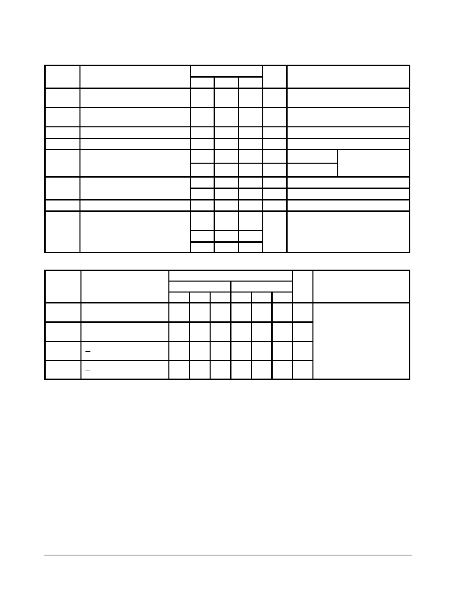
DC CHARACTERISTICS OVER OPERATING TEMPERATURE RANGE
(unless otherwise specified)
Limits
Symbol
Parameter
Min
Typ
Max
Unit
Test Conditions
V
IH
Input HIGH Voltage
2.0
V
Guaranteed Input HIGH Voltage for
All Inputs
V
IL
Input LOW Voltage
0.6
V
Guaranteed Input LOW Voltage for
All Inputs
V
IK
Input Clamp Diode Voltage
≠ 0.65
≠ 1.5
V
V
CC
= MIN, I
IN
= ≠ 18 mA
I
OH
Output HIGH Current
100
µ
A
V
CC
= MIN, V
OH
= MAX
V
O
Output LOW Voltage
0.25
0.4
V
I
OL
= 12 mA
V
CC
= V
CC
MIN,
V
IN
= V
IL
or V
IH
V
OL
Output LOW Voltage
0.35
0.5
V
I
OL
= 24 mA
V
IN
= V
IL
or V
IH
per Truth Table
I
Input HIGH Current
20
µ
A
V
CC
= MAX, V
IN
= 2.7 V
I
IH
Input HIGH Current
≠0.1
mA
V
CC
= MAX, V
IN
= 7.0 V
I
IL
Input LOW Current
≠ 0.4
mA
V
CC
= MAX, V
IN
= 0.4 V
I
Power Supply Current
Total, Output HIGH
70
A
V
MAX
I
CC
Total, Output LOW
90
mA
V
CC
= MAX
Total at HIGH Z
95
AC CHARACTERISTICS
(T
A
= 25
∞
C, V
CC
= 5.0 V)
Limits
LS641
LS642
Symbol
Parameter
Min
Typ
Max
Min
Typ
Max
Unit
Test Conditions
t
PLH
t
PHL
Propagation Delay,
A to B
17
16
25
25
19
14
25
25
ns
t
PLH
t
PHL
Propagation Delay,
B to A
17
16
25
25
19
14
25
25
ns
C
L
= 45 pF,
t
PLH
t
PHL
Propagation Delay,
G, DIR to A
23
34
40
50
26
43
40
60
ns
L
R
L
= 667
t
PLH
t
PHL
Propagation Delay,
G, DIR to B
25
37
40
50
28
39
40
60
ns
SN74LS640 SN74LS641 SN74LS642 SN74LS645
http://onsemi.com
5
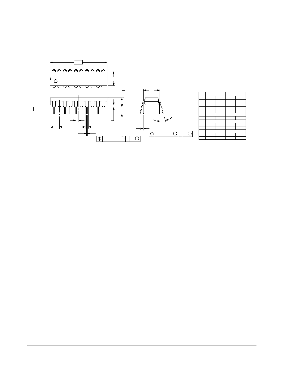
PACKAGE DIMENSIONS
N SUFFIX
PLASTIC PACKAGE
CASE 738≠03
ISSUE E
NOTES:
1. DIMENSIONING AND TOLERANCING PER ANSI
Y14.5M, 1982.
2. CONTROLLING DIMENSION: INCH.
3. DIMENSION L TO CENTER OF LEAD WHEN
FORMED PARALLEL.
4. DIMENSION B DOES NOT INCLUDE MOLD
FLASH.
M
L
J
20 PL
M
B
M
0.25 (0.010)
T
DIM
MIN
MAX
MIN
MAX
MILLIMETERS
INCHES
A
25.66
27.17
1.010
1.070
B
6.10
6.60
0.240
0.260
C
3.81
4.57
0.150
0.180
D
0.39
0.55
0.015
0.022
G
2.54 BSC
0.100 BSC
J
0.21
0.38
0.008
0.015
K
2.80
3.55
0.110
0.140
L
7.62 BSC
0.300 BSC
M
0
15
0
15
N
0.51
1.01
0.020
0.040
_
_
_
_
E
1.27
1.77
0.050
0.070
1
11
10
20
≠A≠
SEATING
PLANE
K
N
F
G
D
20 PL
≠T≠
M
A
M
0.25 (0.010)
T
E
B
C
F
1.27 BSC
0.050 BSC
SN74LS640 SN74LS641 SN74LS642 SN74LS645
http://onsemi.com
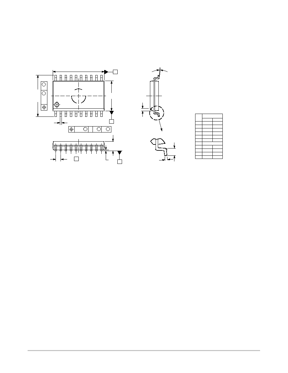
6
PACKAGE DIMENSIONS
D SUFFIX
PLASTIC SOIC PACKAGE
CASE 751D≠05
ISSUE F
20
1
11
10
B
20X
H
10X
C
L
18X
A1
A
SEATING
PLANE
q
h
X 45
_
E
D
M
0.25
M
B
M
0.25
S
A
S
B
T
e
T
B
A
DIM
MIN
MAX
MILLIMETERS
A
2.35
2.65
A1
0.10
0.25
B
0.35
0.49
C
0.23
0.32
D
12.65
12.95
E
7.40
7.60
e
1.27 BSC
H
10.05
10.55
h
0.25
0.75
L
0.50
0.90
q
0
7
NOTES:
1. DIMENSIONS ARE IN MILLIMETERS.
2. INTERPRET DIMENSIONS AND TOLERANCES
PER ASME Y14.5M, 1994.
3. DIMENSIONS D AND E DO NOT INCLUDE MOLD
PROTRUSION.
4. MAXIMUM MOLD PROTRUSION 0.15 PER SIDE.
5. DIMENSION B DOES NOT INCLUDE DAMBAR
PROTRUSION. ALLOWABLE PROTRUSION SHALL
BE 0.13 TOTAL IN EXCESS OF B DIMENSION AT
MAXIMUM MATERIAL CONDITION.
_
_

SN74LS640 SN74LS641 SN74LS642 SN74LS645
http://onsemi.com
7
Notes
SN74LS640 SN74LS641 SN74LS642 SN74LS645
http://onsemi.com
8
ON Semiconductor and are trademarks of Semiconductor Components Industries, LLC (SCILLC). SCILLC reserves the right to make changes
without further notice to any products herein. SCILLC makes no warranty, representation or guarantee regarding the suitability of its products for any particular
purpose, nor does SCILLC assume any liability arising out of the application or use of any product or circuit, and specifically disclaims any and all liability,
including without limitation special, consequential or incidental damages. "Typical" parameters which may be provided in SCILLC data sheets and/or
specifications can and do vary in different applications and actual performance may vary over time. All operating parameters, including "Typicals" must be
validated for each customer application by customer's technical experts. SCILLC does not convey any license under its patent rights nor the rights of others.
SCILLC products are not designed, intended, or authorized for use as components in systems intended for surgical implant into the body, or other applications
intended to support or sustain life, or for any other application in which the failure of the SCILLC product could create a situation where personal injury or
death may occur. Should Buyer purchase or use SCILLC products for any such unintended or unauthorized application, Buyer shall indemnify and hold
SCILLC and its officers, employees, subsidiaries, affiliates, and distributors harmless against all claims, costs, damages, and expenses, and reasonable
attorney fees arising out of, directly or indirectly, any claim of personal injury or death associated with such unintended or unauthorized use, even if such claim
alleges that SCILLC was negligent regarding the design or manufacture of the part. SCILLC is an Equal Opportunity/Affirmative Action Employer.
PUBLICATION ORDERING INFORMATION
ASIA/PACIFIC: LDC for ON Semiconductor ≠ Asia Support
Phone:
303≠675≠2121 (Tue≠Fri 9:00am to 1:00pm, Hong Kong Time)
Toll Free from Hong Kong 800≠4422≠3781
Email: ONlit≠asia@hibbertco.com
JAPAN: ON Semiconductor, Japan Customer Focus Center
4≠32≠1 Nishi≠Gotanda, Shinagawa≠ku, Tokyo, Japan 141≠8549
Phone: 81≠3≠5487≠8345
Email: r14153@onsemi.com
Fax Response Line:
303≠675≠2167
800≠344≠3810 Toll Free USA/Canada
ON Semiconductor Website: http://onsemi.com
For additional information, please contact your local
Sales Representative.
SN74LS640/D
North America Literature Fulfillment:
Literature Distribution Center for ON Semiconductor
P.O. Box 5163, Denver, Colorado 80217 USA
Phone: 303≠675≠2175 or 800≠344≠3860 Toll Free USA/Canada
Fax: 303≠675≠2176 or 800≠344≠3867 Toll Free USA/Canada
Email: ONlit@hibbertco.com
N. American Technical Support: 800≠282≠9855 Toll Free USA/Canada
EUROPE: LDC for ON Semiconductor ≠ European Support
German Phone: (+1) 303≠308≠7140 (M≠F 2:30pm to 5:00pm Munich Time)
Email: ONlit≠german@hibbertco.com
French Phone: (+1) 303≠308≠7141 (M≠F 2:30pm to 5:00pm Toulouse Time)
Email: ONlit≠french@hibbertco.com
English Phone: (+1) 303≠308≠7142 (M≠F 1:30pm to 5:00pm UK Time)
Email: ONlit@hibbertco.com