 | –≠–ª–µ–∫—Ç—Ä–æ–Ω–Ω—ã–π –∫–æ–º–ø–æ–Ω–µ–Ω—Ç: AND8066 | –°–∫–∞—á–∞—Ç—å:  PDF PDF  ZIP ZIP |
©
Semiconductor Components Industries, LLC, 2002
May, 2002 ≠ Rev. 2
1
Publication Order Number:
AND8066/D
AND8066/D
Interfacing with ECLinPS
Prepared by: Paul Shockman
ON Semiconductor Logic Applications Engineering
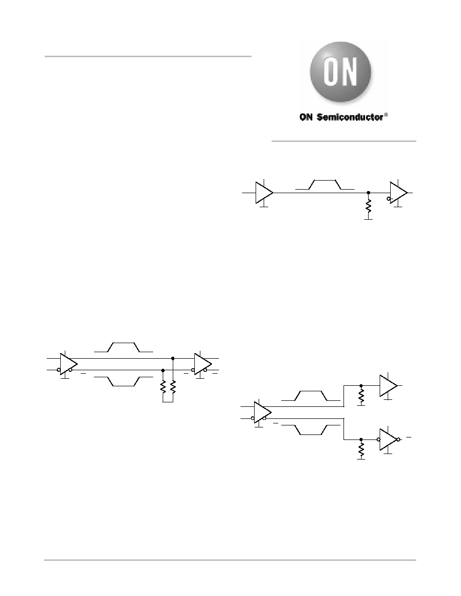
STANDARD ECL INTERFACE: DIFFERENTIAL
DRIVER AND RECEIVER
A typical Emitter Coupled Logic (ECL) circuit interface
may be defined as a differential driver device sending a paired
set of commentary signals ≠ True and Invert ≠ over a pair of
standard, controlled impedance lines to an ECL differential
receiver device. A typical ECL output line driver consists of
a bipolar transistor in an Emitter Follower configuration with
the collector at V
CC
power supply rail and the emitter pinned
out. A standard, typical differential ECL receiver consists of
a pair of bipolar transistors in a differential configuration with
the True and Invert signals providing base drives to the two
base inputs. Proper differential levels are specified as V
pp
and
V
IHCMR
. When an input is interconnected as a differential
signal, the DC Single Ended parameters of V
IL
and V
IH
do not
apply. Terminations are required to preserve optimum signal
integrity, as shown in Figure 1. The standard, controlled
impedance lines assume a sufficient return current capability.
V
EE
V
CC
V
EE
V
TT
V
CC
Figure 1. Standard Differential ECL Interconnect
Q
Q
Q
Q
D
D
True
Invert
SINGLE≠ENDED INTERFACE
Signals may be imported as full differential lines or as a
Single≠Ended (SE) line interconnection. The SE
interconnection may be seen as a special variation of the
typical differential interface using only one driver source
trace line. This single trace line drives a (Base) input pin of
the receiver, as shown in Figure 2. Although a receiver may
present only a single, dedicate SE input pin instead of a
differential input pair of pins, such a receiver still would have
a differential structure with the unavailable input controlled
by internal circuitry.
V
EE
V
CC
V
EE
Figure 2. Standard Single≠Ended ECL Interconnect
True
V
TT
V
CC
Single≠ended receiver input levels are specified in data
sheets DC CHARACTERISTICS block as V
IH
and V
IL
Parameters. Each temperature has a minimum and
maximum limit pair to V
IH
and V
IL
parameters, thus
defining the Single≠Ended input swing, V
pp
(SE). The
V
pp
(SE) ranges from 595 mV to 890 mV, depending on the
temperature and family. The V
pp
(SE) limits constitute the
receiver device's input single≠ended sensitivity.
Both output lines of the typical differential output may
drive two independent single≠ended receivers separately (see
Figure 3).
V
EE
V
CC
V
EE
Figure 3. Differential Driver with Independent
Standard Single≠Ended Receivers
True
V
TT
V
CC
Invert
V
EE
V
CC
V
TT
Q
Q
Q
Q
APPLICATION NOTE
http://onsemi.com
AND8066/D
http://onsemi.com
2
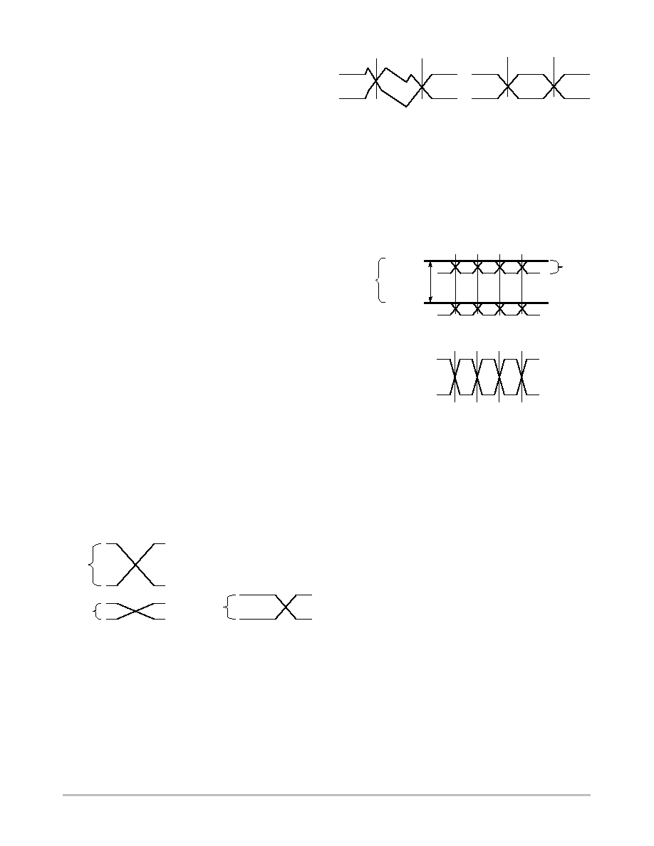
V
BB
Reference
For a standard differential receiver with two input pins ≠
D and D ≠ only one of two inputs is suitably selected to
receive the signal while the non≠driven input must be biased
to a (DC) reference voltage, V
BB
(see Figure 4).
V
EE
V
CC
V
EE
Figure 4. Standard SE Receivers with V
BB
True
V
BB
V
CC
V
TT
Q
Q
Q
D
D
The V
BB
value is designed to be maintained midway
(50%) between the HIGH and LOW levels of the received
signal, that is, the crosspoint voltage of a differential signal
pair, to preserve the duty cycle and signal integrity (see
Figure 5).
V
BB
or Crosspoint
Figure 5. V
BB
Crosspoint Voltage
True
Invert
LOW
HIGH
If V
BB
shifts, due to drift or noise, above the input signal
50% crosspoint, the device output signal will shift the duty
cycle away from a pure 50% point to a decreased, narrowing
pulse width (see Figure 6).
Figure 6.
D
V
BB
Input
HIGH
LOW
Output Shift Narrower
If V
BB
shifts below the input signal 50% crosspoint, the
device output signal will shift the duty cycle away from a
pure 50% point to an increased, widening pulse width (see
Figure 7).
Figure 7.
D
V
BB
Input
HIGH
LOW
Output Shift Wider
Obviously, any error voltage present on the V
BB
reference
level injects jitter directly into the signal.
V
BB
: Voltage Reference Sources
A V
BB
reference voltage output source pin may be available
on the receiver device. When present, V
BB
is an internally
generated voltage supply and available only to that device's
inputs. Current demand on the V
BB
pin should be limited to 0.5
mA. Bypass (0.01
mF) V
BB
to the quietest plane, usually V
CC
,
since noise on V
BB
will inject jitter and corrupt duty cycle. The
V
BB
voltage is derived from referencing the V
CC
supply and
will track changes in V
CC
100% or 1:1. If V
CC
shifts 1 mV,
then V
BB
also changes 1 mV. Changes in V
EE
also affect the
V
BB
voltage and will track at the rate of 0 to 20%, typically 5%.
If V
EE
shifts 100 mV, then V
BB
follows with a 0 mV to 20 mV
shift of the same polarity, typically 5 mV.
A V
BB
reference voltage may be generated off≠device and
supplied to the input pins. Ripple content must be kept as low
as possible on V
CC
since it transfers to the signal as jitter and
phase error. A V
BB
voltage reference level may be supplied
from a V
BB
generator, as shown in Figure 8. Any of the "16"
type buffers are recommended to produce a high current gain
V
BB
buffer. For example, the E416, EL16, LVEL16, EP16,
LVEP16, EL17, LVEL17, etc. type devices have a V
BB
pin
available. A 1 K
W resistor may be needed the feedback path
to stabilize higher gain buffers.
Figure 8. V
BB
Voltage Reference Generator
V
BB(out)
16
RT
V
TT
V
CC
or V
TT
V
BB
0.01
m
F
1 K
W
AND8066/D
http://onsemi.com
3
Depending on system requirements, V
BB
may be
generated by a dedicated supply, a "16" type buffer, or by
using a bypassed resistor voltage divider.
Dedicated Single≠Ended Input Structure
A device may have a dedicated single≠ended input, having
only one of the internal differential base inputs pinned out of the
package, available to be driven by a signal. Internal circuitry
connects a V
BB
voltage reference to the other internal,
non≠driven input base node of the differential buffer gate, as
shown in Figure 2. This internal, fixed reference voltage, V
BB
,
is maintained at the midpoint between V
IL
and V
IH
for
dedicated single≠ended inputs. The internal V
BB
is derived from
referencing the V
CC
supply and tracks changes 1:1 in this
supply. Noise and drift in V
CC
will inject jitter and phase noise
directly into the signal.
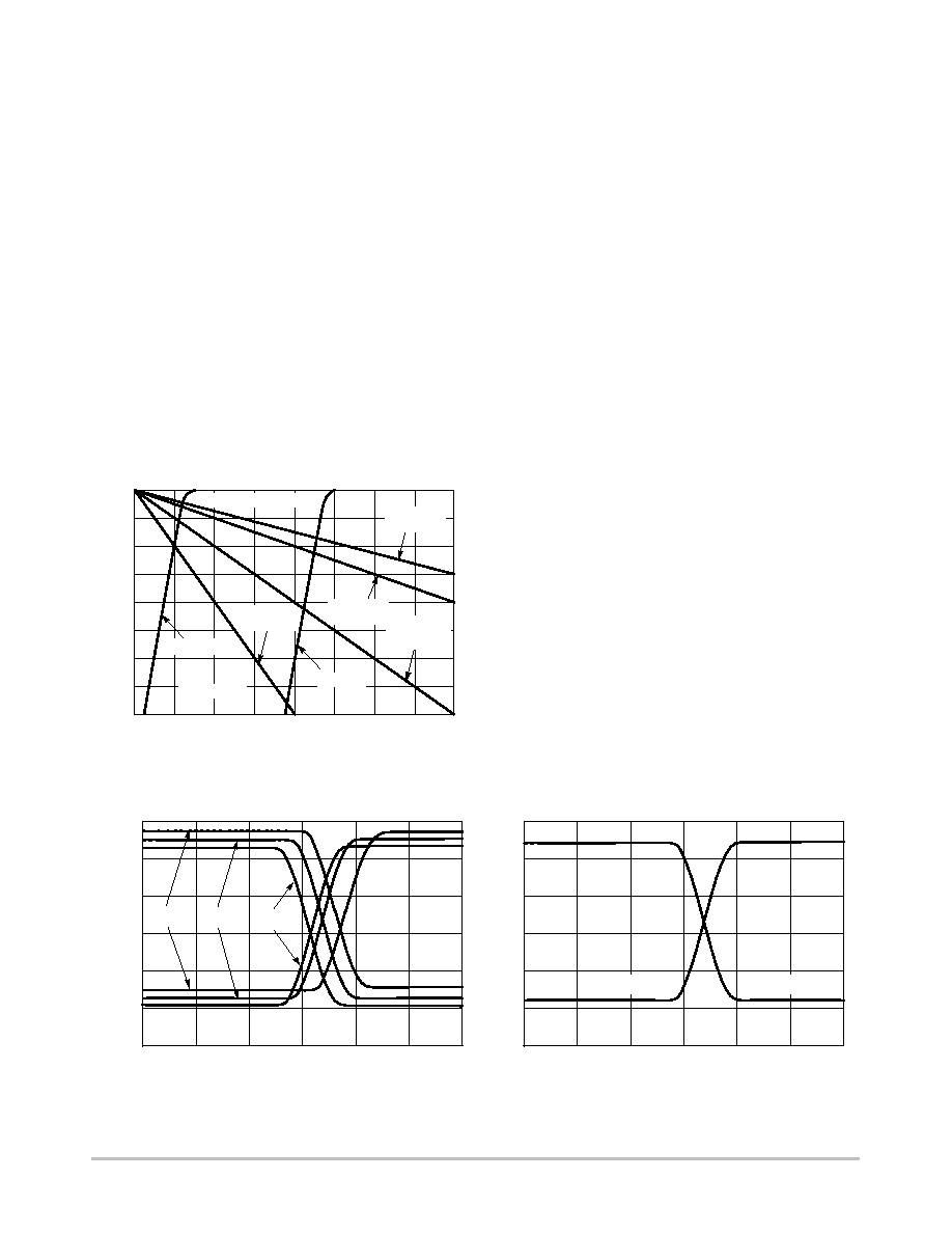
DIFFERENTIAL INTERFACE
A standard differential interconnect driver signal will be
received as signal swing. Historically, standard ECL driver
signal swing may range from 750 mV to 1040 mV depending
on the family, although 800 mV is typical. Newer devices may
offer RSECL (Reduced Swing ECL) or Variable Output Swing
(NBSG16VS). Receiver sensitivity is specified by data sheets as
the input swing voltage peak≠to≠peak (V
pp
). Proper output
operation is displayed as the typical amplitude through the entire
range of input swing, from minimum to maximum as shown in
Figure 9: V
pp
≠ Input Swing Voltage Peak≠to≠Peak. Input
swings greater than specification limit maximum may cause
degraded frequency performance and increased t
pd
input. Input
swings less than specification minimum will cause diminished
output amplitude due to the device voltage gain and low enough
input amplitude will result in a loss of output signal. All
waveforms are measured with single ended probes with
reference to ground (not as a differential probe value). Operation
in the small signal level range less than V
pp
minimum display
a characteristic gain and may obviously be operated as a limited
linear amplifier this input swing range.
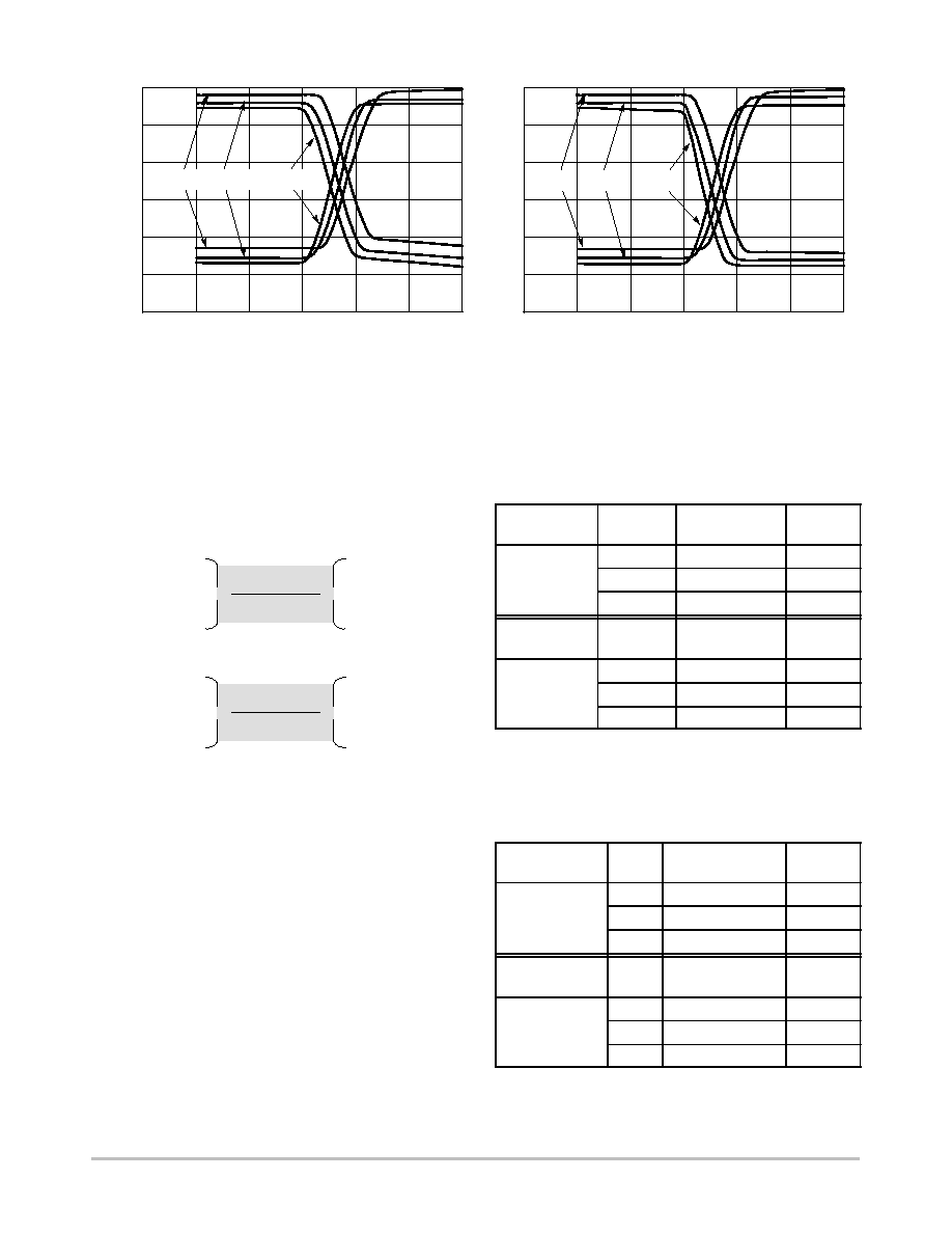
Figure 9. V
pp
≠ Input Swing Voltage Peak≠to≠Peak
Input V
pp
Output V
pp
Max
Min
Typ
Noise common to both differential lines and within the input
operating range will be rejected and ignored by the receiver.
The transfer threshold point is determined by the crosspoint of
the differential signal. A voltage shift in input operating range
of the transfer point has no voltage or timing effect on the
signal, therefore, preserving integrity. A receiver's tolerance of
common mode interference is illustrated in Figure 10.
Figure 10. Differential Input High Noise Immunity
t
1
t
2
t
1
t
2
Input
Output
V
IHCMR
Each input signal to a differential pair receiver will display a
Vin HIGH voltage (V
IH
) level and a Vin LOW voltage V
IL
.
Proper operation is achieved when the Vin HIGH voltage (V
IH
)
level falls within spec limits, V
IHCMR
(Voltage Input High
Common Mode Range) minimum to maximum as represented
in Figure 11.
Figure 11. V
IH
Common Mode Range, V
IHCMR
V
IN(pp)
t
1
t
2
t
3
t
4
V
IH(max)
V
IH(min)
V
IHCMR
Input
t
1
t
2
t
3
t
4
V
OUT(pp)
Output
Considerations for Single≠Ended and Differential
Interconnects
Several advantages and disadvantages are listed below.
Single≠Ended (SE) Interconnects
Advantages may include:
∑
Decreased board real estate routing.
∑
Reduced system power demand.
Disadvantages may include:
∑
Higher jitter, phase error, and duty cycle skew.
∑
High noise sensitivity.
∑
Critically narrow interface windows.
∑
Poor receiver sensitivity.
∑
Higher EMI emission.
Differential Interconnects
Advantages may include:
∑
High common mode noise rejection (low noise
sensitivity).
AND8066/D
http://onsemi.com
4
∑
Wide signal interface windows.
∑
High receiver sensitivity.
∑
Low EMI emission.
Disadvantages may include:
∑
Increased board routing real estate.
∑
Increased system power demand.
ECL 10 and 100 Performance Standards
There currently exist two basic legacy standards for high
performance ECL logic devices.
10 Series (compatible with 10H)
100 Series (compatible with 100K)
Both standards display similar highly compatible output
amplitude swings of about 800 mV
pp
over a wide range of
operating conditions and loads. This is due to drivers
enjoying a remaining internal output impedance ranging
from 6 to 8
W in both HIGH and LOW level state levels (see
Figure 12).
Figure 12. Outputs vs. Load Drive Characteristics
25
W
to ≠2.0 V
≠2.0
0
≠5
≠10
≠15
≠0.75
≠1.0
≠1.25
≠20
≠25
≠30
≠35
≠40
≠1.75
≠0.5 ≠0.25
0
OUTPUT VOLTAGE (V)
OUTPUT CURRENT (mA)
SLOPE = 6
W
≠ 8
W
V
OH
≠1.5
V
OL
T
A
= 25
∞
C
50
W
to ≠2.0 V
150
W
to ≠2.0 V
100
W
to ≠2.0 V
For loads of 35 ohms or less, outputs may need to be
"ganged" (wire "ANDed"), or specialized 25≠
W driver
circuits deployed. These specialized drivers ensure reduced
power dissipation and improve long term reliability. Both
standards display similar rise/fall times, propagation delays,
and toggle frequencies.
Differential Interface Between 10 and 100
Standards
When interfacing differentially, the two basic standards
are completely, directly compatible over all operational
conditions. This results from receivers of both standards
exhibiting wide V
IH
Common Mode Range and fine
minimum input sensitivity, V
pp
. Output temperature
variations associated with 10 Series devices are well within
these receiver input characteristic limitations.
Single≠Ended (SE) Interface Between 10 and 100
Standards
Single≠Ended (SE) line signal interconnects require
analysis of both the driver output levels, V
OH
and V
OL
,
across temperature and the receiver input voltage level
limits, V
IH
and V
IL
, to determine complete interface
compatibility. Although 100 Series standard devices
incorporate a temperature compensation network in the
output driver, some variation may still be observed.
Variation of the driver output levels, V
OH
and V
OL
, across
temperature is typically present in 10 Series devices.
Device series voltage transfer curves characterize the
input and output behavior function across temperature. This
is shown in Figures 13 through 16 for 10E, 100E, 10K, and
10KH Series. Changes in technology refinements to the 10K
Series led to the 10KH Series with better performance in V
IH
and V
OL
as V
in
approached V
CC
. the 10E Series is similar
to the 10KH Series. Temperature compensation allowed the
development of the 100 Series.
≠2.0
≠1.2
≠1.4
≠1.8
≠1.6
≠1.8
V
out
, RELA
TIVE T
O
V
CC
V
in
, (RELATIVE TO V
CC
)
V
out
, RELA
TIVE T
O
V
CC
≠0.8
25
∞
C
V
in
, (RELATIVE TO V
CC
)
≠1.6
≠1.4
≠1.0
≠1.2
≠0.8
≠1.0
≠2.0
≠1.2
≠1.4
≠1.8
≠1.6
≠1.8
≠0.8
≠1.6
≠1.4
≠1.0
≠1.2
≠0.8
≠1.0
25
∞
C
25
∞
C
0
∞
C
85
∞
C
Figure 13. 10E Series Vin vs. Vout Transfer Curves
Figure 14. 100E Series Vin vs. Vout Transfer Curves
AND8066/D
http://onsemi.com
5
V
in
, (RELATIVE TO V
CC
)
V
in
, (RELATIVE TO V
CC
)
V
out
, RELA
TIVE T
O
V
CC
V
out
, RELA
TIVE T
O
V
CC
≠1.2
≠1.8
≠0.8
≠1.6
≠1.4
≠1.0
≠1.2
≠1.8
≠0.8
≠1.6
≠1.4
≠1.0
≠2.0
≠1.4
≠1.6
≠1.8
≠1.2
≠0.8
≠1.0
≠2.0
≠1.4
≠1.6
≠1.8
≠1.2
≠0.8
≠1.0
85
∞
C
25
∞
C
≠30
∞
C
70
∞
C
25
∞
C
0
∞
C
Figure 15. 10K Series Vin vs. Vout Transfer Curves
Figure 16. 10KH Series Vin vs. Vout Transfer Curves
The difference in the DC behavior of the inputs and outputs
of the two different standards necessitates caution when
mixing the two technologies in single≠ended designs. Output
levels become critical to the receiver when the V
OH
minimum,
V
OHA
, drives into the receiver as the V
IH
minimum. Levels are
also critical when the driver V
OL
maximum, V
OLA
, drives into
the receiver as the V
IL
maximum.
Figure 17. Single≠Ended Noise Margin
V
OH(max)
V
OH(min)
V
OHA
V
IH(max)
V
IH(min)
V
OL(max)
V
OLA
V
OL(min)
V
IL(max)
V
IH(min)
Noise margin quantifies the susceptibility of a driver and
receiver interface to any non≠signal voltage levels and
therefore risking false switching. Two measurements ≠
NOISE MARGIN HIGH and NOISE MARGIN LOW ≠
describe the false switching risk across temperature as
follows:
NOISE MARGIN
(HIGH)
= V
OH(min)
≠ V
IH(min)
NOISE MARGIN
(LOW)
= V
OL(max)
≠ V
IL(max)
An MC10EP16DT, operating in LVPECL mode with 3.3 V
on V
CC
and 0.0 V on V
EE
, interfaced to an MC10EP16DT
receiver, single≠ended, has a noise margin at the specification
ambient temperature shown in Table 1. Notice the safety
margin levels are positive for NOISE MARGIN HIGH
indicating the driver exceeds the receiver's requirement for a
minimum and the delta is positive. For a NOISE MARGIN
LOW, the driver must be below the receiver's maximum and
the delta is negative.
Table 1. Noise Margins: MC10EP16DT Interfaced to
an MC10EP16DT Receiver
10 to 10 Noise
Margin HIGH
Temp.
V
OH(min)
≠
V
IH(min)
Delta
(mV)
≠40
∞
C
2165 ≠ 2090
75
25
∞
C
2230 ≠ 2155
75
85
∞
C
2290 ≠ 2215
75
10 to 10 Noise
Margin LOW
Temp.
V
OL(max)
≠
V
IL(max)
Delta
(mV)
≠40
∞
C
1615 ≠ 1690
≠40
25
∞
C
1680 ≠ 1755
≠75
85
∞
C
1740 ≠ 1810
≠70
When a 10 Series device drives a 100 Series device
single≠ended, the noise margins become a risk factor requiring
careful evaluation as indicated in Table 2.
Table 2. Noise Margins: MC10EP16DT Interfaced to
an MC100EP16DT Receiver
10 to 100 Noise
Margin HIGH
Temp.
V
OH(min)
≠ V
IH(min)
Delta
(mV)
≠40
∞
C
2165 ≠ 2075
90
25
∞
C
2230 ≠ 2075
155
85
∞
C
2290 ≠ 2075
215
10 to 100 Noise
Margin LOW
Temp.
V
OL(max)
≠ V
IL(max)
Delta
(mV)
≠40
∞
C
1615 ≠ 1675
≠60
25
∞
C
1680 ≠ 1675
5
85
∞
C
1740 ≠ 1675
65
AND8066/D
http://onsemi.com
6
When a 100 Series device drives a 10 Series device,
single≠ended, the noise margins are very robust and immunity
is optimized (See Table 3).
Table 3. Noise Margins: MC100EP16DT Interfaced to
an MC10EP16DT Receiver
100 to 10 Noise
Margin HIGH
Temp.
V
OH(min)
≠ V
IH(min)
Delta
(mV)
≠40
∞
C
2405 ≠ 2090
315
25
∞
C
2405 ≠ 2155
250
85
∞
C
2405 ≠ 2215
190
100 to 10 Noise
Margin LOW
Temp.
V
OL(max)
≠ V
IL(max)
Delta
(mV)
≠40
∞
C
1605 ≠ 1690
≠85
25
∞
C
1605 ≠ 1755
≠150
85
∞
C
1605 ≠ 1810
≠205
Edge Rates (dV/dT)
As a driver rising edge approaches the transfer voltage
point of the receiver input, the receiver diminishes in voltage
according to the small signal gain of the device. When the
input voltage level passes through the transfer crosspoint, the
output will "switch" states in an analog or operational
amplifier mode. Non≠signal voltage fluctuations and noise
will be amplified. These phenomena will determine the
suitable edge rate limitation. As the edge becomes slower,
ambient noise present on the input pin will typically constrain
practical usability. Typically, this may be from 5 ns to 35 ns
and further precaution, such as shielding, will extend the
operating edge times.
For signal edges slower than 20 ns, a Schmitt trigger circuit
may be considered to reliably sharpen the edge rates. In
theory, ECL logic may operate from sub≠hertz (< 1.0 Hz)
frequencies, but real circuit conditions will constrain practical
limits.
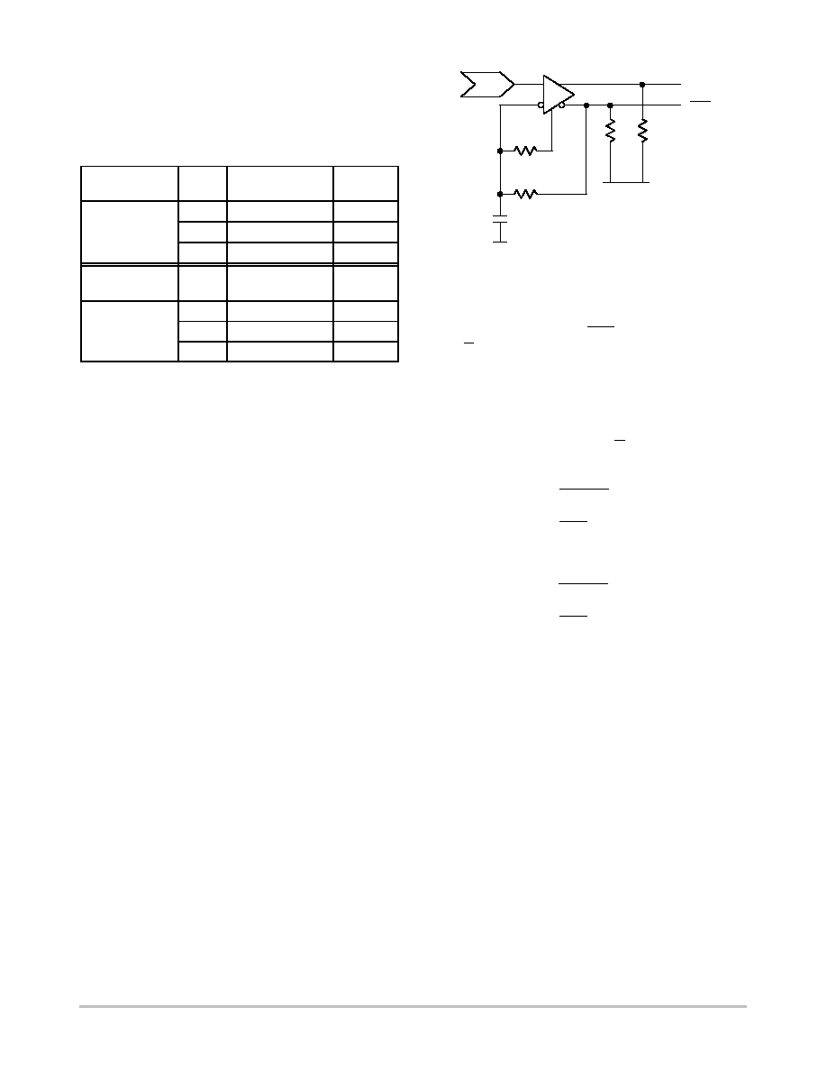
Figure 18. Schmitt Trigger with 228 mV Hysteresis
Q
out
16
RT
V
TT
V
CC
or V
TT
V
BB
0.01
m
F
RT
R2
400
W
R1
1 k
W
D
IN
Q
out
Schmitt conditioning may be determined by the resistor
values. An R1 resistor of 1 k
W provides inverted output
feedback resistor (R
fb
) from Qout to the threshold voltage
point, D. A 400
W bias resistor, R2, to V
BB
sets the voltage
offset as a fraction of the output voltage from V
BB
. With an
800 mV V
out
swing, V
BB
will be the midpoint between V
OH
and V
OL
, or 400 mV from a state level. The two resistors
form a voltage divider from either state level to V
BB
.About
28% of the LOW or HIGH state level is developed at the
voltage divider node and ported to D. This will be the offset
a signal must exceed to force the buffer to switch states.
For tr Voffset
+
R2
R1
)
R2
<
( VOL
*
VBB )
+
400
1400
<
400
+
114mV
For tf Voffset
+
R2
R1
)
R2
<
( VOH
*
VBB )
+
400
1400
<
400
+
114mV
This creates a total of 228 mV of hysteresis conditioning.
The effect of the hysteresis delay in a signal must be
considered in the timing analysis.

AND8066/D
http://onsemi.com
7
Notes
AND8066/D
http://onsemi.com
8
ON Semiconductor and are registered trademarks of Semiconductor Components Industries, LLC (SCILLC). SCILLC reserves the right to make
changes without further notice to any products herein. SCILLC makes no warranty, representation or guarantee regarding the suitability of its products for any
particular purpose, nor does SCILLC assume any liability arising out of the application or use of any product or circuit, and specifically disclaims any and all
liability, including without limitation special, consequential or incidental damages. "Typical" parameters which may be provided in SCILLC data sheets and/or
specifications can and do vary in different applications and actual performance may vary over time. All operating parameters, including "Typicals" must be
validated for each customer application by customer's technical experts. SCILLC does not convey any license under its patent rights nor the rights of others.
SCILLC products are not designed, intended, or authorized for use as components in systems intended for surgical implant into the body, or other applications
intended to support or sustain life, or for any other application in which the failure of the SCILLC product could create a situation where personal injury or death
may occur. Should Buyer purchase or use SCILLC products for any such unintended or unauthorized application, Buyer shall indemnify and hold SCILLC
and its officers, employees, subsidiaries, affiliates, and distributors harmless against all claims, costs, damages, and expenses, and reasonable attorney fees
arising out of, directly or indirectly, any claim of personal injury or death associated with such unintended or unauthorized use, even if such claim alleges that
SCILLC was negligent regarding the design or manufacture of the part. SCILLC is an Equal Opportunity/Affirmative Action Employer.
PUBLICATION ORDERING INFORMATION
JAPAN: ON Semiconductor, Japan Customer Focus Center
4≠32≠1 Nishi≠Gotanda, Shinagawa≠ku, Tokyo, Japan 141≠0031
Phone: 81≠3≠5740≠2700
Email: r14525@onsemi.com
ON Semiconductor Website: http://onsemi.com
For additional information, please contact your local
Sales Representative.
AND8066/D
Literature Fulfillment:
Literature Distribution Center for ON Semiconductor
P.O. Box 5163, Denver, Colorado 80217 USA
Phone: 303≠675≠2175 or 800≠344≠3860 Toll Free USA/Canada
Fax: 303≠675≠2176 or 800≠344≠3867 Toll Free USA/Canada
Email: ONlit@hibbertco.com
N. American Technical Support: 800≠282≠9855 Toll Free USA/Canada