 | –≠–ª–µ–∫—Ç—Ä–æ–Ω–Ω—ã–π –∫–æ–º–ø–æ–Ω–µ–Ω—Ç: AND8067 | –°–∫–∞—á–∞—Ç—å:  PDF PDF  ZIP ZIP |
©
Semiconductor Components Industries, LLC, 2001
October, 2001 ≠ Rev. 0
1
Publication Order Number:
AND8067/D
AND8067/D
NL27WZ04 Dual Gate
Inverter Oscillator
Increases the Brightness
of LEDs While Reducing
Power Consumption
Prepared by: Jim Lepkowski
Senior Applications Engineer
Mike Hoogstra
JTL Design
Christopher Young
Arizona State University
INTRODUCTION
ON Semiconductor's new family of two≠gate logic
devices offer space saving solutions to the logic designer.
The LV≠CMOS two gate logic family consists of inverters,
buffers and logic gates in both the SC≠88 and TSOP≠6
package. These versatile devices have several features
including a wide 2.3 V to 5.5 V operating voltage range, low
quiescent power supply current and an output capable of
sinking or sourcing 24 mA.
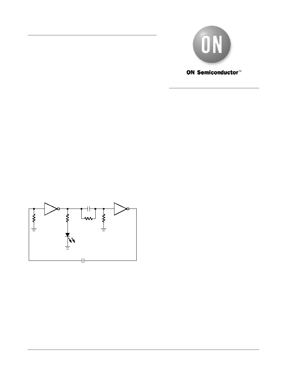
Figure 1. LED Oscillator Circuit
NL27WZ04
NL27WZ04
V
4
R
1
12 k
V
1
V
2
V
3
U
1A
U
1B
R
4
1 M
R
3
39
R
2
12 k
C
2
0.01
µ
F
C
1
0.1
µ
F
LED
D
1
The versatile features of the two gate devices will be
demonstrated by using the NL27WZ04 dual inverter IC to
create the Light Emitting Diode (LED) oscillator circuit
shown in Figure 1. An oscillator can be used to increase the
brightness of an LED without increasing the system's power
requirements. The brightness of an LED is directly
proportional to the current through the LED, which creates
a challenge for low voltage and battery powered
applications. Thus, a high peak current is required to obtain
a bright LED, while a low average current is needed to
minimize the power consumption. The LED oscillator
circuit achieves these requirements by providing a low duty
cycle waveform with a short duration "ON" time and a long
"OFF" time.
Light Emitting Diodes
LEDs are manufactured out of a variety of semiconductor
materials and are comprised of a "P" and "N" type junction,
which establishes a voltage potential across the junction.
The LED provides a light output when the diode is forward
biased, causing current to flow through the device. The
forward voltage (V
f
) of the diode will be different for the
various materials and colors and ranges from approximately
1.5 V for red to 3.3 V for blue LEDs.
A pulsating LED drive circuit can enhance the light output
of an LED by using a peak current of a much higher level
than sustainable under direct drive conditions [1][2]. A high
peak current pulse of short duration with a "OFF" period
between pulses allows time for the LED's junction to cool
down. High drive currents can result in a degradation of the
light output and the life expectancy (time to half light output)
of an LED. However, the reduction in the life of a pulsed
LED is minimal if the peak current is below the maximum
current limit specified for the device.
Why Are Pulsed LEDs Brighter Than DC LEDs?
There are two main reasons why LEDs are brighter when
pulsed. First, the human eye functions as both a peak
detector and an integrator; therefore, the eye perceives a
pulsed LED's brightness somewhere between the peak and
the average brightness [4]. Thus, an LED driven by a high
intensity low duty cycle light looks brighter in a pulsed
circuit compared to a DC drive circuit that is equal to the
average of the pulsed signal.
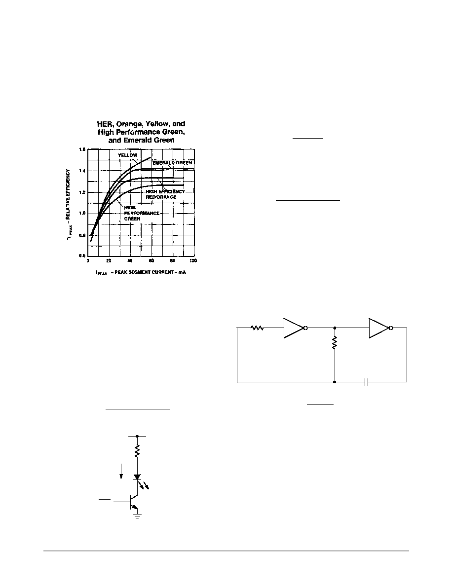
The second factor controlling the improved brightness is
shown in the relative efficiency versus peak current curves
of an LED. Figure 2 shows the efficiency curves for the
http://onsemi.com
APPLICATION NOTE
AND8067/D
http://onsemi.com
2
Agilent Technologies HLMP subminiature LED lamps [3].
For example, the pulsed emerald green LED will have a light
output approximately 30% brighter then the equivalent DC
drive circuit at a peak pulsed current of 30 mA. Note that the
pulsed circuit does not always produce a brighter LED. The
pulsed emerald green LED has a brighter light output at peak
currents greater than 10 mA; however, the DC circuit
produces a brighter LED for peak currents less than 10 mA.
Figure 2. LED Efficiency ≠ Pulsed vs. DC Operation
LED Drive Techniques
DC Method
Single LEDs are often driven using either a high side or
low side switch. The conventional LED interface circuit
consists of an open collector/drain driver to sink the LED
current as shown in Figure 3. The brightness of the LED is
proportional to the current (I
f
) through the diode. The
current through the LED for a current sinking configuration
is calculated using V
CC
, V
f
, R, and the voltage drop across
the driver (V
Switch
) as shown below.
If
+
VCC
*
Vf
*
VSwitch
R
Figure 3. Conventional Open Collector DC LED Circuit
V
CC
R
LED
ON/OFF
I
f
AC Method
The second method to drive LEDs uses a pulsating square
wave voltage. The suggested frequency and duty cycle
varies for different LEDs; however, the typical frequency
used is 1 kHz with a 10 to 30% duty cycle. Pulsing LEDs is
the standard method used with multiplexed displays when a
single driver circuit is interfaced to multiple LEDs. The
current through a pulsed current sourcing driver such as the
oscillator circuit shown in Figure 1 is calculated as shown
below.
If
+
VOH
*
Vf
R
Duty Cycle
(current sourcing driver)
The equation for a current sinking AC driver is similar to
the DC method, except that the duty cycle is used to reduce
the current consumption.
If
+
VCC
*
Vf
*
VSwitch
R
Duty Cycle
(current sinking driver)
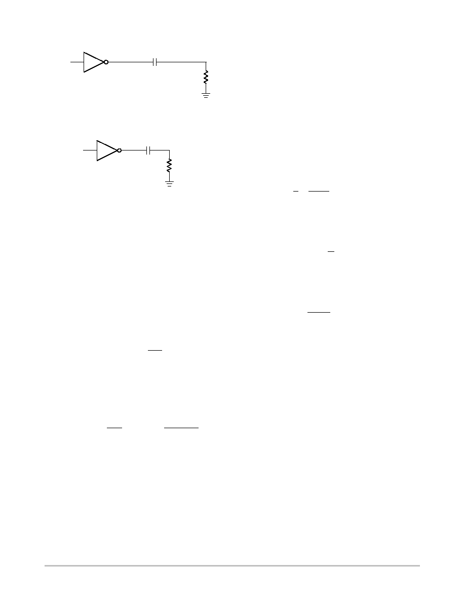
Dual Gate Inverter Oscillator Circuit
The LED oscillator circuit, shown in Figure 1 is derived
from the conventional two≠inverter oscillator shown in
Figure 4. The conventional oscillator is often denoted as an
astable multivibrator and has a duty cycle of approximately
50%. In contrast, the LED oscillator circuit has two RC time
constants so that both the duty cycle and frequency can be
adjusted. R
2
and C
2
control the "ON" time of the LED pulse,
while R
1
and C
1
control the "OFF" time.
Figure 4. Conventional Inverter Oscillator
U
1A
U
1B
R
1
C
1
R
2
fOscillation
^
1
2.3R1C1
(R2
+
10R1)
The LED oscillator with the NL27WZ04 duel gate
inverter and the given RC values is stable and does not have
the oscillation start≠up problem that often occurs with the
conventional two inverter oscillator. In order to ensure
oscillation at power≠up, R
4
was added in parallel with C
2
to
provide a DC path through the capacitor. The parallel
impedance combination of R
4
and C
2
is effectively equal to
the impedance of C
2
at the oscillation frequency; therefore,
R
4
does not effect the oscillation frequency.
The NL27WZ04 dual inverter is a standard buffered
inverter that produces either a "high" (i.e. V
cc
) or a "low"

AND8067/D
http://onsemi.com
3
(i.e. Ground) output voltage. In contrast, an unbuffered
inverter such as the NL27WZU04 functions as a voltage
amplifier for a small input voltage and thus can provide a
sine wave output during the oscillation start≠up period. It is
recommended that higher frequency oscillator applications,
such as a clock generation circuit, use the unbuffered
inverters.
The LED oscillator circuit shown in Figure 1 can be used
as a "Power ON" indicator. If NAND gates are used instead
of the inverters, ON/OFF control can be implemented for
applications such as status indicator lamps. This oscillator
circuit, shown in Figure 5, could be constructed using ON
Semiconductor's One≠Gate Logic family NAND devices.
The MC74VHC1G00 is the 2≠input NAND and the
MC74VHC1G01 is the 2≠input NAND with an open drain
output.
Figure 5. LED Oscillator Circuit with ON/OFF Control
R
1
U
1
R
4
R
3
C
2
C
1
LED
U
2
ON/OFF
R
2
V
CC
V
CC
Figure 6 shows V
1
, the LED drive voltage of the output of
inverter U
1A
. The input voltage V
2
to inverter U
1B
is shown
in Figure 7. Note that the voltage at V
2
may ring above V
CC
and below ground for a short duration because of capacitor
C
2
. The NL27WZ04 dual inverter has an absolute DC input
voltage rating of ≠0.5 V to 7 V. The maximum ratings are
specified at a steady state condition and the RMS value of the
high and low sides of the V
2
are within the input voltage
specification. The voltage at V
2
swings below ground;
however, the RMS value of the minimum voltage level is
equal to only approximately ≠50 mV.
Figure 6. V
1
, Output Voltage of Inverter U
1A
(V
CC
= 3.3 V)
0
V
oltage
(V)
≠0.5
Time (
µ
s)
0
0.5
1.5
2.0
2.5
3.0
3.5
500
1000
1500
2000
1.0
Figure 7. V
2
, Input Voltage of Inverter U
1B
(V
CC
= 3.3 V)
0
V
oltage
(V)
≠1.0
Time (
µ
s)
0
0.5
1.5
2.0
2.5
3.0
3.5
500
1000
1500
2000
1.0
≠0.5
Oscillation Equations for the Dual Inverter
Oscillator
The oscillation frequency and duty cycle of the oscillator
are obtained by analyzing the oscillator as two separate
circuits. The inverter subcircuits, shown in Figures 8 and 9,
are analyzed to obtain equations for the discharge times of
the RC networks formed at each inverter. In order to simplify
the calculation R
3
, R
4
and the LED will not be included in
the analysis. The error that results from neglecting these
components in the equations is small. In addition, the input
impedance of the inverter connected to the RC network can
be neglected because the input capacitance (C
IN
) for the
CMOS device is specified at only 2.5 pF.
AND8067/D
http://onsemi.com
4
Figure 8. "ON" Time Oscillator Subcircuit
U
1A
R
2
12 k
C
2
0.01
µ
F
V
4
V
1
V
2
Figure 9. "OFF" Time Oscillator Subcircuit
U
1B
R
1
12 k
C
1
0.1
µ
F
V
2
V
3
V
4
The equations are developed to predict the time it takes the
RC circuits to discharge to the threshold switching voltage
of the inverter. The threshold voltage of the inverters will be
assumed to be one≠half the supply voltage, which is equal
to the average of the High≠Level≠Input Voltage (V
IH
) and
the Low≠Level Input Voltage (V
IL
). The NL27WZ04
specifies V
IH
as 0.7
◊
V
CC
(minimum) and V
IL
as 0.3
◊
V
CC
(maximum). In addition, the initial voltage or the output
"High" voltage (V
OH
) of the inverter is assumed to be equal
to V
CC
. The actual V
OH
value is a function of the output
current and decreases as the output current increases.
The general equation for a RC circuit discharging to a
logic switching threshold voltage (V
th
) with an initial
voltage (V
i
) is as follows.
Vth
+
Vi
e
≠t
R
@
C
These assumptions result in the equation listed below that
can be solved for time (t).
Assume
Vth
+
0.5
V
and
Vi
+
VOH
^
VCC
Then
t
+ *
RC ln
Vth
VCC
+ *
RC ln
0.5
VCC
VCC
^
0.693
RC
LED "ON" Time
The LED's "ON" time is controlled by the discharge time
t
1
at inverter U
1A
, as shown from the equation listed below.
t1
^
0.693
R2C2
Substituting values into the equation yields:
t1
^
0.693
(12000
W
)(0.01
m
F)
^
83.2
m
s
LED "OFF" Time
The LED's "OFF" time is controlled by the discharge time
t
2
at inverter U
1B
, as shown from the equation listed below.
t2
^
0.693
R1C1
Substituting the values into the equation yields:
t2
^
0.693
(12000
W
)(0.1
m
F)
^
832
m
s
LED Oscillation Frequency
The time period (T) of the oscillator is equal to the sum of
the charge times in the first and second RC stages. Note the
propagation delay of the inverters can be ignored at the LED
circuit's oscillation frequency of 1 kHz.
T
+
t1
)
t2
T
+
83.2
m
s
)
832
m
s
+
915
m
s
f
+
1
T
+
1
915
m
s
+
1.09 kHz
LED Duty Cycle
The duty cycle (DS) for the oscillator at V
1
is given by the
equation:
DSV1
+
t1
t2
100%
The duty cycle of the oscillator is proportional to the ratio
of the two time constants that are set by capacitors C
1
and C
2
.
The LED oscillator has a duty cycle of ten percent as shown
below.
DSV1
+
83.2
m
s
832
m
s
100%
+
10%
Experimental Results
The operating characteristics of the pulsed LED oscillator
circuit were compared to the DC circuit shown in Figure 10.
The DC circuit's current limiting resistor R
5
was selected so
the current through the LED was equal to the average (RMS)
current of the oscillator circuit's LED. A high efficiency
green GaP/GaP LED from Chicago Miniature Lamp (part
number CMD64531) was used to evaluate the circuits. The
resistor and capacitor values are listed below.
Component Values
LED Oscillator Circuit (Figure 1):
R
1
= R
2
= 12 k
R
3
= 39
R
4
= 1 M
C1 = 0.1
µ
F
C2 = 0.01
µ
F
DC LED Circuit (Figure 10):
R
5
= 680
AND8067/D
http://onsemi.com
5
Figure 10. DC LED Circuit with Normalized Current
Equal to the Pulsed LED Oscillator of Figure 1
R
5
680
LED
D
2
V
CC
The oscillation and LED current measurements are
summarized in Table 1. Figure 11 shows the PCB that was
created to verify the operation of the LED circuits. The error
in the calculated versus measure oscillation frequency is a
result of the assumptions that V
OH
= V
CC
and V
TH
= 0.5
◊
V
CC
. In addition, the tolerance of the resistors and capacitors
contributed to the frequency error. The pulsed LED is
noticeably brighter than the DC LED; however, the LED's
light output was not quantified with a light spectrometer.
Note that the maximum average current limit of the
NL27WZ04 inverter is specified at 24 ma. The pulsed peak
current exceeds the maximum limit; however, the current
rating of the device is not exceeded because the average
current is below the 24 ma limit. Although a maximum peak
current limit is typically not specified for logic devices, a
safe peak current can be verified by measuring the case
temperature of the IC. If the temperature of the logic device
is significantly higher than the ambient (i.e. 10≠20
_C), the
reliability of the circuit maybe reduced. The case
temperature of the NL27WZ04 inverter of the LED
oscillator did not significantly increase.
Table 1. Experimental Results of the LED Oscillator
V
CC
Calculated
Oscillation
Frequency
Measured
Oscillation
Frequency
Measured
Duty Cycle
Pulsed LED
Peak Current
Pulsed LED
Average (RMS)
Current
DC LED
Average Current
2.5 V
1.09 kHz
1.24 kHz
9.4%
9.79 mA
0.92 mA
0.98 mA
3.3 V
1.09 kHz
1.11 kHz
9.4%
21.3 mA
2.00 mA
2.06 mA
5.0 V
1.09 kHz
1.04 kHz
9.4%
46.7 mA
4.39 mA
4.45 mA
Figure 11. LED Oscillator Evaluation PCB
BIBLIOGRAPHY
1. "Application Note 1005: Operational
Considerations for LED Lamps and Display
Devices," Agilent Technologies, 1999.
2. "Guidelines for Designs using LEDs: How to
Enhance Display Performance without Increasing
the Drive Current," Fairchild Semiconductor,
1999.
3. HLMP≠Pxxx, HLMP≠Qxxx, HLMP≠6xxx and
HLMP≠70xx Series Subminiature LED Lamps
Datasheet, Agilent Technologies, 2000.
4. Smith, George, "Multiplexing LED Displays:
Appnote 3," Siemens Semiconductor.

AND8067/D
http://onsemi.com
6
Notes

AND8067/D
http://onsemi.com
7
Notes

AND8067/D
http://onsemi.com
8
ON Semiconductor and are trademarks of Semiconductor Components Industries, LLC (SCILLC). SCILLC reserves the right to make changes
without further notice to any products herein. SCILLC makes no warranty, representation or guarantee regarding the suitability of its products for any particular
purpose, nor does SCILLC assume any liability arising out of the application or use of any product or circuit, and specifically disclaims any and all liability,
including without limitation special, consequential or incidental damages. "Typical" parameters which may be provided in SCILLC data sheets and/or
specifications can and do vary in different applications and actual performance may vary over time. All operating parameters, including "Typicals" must be
validated for each customer application by customer's technical experts. SCILLC does not convey any license under its patent rights nor the rights of others.
SCILLC products are not designed, intended, or authorized for use as components in systems intended for surgical implant into the body, or other applications
intended to support or sustain life, or for any other application in which the failure of the SCILLC product could create a situation where personal injury or
death may occur. Should Buyer purchase or use SCILLC products for any such unintended or unauthorized application, Buyer shall indemnify and hold
SCILLC and its officers, employees, subsidiaries, affiliates, and distributors harmless against all claims, costs, damages, and expenses, and reasonable
attorney fees arising out of, directly or indirectly, any claim of personal injury or death associated with such unintended or unauthorized use, even if such claim
alleges that SCILLC was negligent regarding the design or manufacture of the part. SCILLC is an Equal Opportunity/Affirmative Action Employer.
PUBLICATION ORDERING INFORMATION
JAPAN: ON Semiconductor, Japan Customer Focus Center
4≠32≠1 Nishi≠Gotanda, Shinagawa≠ku, Tokyo, Japan 141≠0031
Phone: 81≠3≠5740≠2700
Email: r14525@onsemi.com
ON Semiconductor Website: http://onsemi.com
For additional information, please contact your local
Sales Representative.
AND8067/D
Literature Fulfillment:
Literature Distribution Center for ON Semiconductor
P.O. Box 5163, Denver, Colorado 80217 USA
Phone: 303≠675≠2175 or 800≠344≠3860 Toll Free USA/Canada
Fax: 303≠675≠2176 or 800≠344≠3867 Toll Free USA/Canada
Email: ONlit@hibbertco.com
N. American Technical Support: 800≠282≠9855 Toll Free USA/Canada