 | ÐлекÑÑоннÑй компоненÑ: BC858CL | СкаÑаÑÑ:  PDF PDF  ZIP ZIP |
BC856ALT1
©
Semiconductor Components Industries, LLC, 2001
January, 2001 Rev. 2
Publication Order Number:
BC856ALT1/D
BC856ALT1 Series
Preferred Devices
General Purpose
Transistors
PNP Silicon
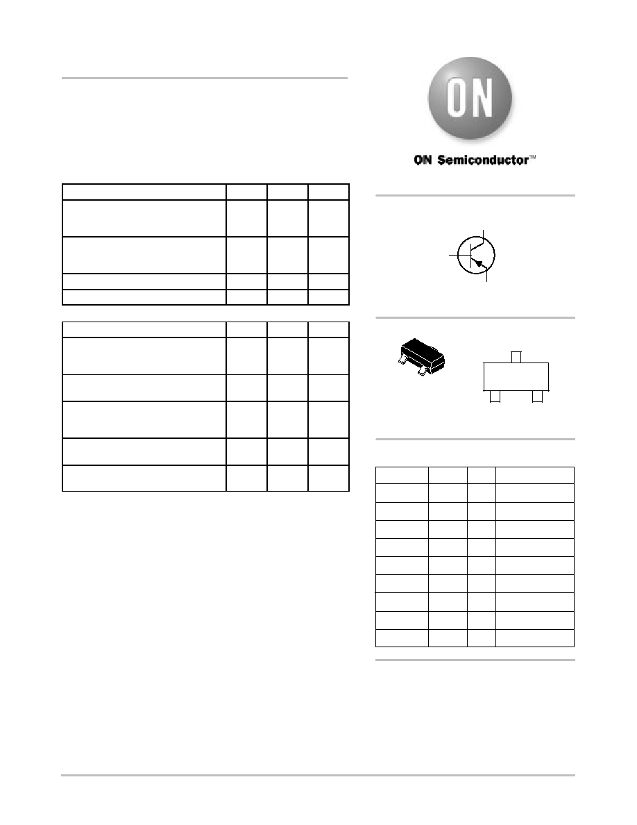
MAXIMUM RATINGS
(T
A
= 25
°
C unless otherwise noted)
Rating
Symbol
Value
Unit
Collector-Emitter Voltage
BC856
BC857
BC858, BC859
V
CEO
65
45
30
V
Collector-Base Voltage
BC856
BC857
BC858, BC859
V
CBO
80
50
30
V
EmitterBase Voltage
V
EBO
5.0
V
Collector Current Continuous
I
C
100
mAdc
THERMAL CHARACTERISTICS
Characteristic
Symbol
Max
Unit
Total Device Dissipation FR5 Board,
(Note 1.) T
A
= 25
°
C
Derate above 25
°
C
P
D
225
1.8
mW
mW/
°
C
Thermal Resistance,
Junction to Ambient
R
q
JA
556
°
C/W
Total Device Dissipation Alumina
Substrate, (Note 2.) T
A
= 25
°
C
Derate above 25
°
C
P
D
300
2.4
mW
mW/
°
C
Thermal Resistance,
Junction to Ambient
R
q
JA
417
°
C/W
Junction and Storage Temperature
T
J
, T
stg
55 to
+150
°
C
1. FR5 = 1.0 x 0.75 x 0.062 in
2. Alumina = 0.4 x 0.3 x 0.024 in. 99.5% alumina.
http://onsemi.com
SOT23
CASE 318
STYLE 6
MARKING DIAGRAM
xx
= Device Code
=
(See Table Below)
1
2
3
1
2
3
xx
Preferred devices are recommended choices for future use
and best overall value.
COLLECTOR
3
1
BASE
2
EMITTER
Device
Package
Shipping
ORDERING INFORMATION
BC856ALT1 SOT23
3000/Tape & Reel
BC856BLT1
SOT23
3000/Tape & Reel
BC857ALT1 SOT23
3000/Tape & Reel
BC857BLT1
SOT23
3000/Tape & Reel
BC858ALT1 SOT23
3000/Tape & Reel
BC858BLT1
SOT23
3000/Tape & Reel
BC858CLT1 SOT23
3000/Tape & Reel
BC859BLT1
SOT23
3000/Tape & Reel
BC859CLT1
SOT23
3000/Tape & Reel
Mark
3A
3B
3E
3F
3J
3K
3L
4B
4C

BC856ALT1 Series
http://onsemi.com
2
ELECTRICAL CHARACTERISTICS
(T
A
= 25
°
C unless otherwise noted)
Characteristic
Symbol
Min
Typ
Max
Unit
OFF CHARACTERISTICS
CollectorEmitter Breakdown Voltage
BC856 Series
(I
C
= 10 mA)
BC857 Series
BC858, BC859 Series
V
(BR)CEO
65
45
30
V
CollectorEmitter Breakdown Voltage
BC856 Series
(I
C
= 10
µ
A, V
EB
= 0)
BC857 Series
BC858, BC859 Series
V
(BR)CES
80
50
30
V
CollectorBase Breakdown Voltage
BC856 Series
(I
C
= 10
m
A)
BC857 Series
BC858, BC859 Series
V
(BR)CBO
80
50
30
V
EmitterBase Breakdown Voltage
BC856 Series
(I
E
= 1.0
m
A)
BC857 Series
BC858, BC859 Series
V
(BR)EBO
5.0
5.0
5.0
V
Collector Cutoff Current (V
CB
= 30 V)
Collector Cutoff Current
(V
CB
= 30 V, T
A
= 150
°
C)
I
CBO
15
4.0
nA
µ
A
ON CHARACTERISTICS
DC Current Gain
BC856A, BC857A, BC858A
(I
C
= 10
µ
A, V
CE
= 5.0 V)
BC856B, BC857B, BC858B
BC858C
(I
C
= 2.0 mA, V
CE
= 5.0 V)
BC856A, BC857A, BC858A
BC856B, BC857B, BC858B, BC859B
BC858C, BC859C
h
FE
125
220
420
90
150
270
180
290
520
250
475
800
CollectorEmitter Saturation Voltage
(I
C
= 10 mA, I
B
= 0.5 mA)
(I
C
= 100 mA, I
B
= 5.0 mA)
V
CE(sat)
0.3
0.65
V
BaseEmitter Saturation Voltage
(I
C
= 10 mA, I
B
= 0.5 mA)
(I
C
= 100 mA, I
B
= 5.0 mA)
V
BE(sat)
0.7
0.9
V
BaseEmitter On Voltage
(I
C
= 2.0 mA, V
CE
= 5.0 V)
(I
C
= 10 mA, V
CE
= 5.0 V)
V
BE(on)
0.6
0.75
0.82
V
SMALLSIGNAL CHARACTERISTICS
CurrentGain Bandwidth Product
(I
C
= 10 mA, V
CE
= 5.0 Vdc, f = 100 MHz)
f
T
100
MHz
Output Capacitance
(V
CB
= 10 V, f = 1.0 MHz)
C
ob
4.5
pF
Noise Figure
(I
C
= 0.2 mA, V
CE
= 5.0 Vdc, R
S
= 2.0 k
, f = 1.0 kHz, BW = 200 Hz)
BC856, BC857, BC858 Series
BC859 Series
NF
10
4.0
dB
BC856ALT1 Series
http://onsemi.com
3
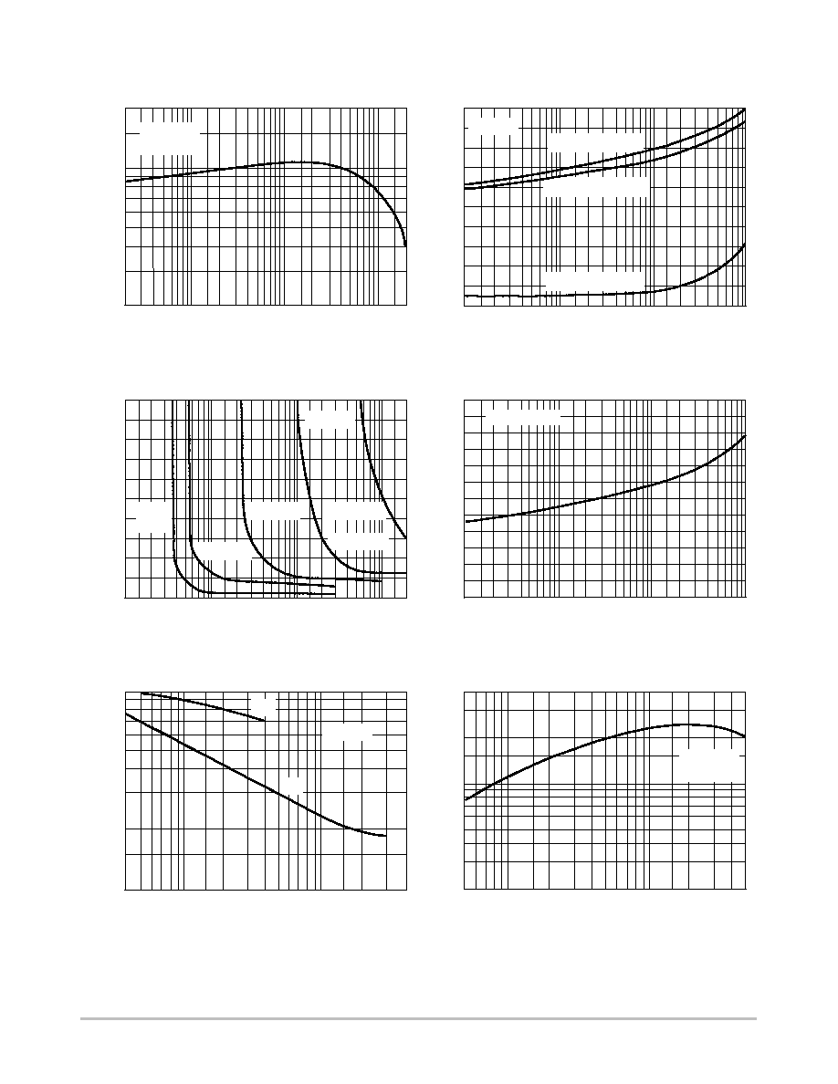
BC857/BC858/BC859
Figure 1. Normalized DC Current Gain
I
C
, COLLECTOR CURRENT (mAdc)
2.0
Figure 2. "Saturation" and "On" Voltages
I
C
, COLLECTOR CURRENT (mAdc)
-0.2
0.2
Figure 3. Collector Saturation Region
I
B
, BASE CURRENT (mA)
Figure 4. BaseEmitter Temperature Coefficient
I
C
, COLLECTOR CURRENT (mA)
-0.6
-0.7
-0.8
-0.9
-1.0
-0.5
0
-0.2
-0.4
-0.1
-0.3
1.6
1.2
2.0
2.8
2.4
-1.2
-1.6
-2.0
-0.02
-1.0
-10
0
-20
-0.1
-0.4
-0.8
h FE
, NORMALIZED DC CURRENT
GAIN
V
,
VOL
T
AGE (VOL
TS)
V CE
, COLLECT
OR-EMITTER VOL
T
AGE (V)
VB
,
TEMPERA
TURE COEFFICIENT
(mV/
C)
°
1.5
1.0
0.7
0.5
0.3
-0.2
-10
-100
-1.0
T
A
= 25
°
C
V
BE(sat)
@ I
C
/I
B
= 10
V
CE(sat)
@ I
C
/I
B
= 10
V
BE(on)
@ V
CE
= -10 V
V
CE
= -10 V
T
A
= 25
°
C
-55
°
C to +125
°
C
I
C
= -100 mA
I
C
= -20 mA
-0.5 -1.0 -2.0
-5.0 -10 -20
-50 -100 -200
-0.1 -0.2
-0.5 -1.0 -2.0
-5.0 -10 -20
-50 -100
I
C
= -200 mA
I
C
= -50 mA
I
C
=
-10 mA
Figure 5. Capacitances
V
R
, REVERSE VOLTAGE (VOLTS)
10
Figure 6. CurrentGain Bandwidth Product
I
C
, COLLECTOR CURRENT (mAdc)
-0.4
1.0
80
100
200
300
400
60
20
40
30
7.0
5.0
3.0
2.0
-0.5
C, CAP
ACIT
ANCE (pF)
f, CURRENT-GAIN - BANDWIDTH PRODUCT
(MHz)
T
T
A
= 25
°
C
C
ob
C
ib
-0.6
-1.0
-2.0
-4.0 -6.0
-10
-20 -30 -40
150
-1.0
-2.0 -3.0 -5.0
-10
-20 -30 -50
V
CE
= -10 V
T
A
= 25
°
C
T
A
= 25
°
C
1.0
BC856ALT1 Series
http://onsemi.com
4
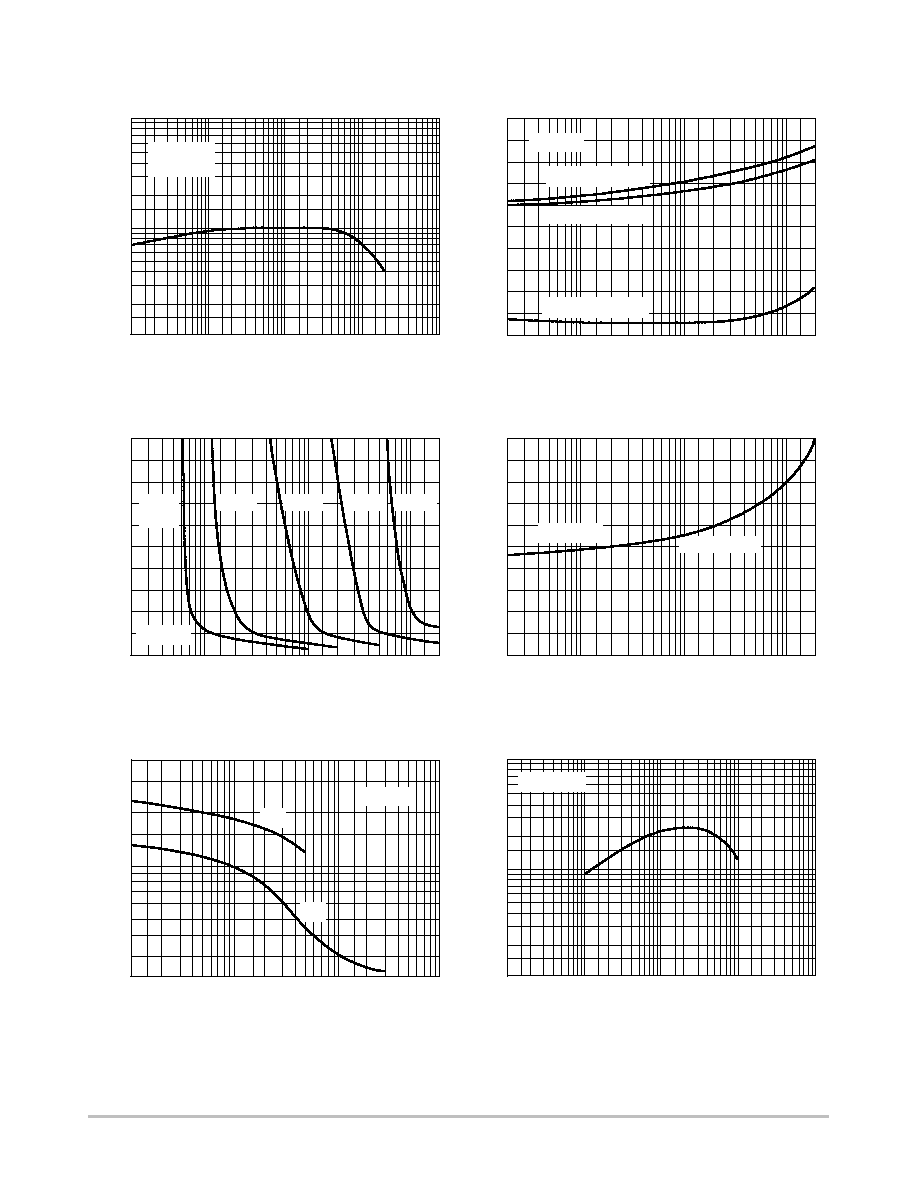
BC856
Figure 7. DC Current Gain
I
C
, COLLECTOR CURRENT (AMP)
Figure 8. "On" Voltage
I
C
, COLLECTOR CURRENT (mA)
-0.8
-1.0
-0.6
-0.2
-0.4
1.0
2.0
-0.1
-1.0
-10
-200
-0.2
0.2
0.5
-0.2
-1.0
-10
-200
T
J
= 25
°
C
V
BE(sat)
@ I
C
/I
B
= 10
V
CE(sat)
@ I
C
/I
B
= 10
V
BE
@ V
CE
= -5.0 V
Figure 9. Collector Saturation Region
I
B
, BASE CURRENT (mA)
Figure 10. BaseEmitter Temperature Coefficient
I
C
, COLLECTOR CURRENT (mA)
-1.0
-1.2
-1.6
-2.0
-0.02
-1.0
-10
0
-20
-0.1
-0.4
-0.8
V CE
, COLLECT
OR-EMITTER VOL
T
AGE (VOL
TS)
VB
,
TEMPERA
TURE COEFFICIENT
(mV/
C)
°
-0.2
-2.0
-10
-200
-1.0
T
J
= 25
°
C
I
C
=
-10 mA
h FE
, DC CURRENT
GAIN (NORMALIZED)
V
,
VOL
T
AGE (VOL
TS)
V
CE
= -5.0 V
T
A
= 25
°
C
0
-0.5
-2.0
-5.0
-20
-50 -100
-0.05
-0.2
-0.5
-2.0
-5.0
-100 mA
-20 mA
-1.4
-1.8
-2.2
-2.6
-3.0
-0.5
-5.0
-20
-50 -100
-55
°
C to 125
°
C
VB
for V
BE
-2.0 -5.0
-20 -50 -100
Figure 11. Capacitance
V
R
, REVERSE VOLTAGE (VOLTS)
40
Figure 12. CurrentGain Bandwidth Product
I
C
, COLLECTOR CURRENT (mA)
-0.1 -0.2
-1.0
-50
2.0
-2.0
-10
-100
100
200
500
50
20
20
10
6.0
4.0
-1.0
-10
-100
V
CE
= -5.0 V
C, CAP
ACIT
ANCE (pF)
f, CURRENT-GAIN - BANDWIDTH PRODUCT T
-0.5
-5.0
-20
T
J
= 25
°
C
C
ob
C
ib
8.0
-50 mA
-200 mA
BC856ALT1 Series
http://onsemi.com
5
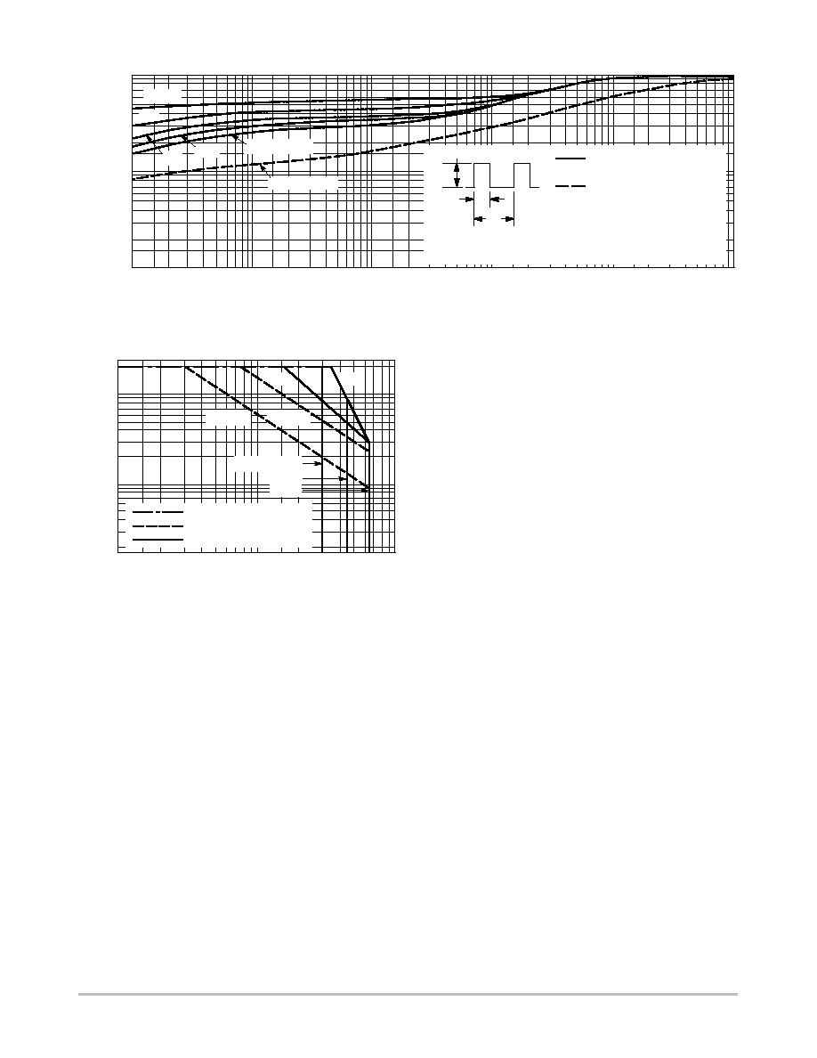
Figure 13. Thermal Response
t, TIME (ms)
1.0
r(t), TRANSIENT
THERMAL
2.0
5.0
1.0
0.5
0.2
0.1
RESIST
ANCE (NORMALIZED)
0.7
0.5
0.3
0.2
0.1
0.07
0.05
0.03
0.02
0.01
20
50
10
200
500
100
1.0 k
2.0 k
5.0 k 10 k
Figure 14. Active Region Safe Operating Area
V
CE
, COLLECTOR-EMITTER VOLTAGE (V)
-200
-1.0
I C
, COLLECT
OR CURRENT
(mA)
T
A
= 25
°
C
D = 0.5
0.2
0.1
0.05
SINGLE PULSE
SINGLE PULSE
BONDING WIRE LIMIT
THERMAL LIMIT
SECOND BREAKDOWN LIMIT
3 ms
T
J
= 25
°
C
Z
JC
(t) = r(t) R
JC
R
JC
= 83.3
°
C/W MAX
Z
JA
(t) = r(t) R
JA
R
JA
= 200
°
C/W MAX
D CURVES APPLY FOR POWER
PULSE TRAIN SHOWN
READ TIME AT t
1
T
J(pk)
- T
C
= P
(pk)
R
JC
(t)
t
1
t
2
P
(pk)
DUTY CYCLE, D = t
1
/t
2
-100
-50
-10
-5.0
-2.0
-5.0
-10
-30 -45 -65 -100
1 s
BC558, BC559
BC557
BC556
The safe operating area curves indicate I
C
V
CE
limits of
the transistor that must be observed for reliable operation.
Collector load lines for specific circuits must fall below the
limits indicated by the applicable curve.
The data of Figure 14 is based upon T
J(pk)
= 150
°
C; T
C
or
T
A
is variable depending upon conditions. Pulse curves are
valid for duty cycles to 10% provided T
J(pk)
150
°
C. T
J(pk)
may be calculated from the data in Figure 13. At high case or
ambient temperatures, thermal limitations will reduce the
power that can be handled to values less than the limitations
imposed by the secondary breakdown.