 | –≠–ª–µ–∫—Ç—Ä–æ–Ω–Ω—ã–π –∫–æ–º–ø–æ–Ω–µ–Ω—Ç: BD682T | –°–∫–∞—á–∞—Ç—å:  PDF PDF  ZIP ZIP |
©
Semiconductor Components Industries, LLC, 2002
April, 2002 ≠ Rev. 10
Publication Order Number:
BD676/D
BD676, BD676A, BD678,
BD678A, BD680, BD680A,
BD682
Plastic Medium-Power
Silicon PNP Darlingtons
...for use as output devices in complementary general≠purpose
amplifier applications.
∑
High DC Current Gain ≠
hFE = 750 (Min) @ IC = 1.5 and 2.0 Adc
∑
Monolithic Construction
∑
BD676, 676A, 678, 678A, 680, 680A, 682 are complementary with
BD675, 675A, 677, 677A, 679, 679A, 681
∑
BD 678, 678A, 680, 680A are equivalent to MJE 700, 701, 702, 703
MAXIMUM RATINGS
Rating
Symbol
Value
Unit
Collector-Emitter Voltage
BD676, BD676A
BD678, BD678A
BD680, BD680A
BD682
VCEO
45
60
80
100
Vdc
Collector-Base Voltage
BD676, BD676A
BD678, BD678A
BD680, BD680A
BD682
VCB
45
60
80
100
Vdc
Emitter-Base Voltage
VEB
5.0
Vdc
Collector Current
IC
4.0
Adc
Base Current
IB
0.1
Adc
Total Device Dissipation
@ TC = 25
∞
C
Derate above 25
∞
C
PD
40
0.32
W
W/
∞
C
Operating and Storage Junction
Temperature Range
TJ, Tstg
≠55 to +150
∞
C
THERMAL CHARACTERISTICS
Characteristic
Symbol
Max
Unit
Thermal Resistance ≠
Junction to Case
R
JC
3.13
∞
C/W
TO≠225AA
CASE 77
STYLE 1
MARKING DIAGRAM
Y
= Year
WW
= Work Week
BD6xxx = Specific Device Code
xxx
= 76, 76A, 78, 78A, 80, 80A or 82
Device
Package
Shipping
ORDERING INFORMATION
BD676
TO≠225AA
500 Units/Box
4.0 AMPERE
DARLINGTON
POWER TRANSISTORS
PNP SILICON
45, 60, 80, 100 VOLTS
40 WATTS
BD676A
TO≠225AA
500 Units/Box
BD678
TO≠225AA
500 Units/Box
BD678A
TO≠225AA
500 Units/Box
BD680
TO≠225AA
500 Units/Box
BD680A
TO≠225AA
500 Units/Box
BD682
TO≠225AA
500 Units/Box
YWW
BD6xxx
3
2 1
STYLE 1:
PIN 1. EMITTER
2. COLLECTOR
3. BASE
http://onsemi.com
BD676, BD676A, BD678, BD678A, BD680, BD680A, BD682
http://onsemi.com
2
ŒŒŒŒŒŒŒŒŒŒŒŒŒŒŒŒŒŒŒŒŒŒŒŒŒŒŒŒŒŒŒŒŒ
ŒŒŒŒŒŒŒŒŒŒŒŒŒŒŒŒŒŒŒŒŒŒŒŒŒŒŒŒŒŒŒŒŒ
ELECTRICAL CHARACTERISTICS
(TC = 25
_
C unless otherwise noted)
ŒŒŒŒŒŒŒŒŒŒŒŒŒŒŒŒŒŒŒŒŒŒ
ŒŒŒŒŒŒŒŒŒŒŒŒŒŒŒŒŒŒŒŒŒŒ
Characteristic
ŒŒŒŒ
ŒŒŒŒ
Symbol
ŒŒŒŒ
ŒŒŒŒ
Min
ŒŒŒŒ
ŒŒŒŒ
Max
ŒŒŒ
ŒŒŒ
Unit
ŒŒŒŒŒŒŒŒŒŒŒŒŒŒŒŒŒŒŒŒŒŒŒŒŒŒŒŒŒŒŒŒŒ
ŒŒŒŒŒŒŒŒŒŒŒŒŒŒŒŒŒŒŒŒŒŒŒŒŒŒŒŒŒŒŒŒŒ
OFF CHARACTERISTICS
ŒŒŒŒŒŒŒŒŒŒŒŒŒŒŒŒŒŒŒŒŒŒ
Œ
ŒŒŒŒŒŒŒŒŒŒŒŒŒŒŒŒŒŒŒŒ
Œ
Œ
ŒŒŒŒŒŒŒŒŒŒŒŒŒŒŒŒŒŒŒŒ
Œ
ŒŒŒŒŒŒŒŒŒŒŒŒŒŒŒŒŒŒŒŒŒŒ
Collector≠Emitter Breakdown Voltage (Note 1)
BD676, 676A
(IC = 50 mAdc, IB = 0)
BD678, 678A
BD680, 680A
BD682
ŒŒŒŒ
Œ
ŒŒ
Œ
Œ
ŒŒ
Œ
ŒŒŒŒ
BVCEO
ŒŒŒŒ
Œ
ŒŒ
Œ
Œ
ŒŒ
Œ
ŒŒŒŒ
45
60
80
100
ŒŒŒŒ
Œ
ŒŒ
Œ
Œ
ŒŒ
Œ
ŒŒŒŒ
≠
≠
≠
≠
ŒŒŒ
Œ
Œ
Œ
Œ
Œ
Œ
ŒŒŒ
Vdc
ŒŒŒŒŒŒŒŒŒŒŒŒŒŒŒŒŒŒŒŒŒŒ
ŒŒŒŒŒŒŒŒŒŒŒŒŒŒŒŒŒŒŒŒŒŒ
Collector Cutoff Current (VCE = Half Rated VCEO, IB = 0)
ŒŒŒŒ
ŒŒŒŒ
ICEO
ŒŒŒŒ
ŒŒŒŒ
≠
ŒŒŒŒ
ŒŒŒŒ
500
ŒŒŒ
ŒŒŒ
µ
Adc
ŒŒŒŒŒŒŒŒŒŒŒŒŒŒŒŒŒŒŒŒŒŒ
Œ
ŒŒŒŒŒŒŒŒŒŒŒŒŒŒŒŒŒŒŒŒ
Œ
ŒŒŒŒŒŒŒŒŒŒŒŒŒŒŒŒŒŒŒŒŒŒ
Collector Cutoff Current
(VCB = Rated BVCEO, IE = 0)
(VCB = Rated BVCEO. IE = 0, TC = 100
∞
C)
ŒŒŒŒ
Œ
ŒŒ
Œ
ŒŒŒŒ
ICBO
ŒŒŒŒ
Œ
ŒŒ
Œ
ŒŒŒŒ
≠
≠
ŒŒŒŒ
Œ
ŒŒ
Œ
ŒŒŒŒ
0.2
2.0
ŒŒŒ
Œ
Œ
Œ
ŒŒŒ
mAdc
ŒŒŒŒŒŒŒŒŒŒŒŒŒŒŒŒŒŒŒŒŒŒ
ŒŒŒŒŒŒŒŒŒŒŒŒŒŒŒŒŒŒŒŒŒŒ
Emitter Cutoff Current (VBE = 5.0 Vdc, IC = 0)
ŒŒŒŒ
ŒŒŒŒ
IEBO
ŒŒŒŒ
ŒŒŒŒ
≠
ŒŒŒŒ
ŒŒŒŒ
2.0
ŒŒŒ
ŒŒŒ
mAdc
ŒŒŒŒŒŒŒŒŒŒŒŒŒŒŒŒŒŒŒŒŒŒŒŒŒŒŒŒŒŒŒŒŒ
ŒŒŒŒŒŒŒŒŒŒŒŒŒŒŒŒŒŒŒŒŒŒŒŒŒŒŒŒŒŒŒŒŒ
ON CHARACTERISTICS
ŒŒŒŒŒŒŒŒŒŒŒŒŒŒŒŒŒŒŒŒŒŒ
Œ
ŒŒŒŒŒŒŒŒŒŒŒŒŒŒŒŒŒŒŒŒ
Œ
ŒŒŒŒŒŒŒŒŒŒŒŒŒŒŒŒŒŒŒŒŒŒ
DC Current Gain (Note 1)
(IC = 1.5 Adc, VCE = 3.0 Vdc)
BD676, 678, 680, 682
(IC = 2.0 Adc, VCE = 3.0 Vdc)
BD676A, 678A, 680A
ŒŒŒŒ
Œ
ŒŒ
Œ
ŒŒŒŒ
hFE
ŒŒŒŒ
Œ
ŒŒ
Œ
ŒŒŒŒ
750
750
ŒŒŒŒ
Œ
ŒŒ
Œ
ŒŒŒŒ
≠
≠
ŒŒŒ
Œ
Œ
Œ
ŒŒŒ
ŒŒŒŒŒŒŒŒŒŒŒŒŒŒŒŒŒŒŒŒŒŒ
Œ
ŒŒŒŒŒŒŒŒŒŒŒŒŒŒŒŒŒŒŒŒ
Œ
Œ
ŒŒŒŒŒŒŒŒŒŒŒŒŒŒŒŒŒŒŒŒ
Œ
ŒŒŒŒŒŒŒŒŒŒŒŒŒŒŒŒŒŒŒŒŒŒ
Collector≠Emitter Saturation Voltage (Note 1)
(IC = 1.5 Adc, IB = 30 mAdc)
BD678, 680, 682
(IC = 2.0 Adc, IB = 40 mAdc)
BD676A, 678A, 680A
ŒŒŒŒ
Œ
ŒŒ
Œ
Œ
ŒŒ
Œ
ŒŒŒŒ
VCE(sat)
ŒŒŒŒ
Œ
ŒŒ
Œ
Œ
ŒŒ
Œ
ŒŒŒŒ
≠
≠
ŒŒŒŒ
Œ
ŒŒ
Œ
Œ
ŒŒ
Œ
ŒŒŒŒ
2.5
2.8
ŒŒŒ
Œ
Œ
Œ
Œ
Œ
Œ
ŒŒŒ
Vdc
ŒŒŒŒŒŒŒŒŒŒŒŒŒŒŒŒŒŒŒŒŒŒ
Œ
ŒŒŒŒŒŒŒŒŒŒŒŒŒŒŒŒŒŒŒŒ
Œ
ŒŒŒŒŒŒŒŒŒŒŒŒŒŒŒŒŒŒŒŒŒŒ
Base≠Emitter On Voltage (Note 1)
(IC = 1.5 Adc, VCE = 3.0 Vdc)
BD678, 680, 682
(IC = 2.0 Adc, VCE = 3.0 Vdc)
BD676A, 678A, 680A
ŒŒŒŒ
Œ
ŒŒ
Œ
ŒŒŒŒ
VBE(on)
ŒŒŒŒ
Œ
ŒŒ
Œ
ŒŒŒŒ
≠
≠
ŒŒŒŒ
Œ
ŒŒ
Œ
ŒŒŒŒ
2.5
2.5
ŒŒŒ
Œ
Œ
Œ
ŒŒŒ
Vdc
ŒŒŒŒŒŒŒŒŒŒŒŒŒŒŒŒŒŒŒŒŒŒŒŒŒŒŒŒŒŒŒŒŒ
ŒŒŒŒŒŒŒŒŒŒŒŒŒŒŒŒŒŒŒŒŒŒŒŒŒŒŒŒŒŒŒŒŒ
DYNAMIC CHARACTERISTICS
ŒŒŒŒŒŒŒŒŒŒŒŒŒŒŒŒŒŒŒŒŒŒ
ŒŒŒŒŒŒŒŒŒŒŒŒŒŒŒŒŒŒŒŒŒŒ
Small≠Signal Current Gain (IC = 1.5 Adc, VCE = 3.0 Vdc, f = 1.0 MHz)
ŒŒŒŒ
ŒŒŒŒ
hfe
ŒŒŒŒ
ŒŒŒŒ
1.0
ŒŒŒŒ
ŒŒŒŒ
≠
ŒŒŒ
ŒŒŒ
≠
1. Pulse Test: Pulse Width
v
300
µ
s, Duty Cycle
v
2.0%.
50
40
10
5.0
0
15
30
45
60
75
105
135 150 165
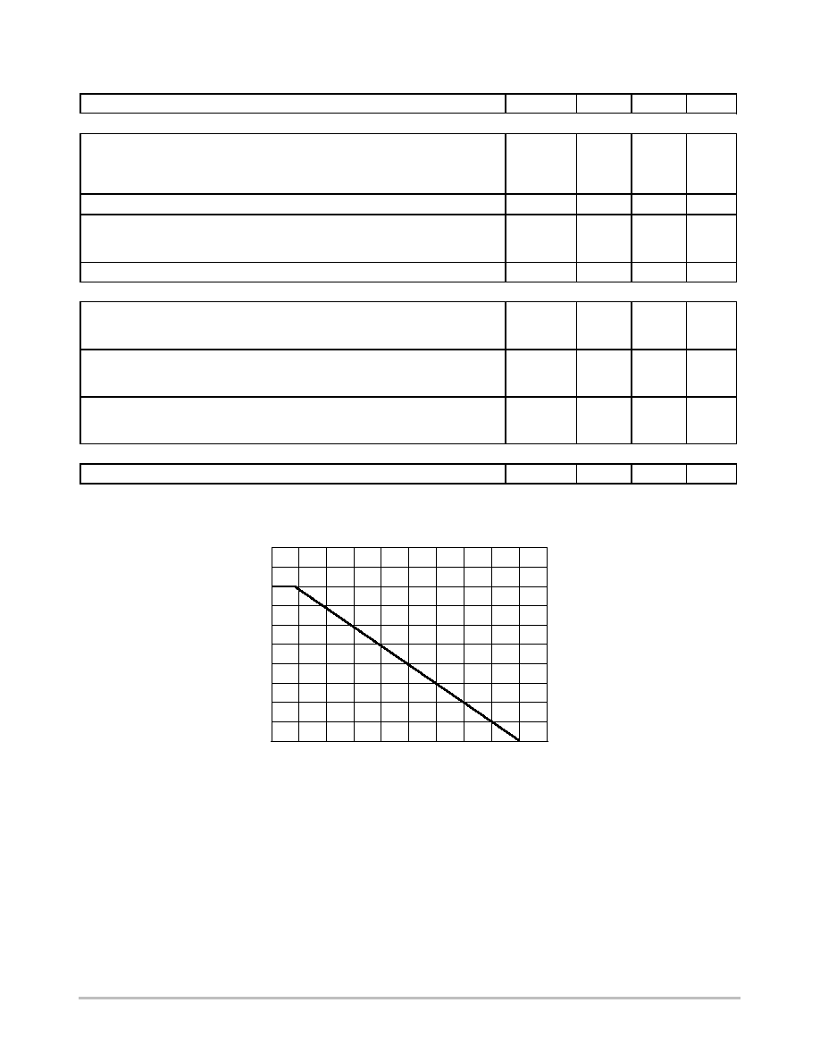
Figure 1. Power Temperature Derating
TC, CASE TEMPERATURE (
∞
C)
P D
, POWER DISSIP
A
TION (W
A
TTS)
120
90
45
20
15
30
25
35
BD676, BD676A, BD678, BD678A, BD680, BD680A, BD682
http://onsemi.com
3
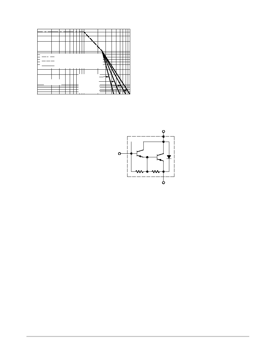
Figure 2. DC Safe Operating Area
5.0
1.0
VCE, COLLECTOR-EMITTER VOLTAGE (VOLTS)
2.0
1.0
0.5
0.05
2.0
5.0
10
50
100
BONDING WIRE LIMIT
THERMAL LIMIT at TC = 25
∞
C
SECONDARY BREAKDOWN LIMIT
0.2
0.1
I C
, COLLECT
OR CURRENT
(AMP)
TC = 25
∞
C
BD676, 676A
BD678, 678A
BD680, 680A
BD682
20
There are two limitations on the power handling ability of
a transistor average junction temperature and secondary
breakdown. Safe operating area curves indicate IC ≠ VCE
limits of the transistor that must be observed for reliable
operation; e.g., the transistor must not be subjected to greater
dissipation than the curves indicate.
At high case temperatures, thermal limitations will reduce
the power that can be handled to values less than the
limitations imposed by secondary breakdown.
Figure 3. Darlington Circuit Schematic
BASE
PNP
BD676, 676A
BD678, 678A
BD680, 680A
BD682
COLLECTOR
EMITTER
[ 8.0 k
[ 120
BD676, BD676A, BD678, BD678A, BD680, BD680A, BD682
http://onsemi.com
4
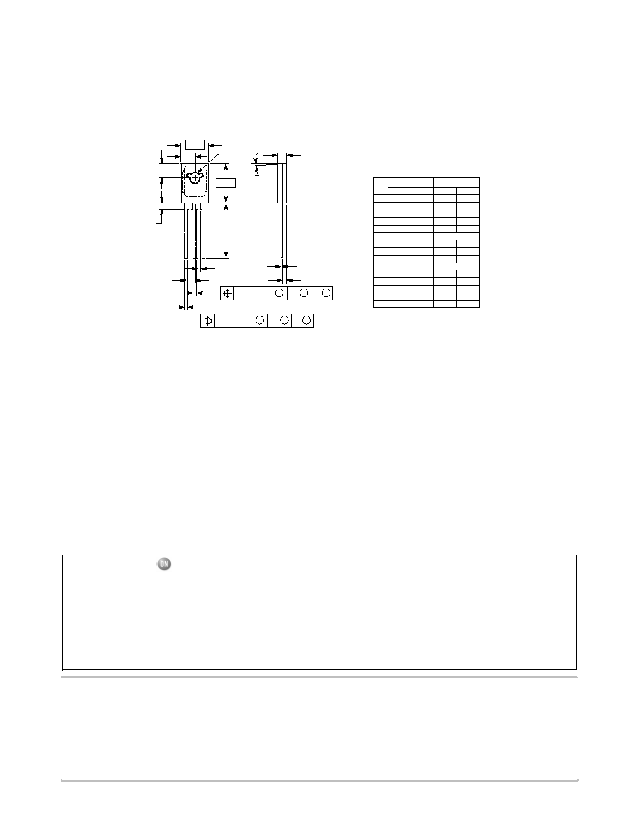
PACKAGE DIMENSIONS
TO≠126
TO≠225AA
CASE 77≠09
ISSUE W
STYLE 1:
PIN 1. EMITTER
2. COLLECTOR
3. BASE
NOTES:
1. DIMENSIONING AND TOLERANCING PER ANSI
Y14.5M, 1982.
2. CONTROLLING DIMENSION: INCH.
≠B≠
≠A≠
M
K
F
C
Q
H
V
G
S
D
J
R
U
1
3
2
2 PL
M
A
M
0.25 (0.010)
B
M
M
A
M
0.25 (0.010)
B
M
DIM
MIN
MAX
MIN
MAX
MILLIMETERS
INCHES
A
0.425
0.435
10.80
11.04
B
0.295
0.305
7.50
7.74
C
0.095
0.105
2.42
2.66
D
0.020
0.026
0.51
0.66
F
0.115
0.130
2.93
3.30
G
0.094 BSC
2.39 BSC
H
0.050
0.095
1.27
2.41
J
0.015
0.025
0.39
0.63
K
0.575
0.655
14.61
16.63
M
5 TYP
5 TYP
Q
0.148
0.158
3.76
4.01
R
0.045
0.065
1.15
1.65
S
0.025
0.035
0.64
0.88
U
0.145
0.155
3.69
3.93
V
0.040
---
1.02
---
_
_
ON Semiconductor and are registered trademarks of Semiconductor Components Industries, LLC (SCILLC). SCILLC reserves the right to make
changes without further notice to any products herein. SCILLC makes no warranty, representation or guarantee regarding the suitability of its products for any
particular purpose, nor does SCILLC assume any liability arising out of the application or use of any product or circuit, and specifically disclaims any and all
liability, including without limitation special, consequential or incidental damages. "Typical" parameters which may be provided in SCILLC data sheets and/or
specifications can and do vary in different applications and actual performance may vary over time. All operating parameters, including "Typicals" must be
validated for each customer application by customer's technical experts. SCILLC does not convey any license under its patent rights nor the rights of others.
SCILLC products are not designed, intended, or authorized for use as components in systems intended for surgical implant into the body, or other applications
intended to support or sustain life, or for any other application in which the failure of the SCILLC product could create a situation where personal injury or death
may occur. Should Buyer purchase or use SCILLC products for any such unintended or unauthorized application, Buyer shall indemnify and hold SCILLC
and its officers, employees, subsidiaries, affiliates, and distributors harmless against all claims, costs, damages, and expenses, and reasonable attorney fees
arising out of, directly or indirectly, any claim of personal injury or death associated with such unintended or unauthorized use, even if such claim alleges that
SCILLC was negligent regarding the design or manufacture of the part. SCILLC is an Equal Opportunity/Affirmative Action Employer.
PUBLICATION ORDERING INFORMATION
JAPAN: ON Semiconductor, Japan Customer Focus Center
4≠32≠1 Nishi≠Gotanda, Shinagawa≠ku, Tokyo, Japan 141≠0031
Phone: 81≠3≠5740≠2700
Email: r14525@onsemi.com
ON Semiconductor Website: http://onsemi.com
For additional information, please contact your local
Sales Representative.
BD676/D
Literature Fulfillment:
Literature Distribution Center for ON Semiconductor
P.O. Box 5163, Denver, Colorado 80217 USA
Phone: 303≠675≠2175 or 800≠344≠3860 Toll Free USA/Canada
Fax: 303≠675≠2176 or 800≠344≠3867 Toll Free USA/Canada
Email: ONlit@hibbertco.com
N. American Technical Support: 800≠282≠9855 Toll Free USA/Canada