 | –≠–ª–µ–∫—Ç—Ä–æ–Ω–Ω—ã–π –∫–æ–º–ø–æ–Ω–µ–Ω—Ç: C106M1G | –°–∫–∞—á–∞—Ç—å:  PDF PDF  ZIP ZIP |

©
Semiconductor Components Industries, LLC, 2005
August, 2005 - Rev. 8
1
Publication Order Number:
C106/D
C106 Series
Preferred Devices
Sensitive Gate Silicon
Controlled Rectifiers
Reverse Blocking Thyristors
Glassivated PNPN devices designed for high volume consumer
applications such as temperature, light, and speed control; process and
remote control, and warning systems where reliability of operation is
important.
Features
∑
Glassivated Surface for Reliability and Uniformity
∑
Power Rated at Economical Prices
∑
Practical Level Triggering and Holding Characteristics
∑
Flat, Rugged, Thermopad Construction for Low Thermal Resistance,
High Heat Dissipation and Durability
∑
Sensitive Gate Triggering
∑
Pb-Free Packages are Available*
*For additional information on our Pb-Free strategy and soldering details, please
download the ON Semiconductor Soldering and Mounting Techniques
Reference Manual, SOLDERRM/D.
TO-225AA
CASE 077
STYLE 2
See detailed ordering and shipping information in the package
dimensions section on page 2 of this data sheet.
ORDERING INFORMATION
SCRs
4 A RMS, 200 - 600 Volts
http://onsemi.com
K
G
A
MARKING DIAGRAM & PIN ASSIGNMENT
Y
= Year
WW
= Work Week
C106xx
= Device Code
xx
= B, D, D1, M, M1
G
= Pb-Free Package
YWW
C106xxG
1. Cathode
2. Anode
3. Gate
C106 Series
http://onsemi.com
2
MAXIMUM RATINGS
(T
J
= 25
∞
C unless otherwise noted)
Characteristic
Symbol
Max
Unit
Peak Repetitive Off-State Voltage (Note 1)
(Sine Wave, 50-60 Hz, R
GK
= 1 k
W
,
T
C
= -40
∞
to 110
∞
C)
C106B
C106D, C106D1*
C106M, C106M1*
V
DRM,
V
RRM
200
400
600
V
On-State RMS Current
(180
∞
Conduction Angles, T
C
= 80
∞
C)
I
T(RMS)
4.0
A
Average On-State Current
(180
∞
Conduction Angles, T
C
= 80
∞
C)
I
T(AV)
2.55
A
Peak Non-Repetitive Surge Current
(1/2 Cycle, Sine Wave, 60 Hz, T
J
= +110
∞
C)
I
TSM
20
A
Circuit Fusing Considerations (t = 8.3 ms)
I
2
t
1.65
A
2
s
Forward Peak Gate Power
(Pulse Width
v
1.0
m
sec, T
C
= 80
∞
C)
P
GM
0.5
W
Forward Average Gate Power
(Pulse Width
v
1.0
m
sec, T
C
= 80
∞
C)
P
G(AV)
0.1
W
Forward Peak Gate Current
(Pulse Width
v
1.0
m
sec, T
C
= 80
∞
C)
I
GM
0.2
A
Operating Junction Temperature Range
T
J
-40 to +110
∞
C
Storage Temperature Range
T
stg
-40 to +150
∞
C
Mounting Torque (Note 2)
-
6.0
in. lb.
Maximum ratings are those values beyond which device damage can occur. Maximum ratings applied to the device are individual stress limit
values (not normal operating conditions) and are not valid simultaneously. If these limits are exceeded, device functional operation is not implied,
damage may occur and reliability may be affected.
1. V
DRM
and V
RRM
for all types can be applied on a continuous basis. Ratings apply for zero or negative gate voltage; however, positive gate
voltage shall not be applied concurrent with negative potential on the anode. Blocking voltages shall not be tested with a constant current
source such that the voltage ratings of the devices are exceeded.
2. Torque rating applies with use of compression washer (B52200F006). Mounting torque in excess of 6 in. lb. does not appreciably lower
case-to-sink thermal resistance. Anode lead and heatsink contact pad are common.
THERMAL CHARACTERISTICS
(T
C
= 25
∞
C unless otherwise noted.)
Characteristic
Symbol
Max
Unit
Thermal Resistance, Junction-to-Case
R
q
JC
3.0
∞
C/W
Thermal Resistance, Junction-to-Ambient
R
q
JA
75
∞
C/W
Maximum Lead Temperature for Soldering Purposes 1/8 in. from Case for 10 Seconds
T
L
260
∞
C
ORDERING INFORMATION
Device
Package
Shipping
C106B
TO-225AA
500 Units / Box
C106BG
TO-225AA
(Pb-Free)
500 Units / Box
C106D
TO-225AA
500 Units / Box
C106DG
TO-225AA
(Pb-Free)
500 Units / Box
C106D1*
TO-225AA
500 Units / Box
C106D1G*
TO-225AA
(Pb-Free)
500 Units / Box
C106M
TO-225AA
500 Units / Box
C106MG
TO-225AA
(Pb-Free)
500 Units / Box
C106M1*
TO-225AA
500 Units / Box
C106M1G*
TO-225AA
(Pb-Free)
500 Units / Box
For information on tape and reel specifications, including part orientation and tape sizes, please refer to our Tape and Reel Packaging
Specifications Brochure, BRD8011/D.
*D1 signifies European equivalent for D suffix and M1 signifies European equivalent for M suffix.

C106 Series
http://onsemi.com
3
ELECTRICAL CHARACTERISTICS
(T
C
= 25
∞
C unless otherwise noted.)
Characteristic
Symbol
Min
Typ
Max
Unit
OFF CHARACTERISTICS
Peak Repetitive Forward or Reverse Blocking Current
(V
AK
= Rated V
DRM
or V
RRM
, R
GK
= 1000 Ohms)
T
J
= 25
∞
C
T
J
= 110
∞
C
I
DRM
, I
RRM
-
-
-
-
10
100
m
A
m
A
ON CHARACTERISTICS
Peak Forward On-State Voltage (Note 3)
(I
TM
= 4 A)
V
TM
-
-
2.2
V
Gate Trigger Current (Continuous dc) (Note 4)
(V
AK
= 6 Vdc, R
L
= 100 Ohms)
T
J
= 25
∞
C
T
J
= -40
∞
C
I
GT
-
-
15
35
200
500
m
A
Peak Reverse Gate Voltage (I
GR
= 10
m
A)
V
GRM
-
-
6.0
V
Gate Trigger Voltage (Continuous dc) (Note 4)
(V
AK
= 6 Vdc, R
L
= 100 Ohms)
T
J
= 25
∞
C
T
J
= -40
∞
C
V
GT
0.4
0.5
0.60
0.75
0.8
1.0
V
Gate Non-Trigger Voltage (Continuous dc) (Note 4)
(V
AK
= 12 V, R
L
= 100 Ohms, T
J
= 110
∞
C)
V
GD
0.2
-
-
V
Latching Current
(V
AK
= 12 V, I
G
= 20 mA)
T
J
= 25
∞
C
T
J
= -40
∞
C
I
L
-
-
0.20
0.35
5.0
7.0
mA
Holding Current (V
D
= 12 Vdc)
(Initiating Current = 20 mA, Gate Open)
T
J
= 25
∞
C
T
J
= -40
∞
C
T
J
= +110
∞
C
I
H
-
-
-
0.19
0.33
0.07
3.0
6.0
2.0
mA
DYNAMIC CHARACTERISTICS
Critical Rate-of-Rise of Off-State Voltage
(V
AK
= Rated V
DRM
, Exponential Waveform, R
GK
= 1000 Ohms,
T
J
= 110
∞
C)
dv/dt
-
8.0
-
V/
m
s
3. Pulse Test: Pulse Width
2.0 ms, Duty Cycle
2%.
4. R
GK
is not included in measurement.
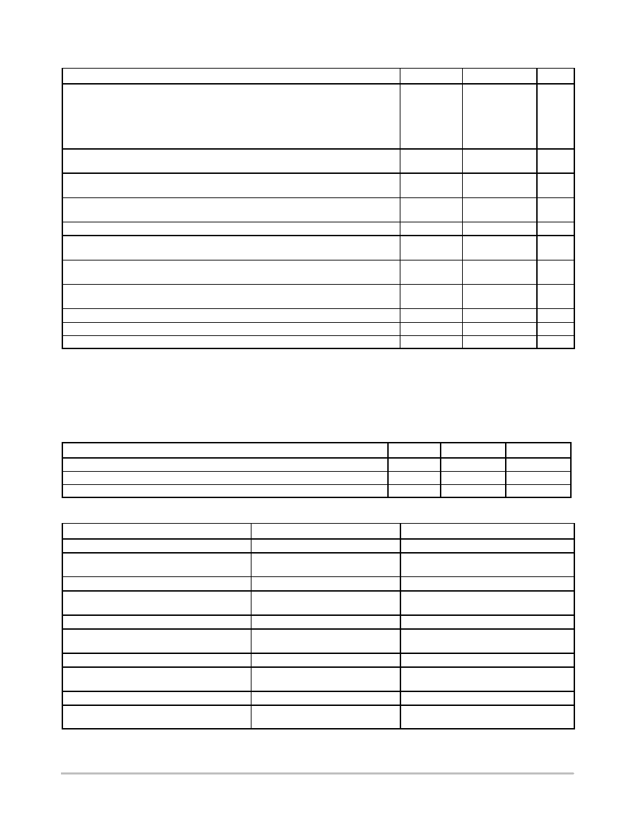
+ Current
+ Voltage
V
TM
I
DRM
at V
DRM
I
H
Symbol
Parameter
V
DRM
Peak Repetitive Off State Forward Voltage
I
DRM
Peak Forward Blocking Current
V
RRM
Peak Repetitive Off State Reverse Voltage
I
RRM
Peak Reverse Blocking Current
V
TM
Peak On State Voltage
I
H
Holding Current
Voltage Current Characteristic of SCR
Anode +
on state
Reverse Blocking Region
(off state)
Reverse Avalanche Region
Anode -
Forward Blocking Region
I
RRM
at V
RRM
(off state)
C106 Series
http://onsemi.com
4
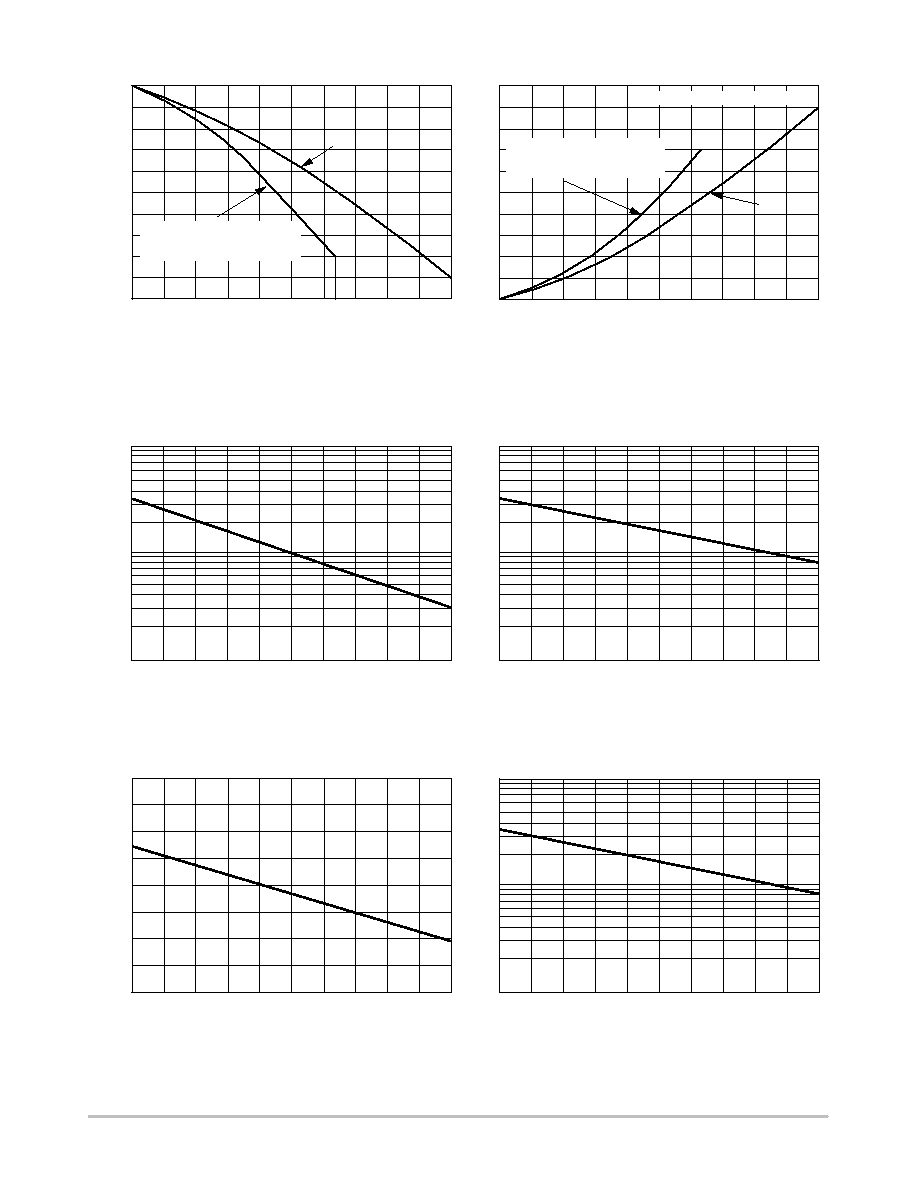
DC
DC
JUNCTION TEMPERATURE 110∞C
100
10
20
30
40
70
110
90
3.6
80
0
.4
.8
1.6
1.2
2.0
2.4
3.2
60
4.0
I
T(AV)
AVERAGE ON-STATE CURRENT (AMPERES)
HALF SINE WAVE
RESISTIVE OR INDUCTIVE LOAD.
50 to 400 Hz
50
6
4
2
0
8
0
10
2.8
3.6
.4
.8
1.6
1.2
2.0
2.4
3.2
4.0
2.6
I
T(AV)
AVERAGE ON-STATE CURRENT (AMPERES)
HALF SINE WAVE
RESISTIVE OR INDUCTIVE LOAD
50 TO 400Hz.
C
∞
T
, CASE
TEMPERATURE ( C)
P
,
A
VERAGE
ON-ST
A
TE
POWER
DISSIP
A
TION
(W
A
TTS)
(A
V)
Figure 1. Average Current Derating
Figure 2. Maximum On-State Power Dissipation
1
100
95
-40 -25 -10
20
5
35
50
80
10
110
T
J
, JUNCTION TEMPERATURE (∞C)
65
GT
m
I
Figure 3. Typical Gate Trigger Current versus
Junction Temperature
Figure 4. Typical Holding Current versus
Junction Temperature
0.9
0.2
0.3
0.4
0.7
1.0
0.8
95
-45 -25 -10
20
5
35
50
80
0.6
110
T
J
, JUNCTION TEMPERATURE (∞C)
0.5
65
GTV
Figure 5. Typical Gate Trigger Voltage versus
Junction Temperature
Figure 6. Typical Latching Current versus
Junction Temperature
,
GA
TE TRIGGER
CURRENT
(
A)
10
1000
95
-40 -25 -10
20
5
35
50
80
100
110
T
J
, JUNCTION TEMPERATURE (∞C)
65
H
m
I
,
HOLDING
CURRENT
(
A)
10
1000
95
-40 -25 -10
20
5
35
50
80
100
110
T
J
, JUNCTION TEMPERATURE (∞C)
65
L
m
I
,
LA
TCHING
CURRENT
(
A)
, GA
TE
TRIGGER
VOL
T
AGE
(V)

C106 Series
http://onsemi.com
5
The dimensional diagrams below compare the critical dimensions of the ON Semiconductor C-106 package with
competitive devices. It has been demonstrated that the smaller dimensions of the ON Semiconductor package make it
compatible in most lead-mount and chassis-mount applications. The user is advised to compare all critical dimensions for
mounting compatibility.
ON Semiconductor C-106 Package
Competitive C-106 Package
.315
____
.285
.105
____
.095
.054
____
.046
.420
____
.400
.400
____
.360
.385
____
.365
.135
____
.115
.520
____
.480
.127
____
.123
DIA
.105
____
.095
.190
____
.170
.026
____
.019
.025
____
.035
.295
____
.305
.148
____
.158
.115
____
.130
_
.015
____
.025
.050
____
.095
.145
____
.155
5 TYP
.425
____
.435
.575
____
.655
.020
____
.026
1 2 3
.045
____
.055
.095
____
.105
.040
.094 BSC
PACKAGE INTERCHANGEABILITY