©
Semiconductor Components Industries, LLC, 2001
August, 2001 ≠ Rev. 11
1
Publication Order Number:
CS1087/D
CS1087
Vacuum Fluorescent
Display Tube Driver
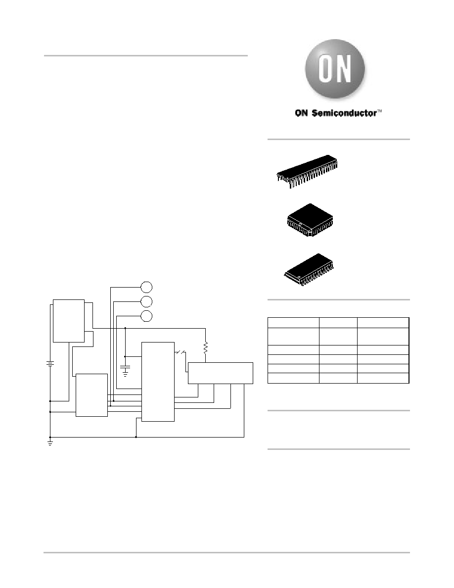
The VFD Driver is a microprocessor interface IC that drives a
multiplexed VF (Vacuum Fluorescent) display tube. It consists of a
32≠bit shift register, a 32≠bit transparent data latch, a metal mask
ROM, six 20 mA anode output drivers, twenty≠three 2 mA anode
output drivers, and three 50 mA grid drivers with output enables.
Features
∑
Power On Reset
∑
Display Dimming Possible
∑
Three, 50 mA Grid Drivers
∑
Anode Options ≠ DIP≠40 and PCLL≠44:
≠
6 @ 20 mA
≠
23 @ 2 mA
∑
Anode Options ≠ SO≠28L:
≠
3 @ 20 mA
≠
15 @ 2 mA
GRID1GRID2 GRID3 GND
FILAMENT
VFD
PORT
PORT
PORT
GND
V
CC
PORT
V
IGN
GND
5 V
12 V
µ
P
Regulator
V
BAT
Data Out
Clock
Chip Select
SPI Functions
Anodes
GREN
STB
CLK
D
IN
D
OUT
CS1087
GRID3
GRID2
GRID1
0.1
µ
F
V
BB
GND
1:29
Figure 1. Application Diagram
Device
http://onsemi.com
Package
Shipping
ORDERING INFORMATION*
DIP≠40
WIDE BODY
9 Units/Rail
PLCC≠44
CS1087XN40
CS1087XFN44
SO≠28L
23 Units/Rail
CS1087XFNR44
500 Tape & Reel
DIP≠40
WIDE BODY
N SUFFIX
CASE 711
PLCC≠44
FN SUFFIX
CASE 777
See general marking information in the device marking
section on page 7 of this data sheet.
DEVICE MARKING INFORMATION
40
1
CS1087XDW28
27 Units/Rail
SO≠28L
CS1087XDWR28
1000 Tape & Reel
PLCC≠44
*For additional package options, consult your local
ON Semiconductor sales office.
SO≠28L
DW SUFFIX
CASE 751F
1
28
CS1087
http://onsemi.com
2
MAXIMUM RATINGS*
Parameter
Value
Unit
Supply Voltage (V
BB
)
≠0.6 to +18
V
Input Voltages (D
IN
, CLK, STB, GREN)
≠0.6 to +6.0
V
Junction Temperature Range
≠40 to +150
∞
C
Storage Temperature Range
≠55 to +150
∞
C
ESD Susceptibility (Human Body Model)
2.0
kV
ESD Susceptibility (Machine Model)
200
V
Package Thermal Resistance, DIP≠40
Junction≠to≠Case, R
JC
Junction≠to≠Ambient, R
JA
20
45
∞
C/W
∞
C/W
Package Thermal Resistance, PLCC≠44
Junction≠to≠Case, R
JC
Junction≠to≠Ambient, R
JA
16
55
∞
C/W
∞
C/W
Package Thermal Resistance, SO≠28L
Junction≠to≠Case, R
JC
Junction≠to≠Ambient, R
JA
15
75
∞
C/W
∞
C/W
Lead Temperature Soldering:
Wave Solder (through hole styles only) Note 1
Reflow (SMD styles only) Note 2
260 Peak
230 Peak
∞
C
1. 10 second maximum.
2. 60 second maximum above 183
∞
C.
*The maximum package power dissipation must be observed.
ELECTRICAL CHARACTERISTICS
(8.0 V
V
BB
16.5 V, Gnd = 0 V, ≠40
∞
C
T
J
105
∞
C; unless otherwise stated. Note 3.)
Parameter
Test Conditions
Min
Typ
Max
Unit
V
BB
Input
V
BB
Input Voltage
≠
8.0
≠
16.5
V
I
BB0
Current
No outputs active, V
BB
= 16.5 V
≠
2.0
5.0
mA
Reset Mode
All outputs forced low.
≠
6.5
7.5
V
D
IN
, CLK, STB Inputs
V
IL1
, Input Low Voltage
≠
≠
≠
1.6
V
V
IH
, Input High Voltage
≠
3.3
≠
≠
V
I
IL
, Input Current
V
IN
= V
IH
≠
7.5
20.0
µ
A
GREN Input
V
IL
, Input Low Voltage
≠
≠
≠
1.6
V
V
IH
, Input High Voltage
≠
3.3
≠
≠
V
I
IH
, Input Pull≠down Current
V
IN
= 3.325 V
≠
30
60
µ
A
GRID1, GRID2, GRID3 Outputs
I
OL
Sink Current
1.0
≠
≠
mA
I
OH
Source Current
50
≠
≠
mA
V
OL
I
OUT
= 1.0 mA
≠
≠
0.5
V
V
OH
I
OUT
= ≠50 mA, V
BB
= 12 V
V
BB
≠ 0.75
≠
V
BB
V
3. Designed to meet these characteristics over the stated voltage and temperature ranges, though may not be 100% parametrically tested
in production.

CS1087
http://onsemi.com
3
ELECTRICAL CHARACTERISTICS (continued)
(8.0 V
V
BB
16.5 V, Gnd = 0 V, ≠40
∞
C
T
J
105
∞
C; unless otherwise stated.
Note 4.)
Parameter
Test Conditions
Min
Typ
Max
Unit
AN24 ≠ AN29 Outputs
I
OL
Sink Current
400
≠
≠
µ
A
I
OH
Source Current
20
≠
≠
mA
V
OL
I
OUT
= 400
µ
A
≠
≠
0.5
V
V
OH
I
OUT
= ≠20 mA, V
BB
= 12 V
V
BB
≠ 0.5
≠
V
BB
V
AN1 ≠ AN23 Outputs
I
OL
Sink Current
100
≠
≠
µ
A
I
OH
Source Current
2.0
≠
≠
mA
V
OL
I
OUT
= 100
µ
A
≠
≠
0.5
V
V
OH
I
OUT
= ≠2.0 mA, V
BB
= 12 V
V
BB
≠ 0.5
≠
V
BB
V
D
OUT
Output
I
OL
Sink Current
1.0
≠
≠
mA
I
OH
Source Current
1.0
≠
≠
mA
V
OL
I
OUT
= 1.0 mA
≠
≠
0.5
V
V
OH
I
OUT
= ≠1.0 mA
3.9
≠
5.1
V
AC Characteristics: Input and Output Timing
F
C
, CLK Frequency
≠
0
≠
1.0
MHz
T
CL
, CLK Low Time
≠
200
≠
≠
ns
T
CH
, CLK High Time
≠
200
≠
≠
ns
T
CR
, CLK Rise Time
≠
≠
≠
100
ns
T
CF
, CLK Fall Time
≠
≠
≠
100
ns
T
CD
, CLK Low to D
OUT
Propagation Delay
≠
≠
≠
200
ns
T
SC
, STB Low to CLK High Time
≠
50
≠
≠
ns
T
ST
, STB High Time
≠
500
≠
≠
ns
T
AN
, STB High to Anode Output
Propagation Delay
≠
≠
≠
5.0
µ
s
T
GL
, Grid Turn On Propagation Delay
V
BB
= 12 V
≠
≠
2.0
µ
s
T
G0
, Grid Turn Off Propagation Delay
V
BB
= 12 V
≠
≠
5.0
µ
s
T
GR
, Grid Rise Time
At rated load. Note 5.
0.50
≠
2.00
µ
s
T
GF
, Grid Fall Time
At rated load. Note 5.
0.35
≠
2.00
µ
s
T
AR
, Anode Rise Time
At rated load. Note 5.
0.40
≠
2.00
µ
s
T
AF
, Anode Fall Time
At rated load. Note 5.
0.40
≠
2.50
µ
s
4. Designed to meet these characteristics over the stated voltage and temperature ranges, though may not be 100% parametrically tested
in production.
5. Grid and anode rise/fall times are measured from 10% and 90% points. Output currents are at the maximum rated currents for the
respective stages.

CS1087
http://onsemi.com
4
PACKAGE LEAD DESCRIPTION
Package Lead Number
Lead Symbol
40L DIP
44L PLCC
SO≠28L
(29 Anode Configuration)
Function
1
14
1
GRID1
50 mA grid output.
2
15
2
GRID2
50 mA grid output.
3
16
3
GRID3
50 mA grid output.
4
17
≠
AN1
2.0 mA anode output.
5
18
4
AN2
2.0 mA anode output.
6
19
5
AN3
2.0 mA anode output.
7
20
6
AN4
2.0 mA anode output.
8
21
≠
AN5
2.0 mA anode output.
9
22
7
AN6
2.0 mA anode output.
10
24
≠
AN7
2.0 mA anode output.
11
25
≠
AN8
2.0 mA anode output.
12
26
8
AN9
2.0 mA anode output.
13
27
≠
AN10
2.0 mA anode output.
14
28
9
AN11
2.0 mA anode output.
15
29
10
AN12
2.0 mA anode output.
16
30
11
AN13
2.0 mA anode output.
17
31
12
AN14
2.0 mA anode output.
18
32
13
AN15
2.0 mA anode output.
19
33
≠
AN16
2.0 mA anode output.
20
35
14
GND
Ground connection.
21
36
15
AN17
2.0 mA anode output.
22
37
≠
AN18
2.0 mA anode output.
23
38
16
AN19
2.0 mA anode output.
24
39
17
AN20
2.0 mA anode output.
25
40
18
AN21
2.0 mA anode output.
26
41
19
AN22
2.0 mA anode output.
27
42
≠
AN23
2.0 mA anode output.
28
43
20
AN24
20 mA anode output.
29
44
21
AN25
20 mA anode output.
30
2
22
AN26
20 mA anode output.
31
3
≠
AN27
20 mA anode output.
32
4
≠
AN28
20 mA anode output.
33
5
≠
AN29
20 mA anode output.
34
6
23
D
OUT
Shift register data output.
35
7
24
D
IN
Shift register data input.
36
8
25
CLK
Shift register clock input.
37
9
26
STB
Transfer contents of shift registers to output stages.
38
10
27
GREN
Grid outputs enable.
39
1, 11, 12, 23, 34
≠
NC
No connection.
40
13
28
V
BB
Supply voltage input.
CS1087
http://onsemi.com
5
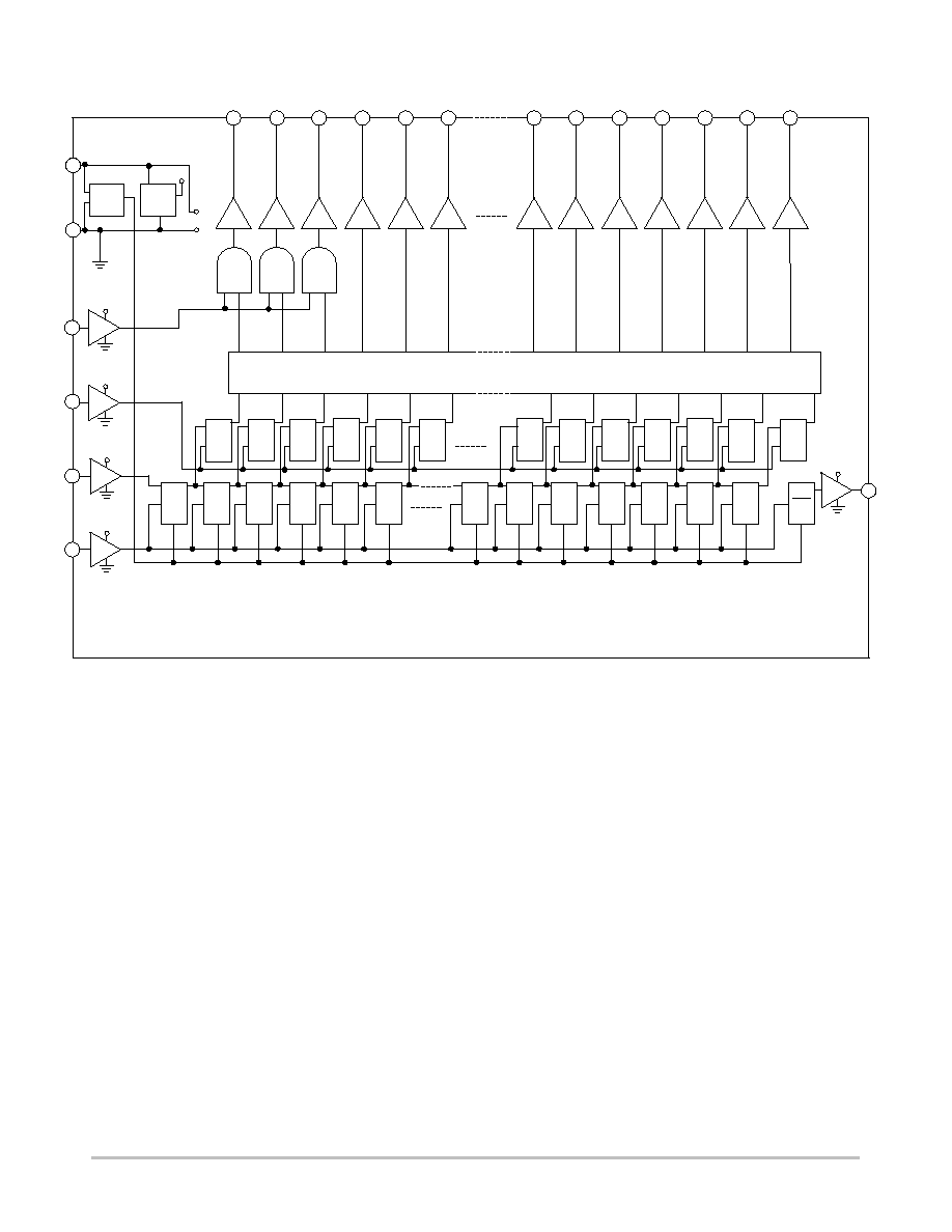
AN1≠AN23: 2.0 mA
V
REG
POR
GRID1
GRID2 GRID3
AN1
AN2
AN3
AN23
AN24
AN25
AN26
AN27
AN28
AN29
V
BB
GND
GREN
STB
D
IN
CLK
D
OUT
METAL MASK ROM
Output Drive Capability
Grid Outputs: 50 mA
AN24≠AN29: 20 mA
D Q
LE
D Q
CLK
R
V
REG
V
REG
V
REG
V
REG
V
REG
V
REG
Figure 2. Block Diagram
D Q
CLK
R
D Q
CLK
R
D Q
CLK
R
D Q
CLK
R
D Q
CLK
R
D Q
CLK
R
D Q
CLK
R
D Q
CLK
R
D Q
CLK
R
D Q
CLK
R
D Q
CLK
R
D Q
CLK
R
D Q
CLK
R
D Q
LE
D Q
LE
D Q
LE
D Q
LE
D Q
LE
D Q
LE
D Q
LE
D Q
LE
D Q
LE
D Q
LE
D Q
LE
D Q
LE
OPERATION DESCRIPTION
Upon the initial application of power, the power on reset
function will cause all of the anode and grid driver outputs
to be off and all shift register outputs to be set low. Data is
fed into the shift register through the D
IN
pin at the rising
edge of the CLK input. Thirty two bits of data are capable of
being stored by the shift register. Once the desired pattern is
stored in the shift register, it can be transferred to the latch
by setting the STB input high. The output of each latch
drives its corresponding output stage. A logic high input to
the shift register/latch will cause the corresponding output
to turn on. A logic low input to the shift register/latch will
cause the corresponding output to turn off. Please note that
if the STB is held high, the outputs of the latch reflect the
outputs of the corresponding shift register bits and will
change if data is shifted in.
The three GRID outputs are gated by the GREN input.
When GREN is low, the GRID outputs are forced low
regardless of the state of the corresponding latch output.
When GREN is high, the GRID outputs correspond to the
state of their respective latch outputs. The anode outputs,
AN1 to AN29 are always enabled.
The D
OUT
pin is the output of the last stage of the shift
register to allow serial cascading of this IC with other
devices. Data from the last stage of the shift register is
supplied to the D
OUT
pin delayed by 1/2 CLK cycle. Data on
the D
OUT
output changes with the falling edges of the CLK
to prevent logic race conditions between the CLK and the
D
IN
of the next IC in the serial chain.
CS1087
http://onsemi.com
6
APPLICATION INFORMATION
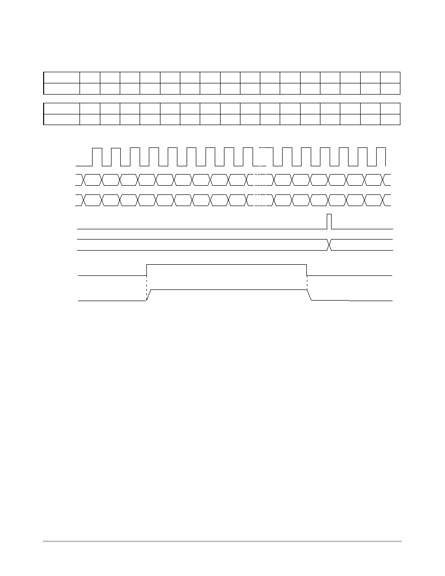
Table 1. Bit Pattern, G = Grid, A = Anode.
Bit #
1
2
3
4
5
6
7
8
9
10
11
12
13
14
15
16
Pin Name
G1
G2
G3
A1
A2
A3
A4
A5
A6
A7
A8
A9
A10
A11
A12
A13
Bit #
17
18
19
20
21
22
23
24
25
26
27
28
29
30
31
32
Pin Name
A14
A15
A16
A17
A18
A19
A20
A21
A22
A23
A24
A25
A26
A27
A28
A29
2
3
4
5
6
7
8
9
30
31
32
1
2
3
1
CLK
IN
BIT 1
BIT 2
BIT 3
BIT 4
BIT 5
BIT 6
BIT 7
BIT 8
BIT 9
BIT 30 BIT 31 BIT 32
BIT 1
BIT 2
BIT 3
D
IN
BIT 1
BIT 2
BIT 3
BIT 4
BIT 5
BIT 6
BIT 7
BIT 8
BIT 9
BIT 30
BIT 31
BIT 32
BIT 1
BIT 2
BIT 3
D
OUT
PREV
PREV
PREV
PREV
PREV
PREV
PREV
PREV
PREV
PREV
PREV
PREV
PREV
PREV
PREV
STB
ANODES
GREN
GRIDS *
* Selected grid goes high only if input bit pattern from shift register to grid is high.
Figure 3. Typical Operation
Unused grid and anode drivers should have their
respective bits set to logic low in the data stream.
Multiple grid or anode drivers may be connected together,
but must be programmed to the same logic state for proper
device operation. Maximum package power must be
observed and care must be taken to maintian junction
temperature below +150
∞
C.
Care must be taken when interfacing this part to a
microprocessor. The D
OUT
output V
OH
is specified at 3.9 V
to 5.1 V at an I
OUT
of ≠1.0 mA. Lower current loads will
result in a higher output voltage. V
OH
= 5.2 V (typ) with no
load. V
OH
= 5.7 V (max) with no load. Protection or
workarounds for the device may be needed at the application
level. No protection is needed when interfacing with other
parts in this family (CS1087, CS1088, or CS1089).
CS1087
http://onsemi.com
7
PIN CONNECTIONS
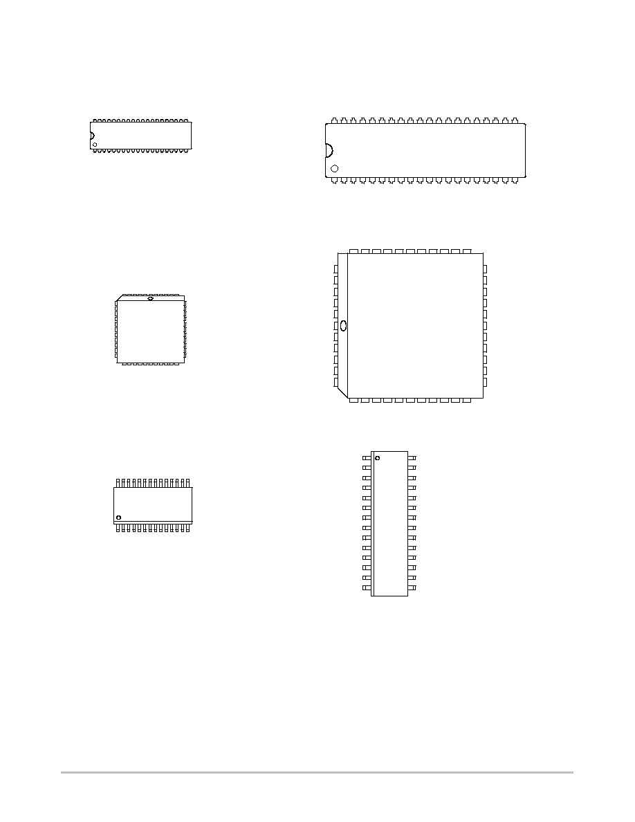
MARKING DIAGRAMS
DIP≠40
WIDE BODY
N SUFFIX
CASE 711
40
1
CS1087
AWLYYWW
40
1
AN17
GND
AN18
AN16
AN19
AN15
AN20
AN14
AN21
AN13
AN22
AN12
AN23
AN1
1
AN24
AN10
AN25
AN9
AN26
AN8
AN27
AN7
AN28
AN6
AN29
AN5
D
OUT
AN4
D
IN
AN3
CLK
AN2
STB
AN1
GREN
GRID3
NC
GRID2
V
BB
GRID1
PLCC≠44
FN SUFFIX
CASE 777
CS1087
AWLYYWW
1
AN11
AN21
1
2
3
4
44
43
42
41
40
5
6
7 8
9 10 11 12 13 14 15 16 17
18
19
20
21
22
23
24
25
26
27
28
29
30
31
32
33
34
35
36
37
38
39
AN10
AN9
AN8
AN7
NC
AN6
AN5
AN4
AN3
AN2
AN22
AN23
AN24
AN25
NC
AN26
AN27
AN28
AN29
D
OUT
AN20
D
IN
AN19
AN18
AN17
GND
NC
AN16
AN15
AN14
AN13
AN12
CLK
STB
GREN
NC
NC
V
BB
GRID1
GRID2
GRID3
AN1
A
= Assembly Location
WL, L
= Wafer Lot
YY, Y
= Year
WW, W = Work Week
1
CS1087
AWLYYWW
28
1
28
AN25
AN9
AN26
AN6
D
OUT
AN4
D
IN
AN3
CLK
AN2
STB
GRID3
GREN
GRID2
V
BB
GRID1
AN24
AN11
AN22
AN12
AN20
AN14
AN21
AN13
AN19
AN15
AN17
GND
SO≠28L
DW SUFFIX
CASE 751F

CS1087
http://onsemi.com
8
PACKAGE DIMENSIONS
NOTES:
1. POSITIONAL TOLERANCE OF LEADS (D), SHALL
BE WITHIN 0.25 (0.010) AT MAXIMUM MATERIAL
CONDITION, IN RELATION TO SEATING PLANE
AND EACH OTHER.
2. DIMENSION L TO CENTER OF LEADS WHEN
FORMED PARALLEL.
3. DIMENSION B DOES NOT INCLUDE MOLD FLASH.
1
20
40
21
B
A
C
SEATING
PLANE
D
F
G
H
K
N
M
J
L
DIM
MIN
MAX
MIN
MAX
INCHES
MILLIMETERS
A
51.69
52.45
2.035
2.065
B
13.72
14.22
0.540
0.560
C
3.94
5.08
0.155
0.200
D
0.36
0.56
0.014
0.022
F
1.02
1.52
0.040
0.060
G
2.54 BSC
0.100 BSC
H
1.65
2.16
0.065
0.085
J
0.20
0.38
0.008
0.015
K
2.92
3.43
0.115
0.135
L
15.24 BSC
0.600 BSC
M
0
15
0
15
N
0.51
1.02
0.020
0.040
_
_
_
_
DIP≠40
WIDE BODY
N SUFFIX
CASE 711≠03
ISSUE C
CS1087
http://onsemi.com
9
PACKAGE DIMENSIONS
NOTES:
1. DATUMS -L-, -M-, AND -N- ARE DETERMINED
WHERE TOP OF LEAD SHOULDER EXITS
PLASTIC BODY AT MOLD PARTING LINE.
2. DIMENSION G1, TRUE POSITION TO BE
MEASURED AT DATUM -T-, SEATING PLANE.
3. DIMENSIONS R AND U DO NOT INCLUDE MOLD
FLASH. ALLOWABLE MOLD FLASH IS 0.010
(0.25) PER SIDE.
4. DIMENSIONING AND TOLERANCING PER ANSI
Y14.5M, 1982.
5. CONTROLLING DIMENSION: INCH.
6. THE PACKAGE TOP MAY BE SMALLER THAN
THE PACKAGE BOTTOM BY UP TO 0.012
(0.300). DIMENSIONS R AND U ARE
DETERMINED AT THE OUTERMOST
EXTREMES OF THE PLASTIC BODY
EXCLUSIVE OF MOLD FLASH, TIE BAR BURRS,
GATE BURRS AND INTERLEAD FLASH, BUT
INCLUDING ANY MISMATCH BETWEEN THE
TOP AND BOTTOM OF THE PLASTIC BODY.
7. DIMENSION H DOES NOT INCLUDE DAMBAR
PROTRUSION OR INTRUSION. THE DAMBAR
PROTRUSION(S) SHALL NOT CAUSE THE H
DIMENSION TO BE GREATER THAN 0.037
(0.940). THE DAMBAR INTRUSION(S) SHALL
NOT CAUSE THE H DIMENSION TO BE
SMALLER THAN 0.025 (0.635).
≠N≠
≠L≠
≠M≠
D
Y
D
K
V
W
1
44
BRK
B
Z
U
X
VIEW D≠D
S
L-M
M
0.007(0.180)
N
S
T
S
L-M
M
0.007(0.180)
N
S
T
G1
S
L-M
S
0.010 (0.25)
N
S
T
K1
F
H
S
L-M
M
0.007(0.180)
N
S
T
Z
G
G1
R
A
E
J
VIEW S
C
S
L-M
M
0.007(0.180)
N
S
T
S
L-M
M
0.007(0.180)
N
S
T
0.004 (0.10)
≠T≠
SEATING
PLANE
VIEW S
DIM
MIN
MAX
MIN
MAX
MILLIMETERS
INCHES
A
0.685
0.695
17.40
17.65
B
0.685
0.695
17.40
17.65
C
0.165
0.180
4.20
4.57
E
0.090
0.110
2.29
2.79
F
0.013
0.019
0.33
0.48
G
0.050 BSC
1.27 BSC
H
0.026
0.032
0.66
0.81
J
0.020
---
0.51
---
K
0.025
---
0.64
---
R
0.650
0.656
16.51
16.66
U
0.650
0.656
16.51
16.66
V
0.042
0.048
1.07
1.21
W
0.042
0.048
1.07
1.21
X
0.042
0.056
1.07
1.42
Y
---
0.020
---
0.50
Z
2
10
2
10
G1
0.610
0.630
15.50
16.00
K1
0.040
---
1.02
---
S
L-M
S
0.010 (0.25)
N
S
T
S
L-M
M
0.007(0.180)
N
S
T
_
_
_
_
SCALE 1:1
PLCC≠44
FN SUFFIX
CASE 777≠02
ISSUE C
CS1087
http://onsemi.com
10
PACKAGE DIMENSIONS
SO≠28L
DW SUFFIX
CASE 751F≠05
ISSUE G
A1
1
15
14
28
B
S
X
M
0.025
Y
S
T
M
0.25
Y
M
SEATING
PLANE
A
DIM
MIN
MAX
MILLIMETERS
A
2.35
2.65
A1
0.13
0.29
B
0.35
0.49
C
0.23
0.32
D
17.80
18.05
E
7.40
7.60
G
1.27 BSC
H
10.05
10.55
L
0.41
0.90
M
0
8
_
_
L
C
PIN 1 IDENT
D
E
H
0.10
≠X≠
≠Y≠
G
≠T≠
M
NOTES:
1. DIMENSIONING AND TOLERANCING PER ANSI
Y14.5M, 1982.
2. CONTROLLING DIMENSION: MILLIMETER.
3. DIMENSIONS D AND E DO NOT INCLUDE MOLD
PROTRUSION
4. MAXIMUM MOLD PROTRUSION 0.15 PER SIDE.
5. DIMENSION B DOES NOT INCLUDE DAMBAR
PROTRUSION. ALLOWABLE DAMBER
PR5OTRUSION SHALL NOT BE 0.13 TOTATL IN
EXCESS OF B DIMENSION AT MAXIMUM
MATERIAL CONDITION.

CS1087
http://onsemi.com
11
Notes
CS1087
http://onsemi.com
12
ON Semiconductor and are trademarks of Semiconductor Components Industries, LLC (SCILLC). SCILLC reserves the right to make changes
without further notice to any products herein. SCILLC makes no warranty, representation or guarantee regarding the suitability of its products for any particular
purpose, nor does SCILLC assume any liability arising out of the application or use of any product or circuit, and specifically disclaims any and all liability,
including without limitation special, consequential or incidental damages. "Typical" parameters which may be provided in SCILLC data sheets and/or
specifications can and do vary in different applications and actual performance may vary over time. All operating parameters, including "Typicals" must be
validated for each customer application by customer's technical experts. SCILLC does not convey any license under its patent rights nor the rights of others.
SCILLC products are not designed, intended, or authorized for use as components in systems intended for surgical implant into the body, or other applications
intended to support or sustain life, or for any other application in which the failure of the SCILLC product could create a situation where personal injury or
death may occur. Should Buyer purchase or use SCILLC products for any such unintended or unauthorized application, Buyer shall indemnify and hold
SCILLC and its officers, employees, subsidiaries, affiliates, and distributors harmless against all claims, costs, damages, and expenses, and reasonable
attorney fees arising out of, directly or indirectly, any claim of personal injury or death associated with such unintended or unauthorized use, even if such claim
alleges that SCILLC was negligent regarding the design or manufacture of the part. SCILLC is an Equal Opportunity/Affirmative Action Employer.
PUBLICATION ORDERING INFORMATION
JAPAN: ON Semiconductor, Japan Customer Focus Center
4≠32≠1 Nishi≠Gotanda, Shinagawa≠ku, Tokyo, Japan 141≠0031
Phone: 81≠3≠5740≠2700
Email: r14525@onsemi.com
ON Semiconductor Website: http://onsemi.com
For additional information, please contact your local
Sales Representative.
CS1087/D
Literature Fulfillment:
Literature Distribution Center for ON Semiconductor
P.O. Box 5163, Denver, Colorado 80217 USA
Phone: 303≠675≠2175 or 800≠344≠3860 Toll Free USA/Canada
Fax: 303≠675≠2176 or 800≠344≠3867 Toll Free USA/Canada
Email: ONlit@hibbertco.com
N. American Technical Support: 800≠282≠9855 Toll Free USA/Canada