й
Semiconductor Components Industries, LLC, 2001
June, 2001 н Rev. 3
1
Publication Order Number:
CS2842A/D
CS2842A, CS3842A,
CS2843A, CS3843A
Off-Line Current Mode
PWM Control Circuit with
Undervoltage Lockout
The CS284XA, CS384XA provides all the necessary features to
implement offнline fixed frequency currentнmode control with a
minimum number of external components.
T h e C S 3 8 4 X A f a m i l y i n c o r p o r a t e s a n e w p r e c i s i o n
temperatureнcontrolled oscillator with an internally trimmed
discharge current to minimize variations in frequency. A precision
dutyнcycle clamp eliminates the need for an external oscillator when a
50% dutyнcycle is used. Dutyнcycles greater than 50% are also
possible. On board logic ensures that V
REF
is stabilized before the
output stage is enabled. Ion implant resistors provide tighter control of
undervoltage lockout.
Other features include low startup current, pulseнbyнpulse current
limiting, and a highнcurrent totem pole output for driving capacitive
loads, such as the gate of power MOSFET. The output is LOW in the
off state, consistent with Nнchannel devices.
The CS384XA series of currentнmode control ICs are available in
8 and14 lead packages for surface mount (SO) applications as well as
8 lead PDIP packages.
Features
╖
Optimized for Offнline Control
╖
Internally Trimmed Temperature Compensated Oscillator
╖
Maximum DutyнCycle Clamp
╖
V
REF
Stabilized Before Output Stage is Enabled
╖
Low Startup Current
╖
PulseнByнPulse Current Limiting
╖
Improved Undervoltage Lockout
╖
Double Pulse Suppression
╖
1.0% Trimmed Bandgap Reference
╖
High Current Totem Pole Output
http://onsemi.com
x
= 2 or 3
y
= 2 or 3
A
= Assembly Location
WL, L
= Wafer Lot
YY, Y
= Year
WW, W = Work Week
DIPн8
N SUFFIX
CASE 626
1
8
SOн8
D SUFFIX
CASE 751
1
8
SOн14
D SUFFIX
CASE 751A
1
14
1
8
x84yA
AWL
YYWW
MARKING
DIAGRAM
1
x84yA
ALYWX
8
1
CSx84yA
AWLYWW
14
See detailed ordering and shipping information in the package
dimensions section on page 8 of this data sheet.
ORDERING INFORMATION

CS2842A, CS3842A, CS2843A, CS3843A
http://onsemi.com
2
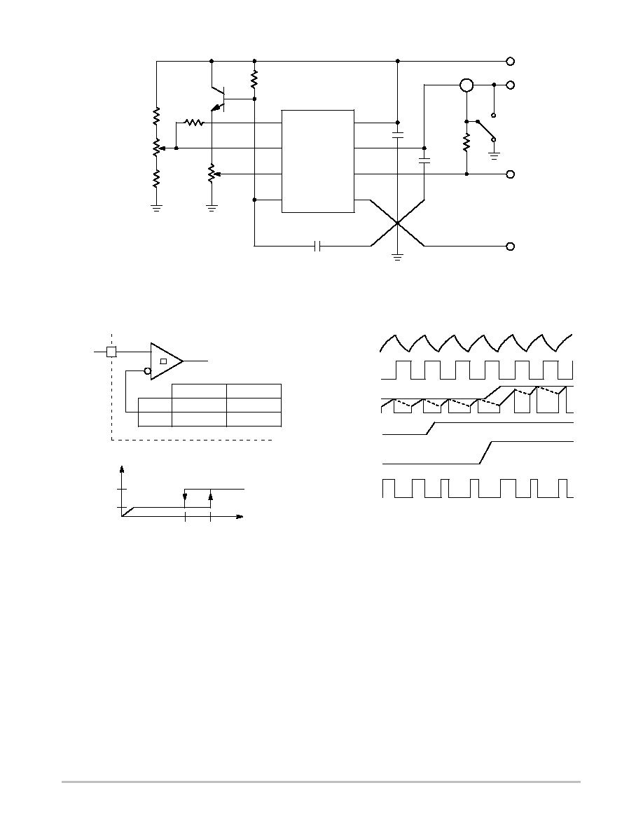
PIN CONNECTIONS
GND
OSC
V
OUT
Sense
V
CC
V
FB
V
REF
COMP
1
GND
OSC
Pwr GND
NC
V
OUT
Sense
V
CC
Pwr
NC
1
14
V
CC
V
FB
NC
NC
V
REF
COMP
8
DIPн8 & SOн8
SOн14
Figure 1. Block Diagram
Set/
Reset
5.0 V
Reference
Undervoltage
Lockнout Circuit
16 V/10 V
(8.4 V/7.6 V)
34 V
V
CC
GND
Output
Enable
Internal
Bias
Oscillator
OSC
2.50 V
V
CC
Pwr
V
REF
V
OUT
+
н
V
FB
COMP
Error
Amplifier
S
R
V
C
2R
R
1.0 V
Sense
Current
Sensing
Comparator
PWM
Latch
Pwr GND
( ) Indicates CS2843A/3843A
NOR
CS2842A, CS3842A, CS2843A, CS3843A
http://onsemi.com
3
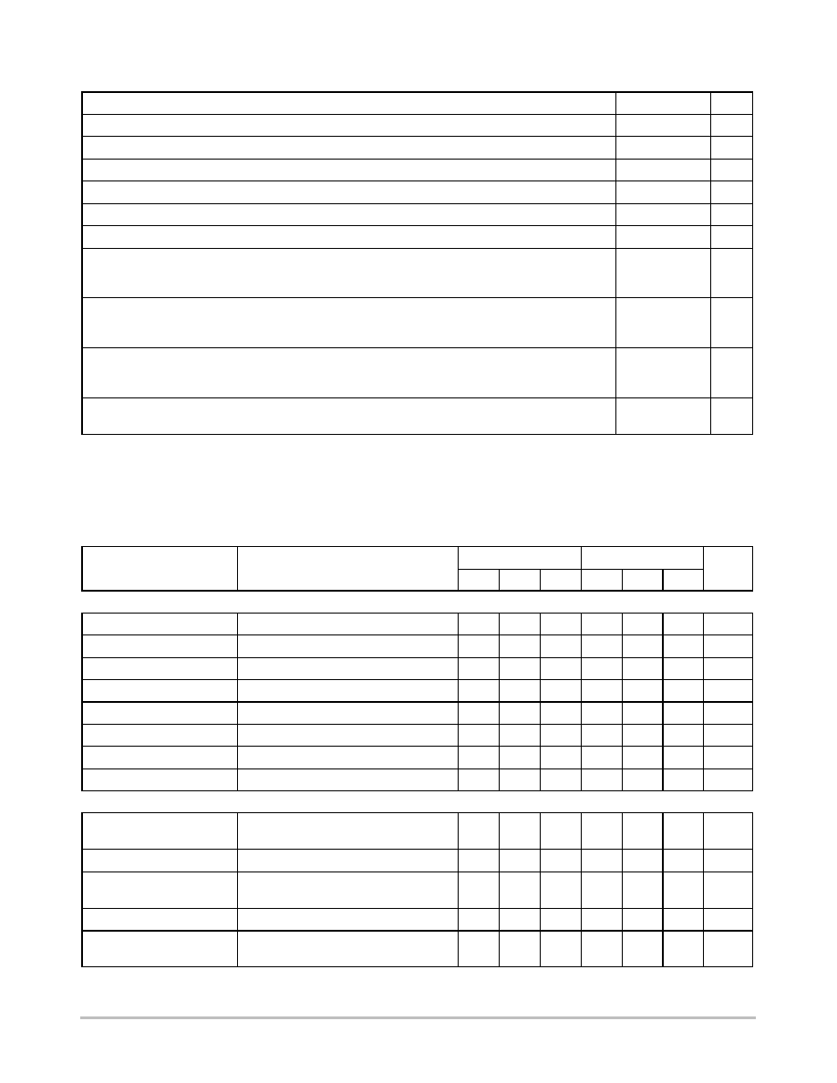
MAXIMUM RATINGS*
Rating
Value
Unit
Supply Voltage (I
CC
< 30 mA)
Self Limiting
н
Supply Voltage (Low Impedance Source)
30
V
Output Current
▒
1.0
A
Output Energy (Capacitive Load)
5.0
╡
J
Analog Inputs (V
FB
, Sense)
н0.3 to + 5.5
V
Error Amp Output Sink Current
10
mA
Package Thermal Resistance, PDIPн8
JunctionнtoнCase, R
JC
JunctionнtoнAmbient, R
JA
52
100
░
CW
░
CW
Package Thermal Resistance, SOн8
JunctionнtoнCase, R
JC
JunctionнtoнAmbient, R
JA
45
165
░
CW
░
CW
Package Thermal Resistance, SOн14
JunctionнtoнCase, R
JC
JunctionнtoнAmbient, R
JA
30
125
░
CW
░
CW
Lead Temperature Soldering:
Wave Solder (through hole styles only) (Note 1)
Reflow (SMD styles only) (Note 2)
260 peak
230 peak
░
C
░
C
1. 10 second maximum.
2. 60 second maximum above 183
░
C.
*The maximum package power dissipation must be observed.
ELECTRICAL CHARACTERISTICS
(н25
░
T
A
85
░
for CS2842A/CS2843A, 0
░
T
A
70
░
for CS3842A/CS3843A.
V
CC
= 15 V*; R
T
= 680
, C
T
= 0.022
╡
F for triangular mode, R
T
= 10 k
, C
T
= 3.3 nF for sawtooth mode (see Figure 7);
unless otherwise stated.)
CS2842A/CS2843A
CS3842A/CS3843A
Characteristic
Test Conditions
Min
Typ
Max
Min
Typ
Max
Unit
Reference Section
Output Voltage
T
J
= 25
░
C, I
OUT
= 1.0 mA
4.95
5.00
5.05
4.90
5.00
5.10
V
Line Regulation
12
V
IN
25 V
н
6.0
20
н
6.0
20
mV
Load Regulation
1.0
I
OUT
20 mA
н
6.0
25
н
6.0
25
mV
Temperature Stability
Note 3.
н
0.2
0.4
н
0.2
0.4
mV/
░
C
Total Output Variation
Line, Load, Temperature (Note 3.)
4.90
н
5.10
4.82
н
5.18
V
Output Noise Voltage
10 Hz
f
10 kHz, T
J
= 25
░
C (Note 3.)
н
50
н
н
50
н
╡
V
Long Term Stability
T
A
= 125
░
C, 1.0 kHrs. (Note 3.)
н
5.0
25
н
5.0
25
mV
Output Short Circuit
T
A
= 25
░
C
н30
н100
н180
н30
н100
н180
mA
Oscillator Section
Initial Accuracy
Sawtooth Mode (see Figure 7), T
J
= 25
░
C
Triangular Mode (see Figure 7), T
J
= 25
░
C
47
47
52
52
57
57
47
44
52
52
57
60
kHz
kHz
Voltage Stability
12
V
CC
25 V
н
0.2
1.0
н
0.2
1.0
%
Temperature Stability
Sawtooth Mode T
MIN
T
A
T
MAX
(Note 3.)
Triangular Mode T
MIN
T
A
T
MAX
(Note 3.)
н
н
5.0
8.0
н
н
н
н
5.0
8.0
н
н
%
%
Amplitude
OSC peak to peak
н
1.7
н
н
1.7
н
V
Discharge Current
T
J
= 25
░
C
T
MIN
T
A
T
MAX
7.5
7.2
8.3
н
9.3
9.5
7.5
7.2
8.3
н
9.3
9.5
mA
mA
3. These parameters, although guaranteed, are not 100% tested in production.
*Adjust V
CC
above the start threshold before setting at 15 V.

CS2842A, CS3842A, CS2843A, CS3843A
http://onsemi.com
4
ELECTRICAL CHARACTERISTICS (continued)
(н25
░
T
A
85
░
for CS2842A/CS2843A, 0
░
T
A
70
░
for CS3842A/CS3843A.
V
CC
= 15 V*; R
T
= 680
, C
T
= 0.022
╡
F for triangular mode, R
T
= 10 k
, C
T
= 3.3 nF for sawtooth mode (see Figure 7);
unless otherwise stated.)
CS2842A/CS2843A
CS3842A/CS3843A
Characteristic
Test Conditions
Min
Typ
Max
Min
Typ
Max
Unit
Error Amp Section
Input Voltage
V
COMP
= 2.5 V
2.45
2.50
2.55
2.42
2.50
2.58
V
Input Bias Current
V
FB
= 0
н
н0.3
н1.0
н
н0.3
н2.0
╡
A
A
VOL
2.0
V
OUT
4.0 V
65
90
н
65
90
н
dB
Unity Gain Bandwidth
Note 4.
0.7
1.0
н
0.7
1.0
н
MHz
PSRR
12
V
CC
25 V
60
70
н
60
70
н
dB
Output Sink Current
V
FB
= 2.7 V, V
COMP
= 1.1 V
2.0
6.0
н
2.0
6.0
н
mA
Output Source Current
V
FB
= 2.3 V, V
COMP
= 5.0 V
н0.5
н0.8
н
н0.5
н0.8
н
mA
V
OUT
High
V
FB
= 2.3 V, 15 k
to ground
5.0
6.0
н
5.0
6.0
н
V
V
OUT
Low
V
FB
= 2.7 V, 15 k
to V
REF
н
0.7
1.1
н
0.7
1.1
V
Current Sense Section
Gain
Notes 5 & 6.
2.85
3.00
3.15
2.85
3.00
3.15
V/V
Maximum Input Signal
V
COMP
= 5.0 V (Note 5.)
0.9
1.0
1.1
0.9
1.0
1.1
V
PSRR
12
V
CC
25 V (Note 5.)
н
70
н
н
70
н
dB
Input Bias Current
V
SENSE
= 0
н
н2.0
н10
н
н2.0
н10
╡
A
Delay to Output
T
J
= 25
░
C (Note 4.)
н
150
300
н
150
300
ns
Output Section
Output Low Level
I
SINK
= 20 mA
I
SINK
= 200 mA
н
н
0.1
1.5
0.4
2.2
н
н
0.1
1.5
0.4
2.2
V
V
Output High Level
I
SOURCE
= 20 mA
I
SOURCE
= 200 mA
13
12
13.5
13.5
н
н
13
12
13.5
13.5
н
н
V
V
Rise Time
T
J
= 25
░
C, C
L
= 1.0 nF (Note 4.)
н
50
150
н
50
150
ns
Fall Time
T
J
= 25
░
C, C
L
= 1.0 nF (Note 4.)
н
50
150
н
50
150
ns
Output Leakage
UVLO Active, V
OUT
= 0
н
н0.01
н10.00
н
н0.01
н10.00
╡
A
Total Standby Current
Startup Current
н
н
0.5
1.0
н
0.5
1.0
mA
Operating Supply Current
V
FB
= V
SENSE
= 0 V,
R
T
= 10 k
, C
T
= 3.3 nF
11
17
н
11
17
н
mA
V
CC
Zener Voltage
I
CC
= 25 mA
н
34
н
н
34
н
V
4. These parameters, although guaranteed, are not 100% tested in production.
5. Parameters measured at trip point of latch with V
FB
= 0.
6. Gain defined as: A =
V
COMP
/
V
SENSE
; 0
V
SENSE
0.8 V.
*Adjust V
CC
above the start threshold before setting at 15 V.

CS2842A, CS3842A, CS2843A, CS3843A
http://onsemi.com
5
ELECTRICAL CHARACTERISTICS (continued)
(н25
░
T
A
85
░
for CS2842A/CS2843A, 0
░
T
A
70
░
for CS3842A/CS3843A.
V
CC
= 15 V*; R
T
= 680
, C
T
= 0.022
╡
F for triangular mode, R
T
= 10 k
, C
T
= 3.3 nF for sawtooth mode (see Figure 7);
unless otherwise stated.)
CS2842A
CS3842A
CS2843A/CS3843A
Characteristic
Test Conditions
Min
Typ
Max
Min
Typ
Max
Min
Typ
Max
Unit
Undervoltage Lockout Section
Start Threshold
н
15
16
17
14.5
16
17.5
7.8
8.4
9.0
V
Min. Operating Voltage
After Turn On
9.0
10
11
8.5
10
11.5
7.0
7.6
8.2
V
*Adjust V
CC
above the start threshold before setting at 15 V.
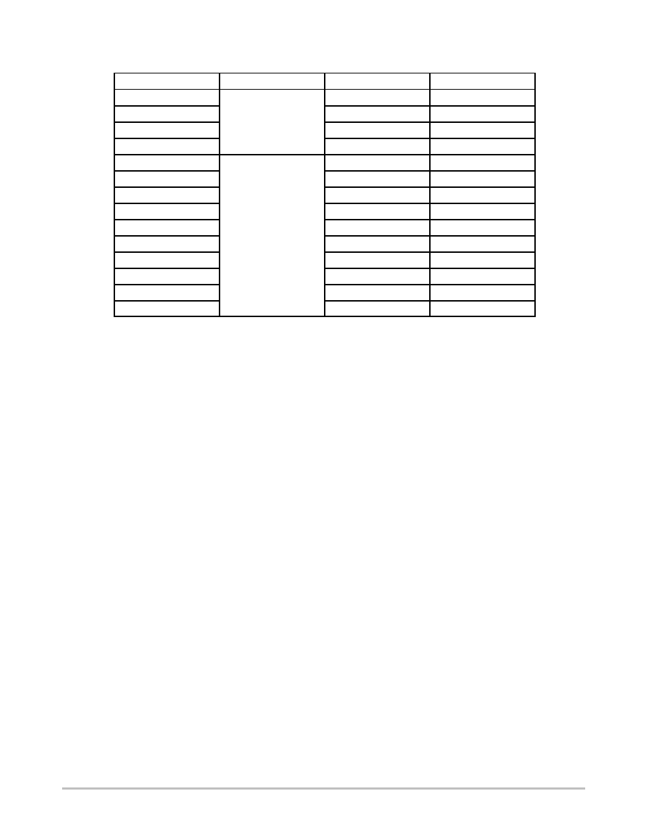
PACKAGE PIN DESCRIPTION
Package Pin Number
DIPн8
SOн8
SOн14
Symbol
Description
┴┴┴┴┴
┴┴┴┴┴
1
┴┴┴┴
┴┴┴┴
1
┴┴┴┴
┴┴┴┴
1
┴┴┴┴┴
┴┴┴┴┴
COMP
┴┴┴┴┴┴┴┴┴┴┴┴┴┴┴┴┴┴┴
┴┴┴┴┴┴┴┴┴┴┴┴┴┴┴┴┴┴┴
Error amp output, used to compensate error amplifier.
┴┴┴┴┴
┴┴┴┴┴
2
┴┴┴┴
┴┴┴┴
2
┴┴┴┴
┴┴┴┴
3
┴┴┴┴┴
┴┴┴┴┴
V
FB
┴┴┴┴┴┴┴┴┴┴┴┴┴┴┴┴┴┴┴
┴┴┴┴┴┴┴┴┴┴┴┴┴┴┴┴┴┴┴
Error amp inverting input.
┴┴┴┴┴
┴┴┴┴┴
3
┴┴┴┴
┴┴┴┴
3
┴┴┴┴
┴┴┴┴
5
┴┴┴┴┴
┴┴┴┴┴
Sense
┴┴┴┴┴┴┴┴┴┴┴┴┴┴┴┴┴┴┴
┴┴┴┴┴┴┴┴┴┴┴┴┴┴┴┴┴┴┴
Noninverting input to Current Sense Comparator.
┴┴┴┴┴
┴┴┴┴┴
4
┴┴┴┴
┴┴┴┴
4
┴┴┴┴
┴┴┴┴
7
┴┴┴┴┴
┴┴┴┴┴
OSC
┴┴┴┴┴┴┴┴┴┴┴┴┴┴┴┴┴┴┴
┴┴┴┴┴┴┴┴┴┴┴┴┴┴┴┴┴┴┴
Oscillator timing network with capacitor to ground, resistor to V
REF.
┴┴┴┴┴
┴┴┴┴┴
5
┴┴┴┴
┴┴┴┴
5
┴┴┴┴
┴┴┴┴
8
┴┴┴┴┴
┴┴┴┴┴
GND
┴┴┴┴┴┴┴┴┴┴┴┴┴┴┴┴┴┴┴
┴┴┴┴┴┴┴┴┴┴┴┴┴┴┴┴┴┴┴
Ground.
┴┴┴┴┴
┴┴┴┴┴
н
┴┴┴┴
┴┴┴┴
н
┴┴┴┴
┴┴┴┴
9
┴┴┴┴┴
┴┴┴┴┴
Pwr GND
┴┴┴┴┴┴┴┴┴┴┴┴┴┴┴┴┴┴┴
┴┴┴┴┴┴┴┴┴┴┴┴┴┴┴┴┴┴┴
Output driver ground.
┴┴┴┴┴
┴┴┴┴┴
6
┴┴┴┴
┴┴┴┴
6
┴┴┴┴
┴┴┴┴
10
┴┴┴┴┴
┴┴┴┴┴
V
OUT
┴┴┴┴┴┴┴┴┴┴┴┴┴┴┴┴┴┴┴
┴┴┴┴┴┴┴┴┴┴┴┴┴┴┴┴┴┴┴
Output drive pin.
┴┴┴┴┴
┴┴┴┴┴
н
┴┴┴┴
┴┴┴┴
н
┴┴┴┴
┴┴┴┴
11
┴┴┴┴┴
┴┴┴┴┴
V
CC
Pwr
┴┴┴┴┴┴┴┴┴┴┴┴┴┴┴┴┴┴┴
┴┴┴┴┴┴┴┴┴┴┴┴┴┴┴┴┴┴┴
Output driver positive supply.
┴┴┴┴┴
┴┴┴┴┴
7
┴┴┴┴
┴┴┴┴
7
┴┴┴┴
┴┴┴┴
12
┴┴┴┴┴
┴┴┴┴┴
V
CC
┴┴┴┴┴┴┴┴┴┴┴┴┴┴┴┴┴┴┴
┴┴┴┴┴┴┴┴┴┴┴┴┴┴┴┴┴┴┴
Positive power supply.
┴┴┴┴┴
┴┴┴┴┴
8
┴┴┴┴
┴┴┴┴
8
┴┴┴┴
┴┴┴┴
14
┴┴┴┴┴
┴┴┴┴┴
V
REF
┴┴┴┴┴┴┴┴┴┴┴┴┴┴┴┴┴┴┴
┴┴┴┴┴┴┴┴┴┴┴┴┴┴┴┴┴┴┴
Output of 5.0 V internal reference.
┴┴┴┴┴
┴┴┴┴┴
н
┴┴┴┴
┴┴┴┴
н
┴┴┴┴
┴┴┴┴
2, 4, 6, 13
┴┴┴┴┴
┴┴┴┴┴
NC
┴┴┴┴┴┴┴┴┴┴┴┴┴┴┴┴┴┴┴
┴┴┴┴┴┴┴┴┴┴┴┴┴┴┴┴┴┴┴
No connection.
TYPICAL PERFORMANCE CHARACTERISTICS
Figure 2. Oscillator Frequency vs. C
T
Figure 3. Oscillator Duty Cycle vs. R
T
900
800
700
600
500
Frequency
(kHz)
.0005
.001
.002
.04 .05
C
T
(
╡
F)
400
300
200
100
.03
.02
.01
.003 .005
R
T
= 680
R
T
= 1.5 k
R
T
= 10 k
100
90
80
70
50
Duty Cycle (%)
R
T
(
)
40
30
20
10
60
100
200
300
400
500
700
1 k
2 k
3 k
4 k
5 k
7 k
10 k
CS2842A, CS3842A, CS2843A, CS3843A
http://onsemi.com
6
Figure 4. Test Circuit
V
REF
V
CC
V
OUT
GND
COMP
V
FB
Sense
OSC
0.1
╡
F
0.1
╡
F
R
T
1.0 k
1.0 W
2N2222
100 k
V
CC
V
REF
V
OUT
GND
A
5.0 k
Sense
ADJUST
C
T
4.7 k
4.7 k
1.0 k
ERROR AMP
ADJUST
CIRCUIT DESCRIPTION
CSX843A
8.4 V
7.6 V
CSX842A
16 V
10 V
V
ON
V
OFF
ON/OFF Command
to reset of IC
V
CC
< 1.0 mA
< 15 mA
V
ON
V
OFF
V
CC
I
CC
Figure 5. Typical Undervoltage Characteristics
Undervoltage Lockout
During Undervoltage Lockout (Figure 5), the output
driver is biased to a high impedance state. The output should
be shunted to ground with a resistor to prevent output
leakage current from activating the power switch.
PWM Waveform
To generate the PWM waveform, the control voltage from
the error amplifier is compared to a current sense signal which
represents the peak output inductor current (Figure 6). An
increase in V
CC
causes the inductor current slope to increase,
thus reducing the duty cycle. This is an inherent feedнforward
characteristic of current mode control, since the control
voltage does not have to change during changes of input
supply voltage.
Figure 6. Timing Diagram for Key CS2841B
Parameters
Switch
Current
EA Output
V
CC
I
O
V
O
OSC
RESET
OSC
When the power supply sees a sudden large output current
increase, the control voltage will increase allowing the duty
cycle to momentarily increase. Since the duty cycle tends to
exceed the maximum allowed to prevent transformer
saturation in some power supplies, the internal oscillator
waveform provides the maximum duty cycle clamp as
programmed by the selection of oscillator components.
Setting the Oscillator
Oscillator timing capacitor, C
T
, is charged by V
REF
through R
T
and discharged by an internal current source.
During the discharge time, the internal clock signal blanks
out the output to the Low state, thus providing a user selected
maximum duty cycle clamp. Charge and discharge times are
determined by the formula:

CS2842A, CS3842A, CS2843A, CS3843A
http://onsemi.com
7
tc
+
RTCT ln
VREF
*
Vlower
VREF
*
Vupper
td
+
RTCT ln
VREF
*
IdRT
*
Vlower
VREF
*
IdRT
*
Vupper
Substituting in typical values for the parameters in the
above formulas:
V
REF
= 5.0 V
V
upper
= 2.7 V
V
lower
= 1.0 V
I
d
= 8.3 mA
t
c
0.5534R
T
C
T
td
+
RTCT ln
2.3
*
0.0083RT
4.0
*
0.0083RT
The frequency and maximum duty cycle can be
determined using the Typical Performance Characteristic
graphs.
Grounding
High peak currents associated with capacitive loads
necessitate careful grounding techniques. Timing and
bypass capacitors should be connected close to GND pin in
a single point ground.
The transistor and 5.0 k
potentiometer, shown in the test
circuit, are used to sample the oscillator waveform and apply
and adjustable ramp to Sense.
Figure 7. Oscillator Timing Network and
Parameters
Internal Clock
Triangular Mode
V
OSC
V
OSC
Internal Clock
Small R
T
(
700 k
)
Large R
T
(
10 k
)
Sawtooth Mode
Timing Parameters
V
upper
V
lower
t
c
t
d
V
REF
OSC
GND
R
T
C
T
CS2842A, CS3842A, CS2843A, CS3843A
http://onsemi.com
8
ORDERING INFORMATION
Device
Temperature Range
Package
Shipping
CS2842ALN8
DIPн8
50 Units/Rail
CS2843ALN8
25
░
C to 85
░
C
DIPн8
50 Units/Rail
CS2842ALD14
н25
░
C to 85
░
C
SOн14
55 Units/Rail
CS2842ALDR14
SOн14
2500 Tape & Reel
CS3842AGN8
DIPн8
50 Units/Rail
CS3842AGD8
SOн8
98 Units/Rail
CS3842AGDR8
SOн8
2500 Tape & Reel
CS3842AGD14
SOн14
55 Units/Rail
CS3842AGDR14
0
░
C to 70
░
C
SOн14
2500 Tape & Reel
CS3843AGN8
0
░
C to 70
░
C
DIPн8
50 Units/Rail
CS3843AGD8
SOн8
98 Units/Rail
CS3843AGDR8
SOн8
2500 Tape & Reel
CS3843AGD14
SOн14
55 Units/Rail
CS3843AGDR14
SOн14
2500 Tape & Reel

CS2842A, CS3842A, CS2843A, CS3843A
http://onsemi.com
9
PACKAGE DIMENSIONS
DIPн8
N SUFFIX
CASE 626н05
ISSUE L
NOTES:
1. DIMENSION L TO CENTER OF LEAD WHEN
FORMED PARALLEL.
2. PACKAGE CONTOUR OPTIONAL (ROUND OR
SQUARE CORNERS).
3. DIMENSIONING AND TOLERANCING PER ANSI
Y14.5M, 1982.
1
4
5
8
F
NOTE 2
нAн
нBн
нTн
SEATING
PLANE
H
J
G
D
K
N
C
L
M
M
A
M
0.13 (0.005)
B
M
T
DIM
MIN
MAX
MIN
MAX
INCHES
MILLIMETERS
A
9.40
10.16
0.370
0.400
B
6.10
6.60
0.240
0.260
C
3.94
4.45
0.155
0.175
D
0.38
0.51
0.015
0.020
F
1.02
1.78
0.040
0.070
G
2.54 BSC
0.100 BSC
H
0.76
1.27
0.030
0.050
J
0.20
0.30
0.008
0.012
K
2.92
3.43
0.115
0.135
L
7.62 BSC
0.300 BSC
M
---
10
---
10
N
0.76
1.01
0.030
0.040
_
_
SOн8
D SUFFIX
CASE 751н07
ISSUE W
SEATING
PLANE
1
4
5
8
N
J
X 45
_
K
NOTES:
1. DIMENSIONING AND TOLERANCING PER ANSI
Y14.5M, 1982.
2. CONTROLLING DIMENSION: MILLIMETER.
3. DIMENSION A AND B DO NOT INCLUDE MOLD
PROTRUSION.
4. MAXIMUM MOLD PROTRUSION 0.15 (0.006) PER
SIDE.
5. DIMENSION D DOES NOT INCLUDE DAMBAR
PROTRUSION. ALLOWABLE DAMBAR
PROTRUSION SHALL BE 0.127 (0.005) TOTAL IN
EXCESS OF THE D DIMENSION AT MAXIMUM
MATERIAL CONDITION.
A
B
S
D
H
C
0.10 (0.004)
DIM
A
MIN
MAX
MIN
MAX
INCHES
4.80
5.00
0.189
0.197
MILLIMETERS
B
3.80
4.00
0.150
0.157
C
1.35
1.75
0.053
0.069
D
0.33
0.51
0.013
0.020
G
1.27 BSC
0.050 BSC
H
0.10
0.25
0.004
0.010
J
0.19
0.25
0.007
0.010
K
0.40
1.27
0.016
0.050
M
0
8
0
8
N
0.25
0.50
0.010
0.020
S
5.80
6.20
0.228
0.244
нXн
нYн
G
M
Y
M
0.25 (0.010)
нZн
Y
M
0.25 (0.010)
Z
S
X
S
M
_
_
_
_

CS2842A, CS3842A, CS2843A, CS3843A
http://onsemi.com
10
PACKAGE DIMENSIONS
SOн14
D SUFFIX
CASE 751Aн03
ISSUE F
NOTES:
1. DIMENSIONING AND TOLERANCING PER ANSI
Y14.5M, 1982.
2. CONTROLLING DIMENSION: MILLIMETER.
3. DIMENSIONS A AND B DO NOT INCLUDE
MOLD PROTRUSION.
4. MAXIMUM MOLD PROTRUSION 0.15 (0.006)
PER SIDE.
5. DIMENSION D DOES NOT INCLUDE DAMBAR
PROTRUSION. ALLOWABLE DAMBAR
PROTRUSION SHALL BE 0.127 (0.005) TOTAL
IN EXCESS OF THE D DIMENSION AT
MAXIMUM MATERIAL CONDITION.
нAн
нBн
G
P
7 PL
14
8
7
1
M
0.25 (0.010)
B
M
S
B
M
0.25 (0.010)
A
S
T
нTн
F
R
X 45
SEATING
PLANE
D
14 PL
K
C
J
M
_
DIM
MIN
MAX
MIN
MAX
INCHES
MILLIMETERS
A
8.55
8.75
0.337
0.344
B
3.80
4.00
0.150
0.157
C
1.35
1.75
0.054
0.068
D
0.35
0.49
0.014
0.019
F
0.40
1.25
0.016
0.049
G
1.27 BSC
0.050 BSC
J
0.19
0.25
0.008
0.009
K
0.10
0.25
0.004
0.009
M
0
7
0
7
P
5.80
6.20
0.228
0.244
R
0.25
0.50
0.010
0.019
_
_
_
_

CS2842A, CS3842A, CS2843A, CS3843A
http://onsemi.com
11
Notes

CS2842A, CS3842A, CS2843A, CS3843A
http://onsemi.com
12
ON Semiconductor and are trademarks of Semiconductor Components Industries, LLC (SCILLC). SCILLC reserves the right to make changes
without further notice to any products herein. SCILLC makes no warranty, representation or guarantee regarding the suitability of its products for any particular
purpose, nor does SCILLC assume any liability arising out of the application or use of any product or circuit, and specifically disclaims any and all liability,
including without limitation special, consequential or incidental damages. "Typical" parameters which may be provided in SCILLC data sheets and/or
specifications can and do vary in different applications and actual performance may vary over time. All operating parameters, including "Typicals" must be
validated for each customer application by customer's technical experts. SCILLC does not convey any license under its patent rights nor the rights of others.
SCILLC products are not designed, intended, or authorized for use as components in systems intended for surgical implant into the body, or other applications
intended to support or sustain life, or for any other application in which the failure of the SCILLC product could create a situation where personal injury or
death may occur. Should Buyer purchase or use SCILLC products for any such unintended or unauthorized application, Buyer shall indemnify and hold
SCILLC and its officers, employees, subsidiaries, affiliates, and distributors harmless against all claims, costs, damages, and expenses, and reasonable
attorney fees arising out of, directly or indirectly, any claim of personal injury or death associated with such unintended or unauthorized use, even if such claim
alleges that SCILLC was negligent regarding the design or manufacture of the part. SCILLC is an Equal Opportunity/Affirmative Action Employer.
PUBLICATION ORDERING INFORMATION
JAPAN: ON Semiconductor, Japan Customer Focus Center
4н32н1 NishiнGotanda, Shinagawaнku, Tokyo, Japan 141н0031
Phone: 81н3н5740н2700
Email: r14525@onsemi.com
ON Semiconductor Website: http://onsemi.com
For additional information, please contact your local
Sales Representative.
CS2842A/D
Literature Fulfillment:
Literature Distribution Center for ON Semiconductor
P.O. Box 5163, Denver, Colorado 80217 USA
Phone: 303н675н2175 or 800н344н3860 Toll Free USA/Canada
Fax: 303н675н2176 or 800н344н3867 Toll Free USA/Canada
Email: ONlit@hibbertco.com
N. American Technical Support: 800н282н9855 Toll Free USA/Canada