 | –≠–ª–µ–∫—Ç—Ä–æ–Ω–Ω—ã–π –∫–æ–º–ø–æ–Ω–µ–Ω—Ç: CS387H | –°–∫–∞—á–∞—Ç—å:  PDF PDF  ZIP ZIP |
©
Semiconductor Components Industries, LLC, 2002
August, 2002 ≠ Rev. 11
1
Publication Order Number:
CS3341/D
CS3341, CS3351, CS387
Alternator Voltage
Regulator Darlington Driver
The CS3341/3351/387 integral alternator regulator integrated circuit
provides the voltage regulation for automotive, 3≠phase alternators.
It drives an external power Darlington for control of the alternator
field current. In the event of a charge fault, a lamp output pin is
provided to drive an external darlington transistor capable of
switching on a fault indicator lamp. An overvoltage or no STATOR
signal condition activates the lamp output.
The CS3341 and CS3351 are available in SO≠14 packages. The
CS387 is available as a Flip Chip.
For FET driver applications use the CS3361. Use of the CS3341,
CS3351 or CS387 with external FETs may result in oscillations.
Features
∑
Drives NPN Darlington
∑
Short Circuit Protection
∑
80 V Load Dump
∑
Temperature Compensated Regulation Voltage
∑
Shorted Field Protection Duty Cycle, Self Clearing
x
= 4 or 5
A
= Assembly Location
WL, L
= Wafer Lot
YY, Y
= Year
WW, W
= Work Week
SO≠14
D SUFFIX
CASE 751A
IGN
NC
NC
NC
STATOR
Lamp
Sense
OSC
1
14
V
CC
NC
NC
GND
SC
DD
1
14
PIN CONNECTIONS
Device
Package
Shipping
ORDERING INFORMATION
CS3341YD14
SO≠14
55 Units/Rail
CS3341YDR14
SO≠14
2500 Tape & Reel
CS3351YD14
SO≠14
55 Units/Rail
CS3351YDR14
SO≠14
2500 Tape & Reel
CS387H
Flip Chip
Contact Sales
SO≠14
MARKING
DIAGRAM
1
CS33x1
AWLYWW
14
V
CC
Sense
Stator
IGN
GND
NC
OSC
Lamp
DD
SC
Flip Chip, Bump Side Up
http://onsemi.com
CS3341, CS3351, CS387
http://onsemi.com
2
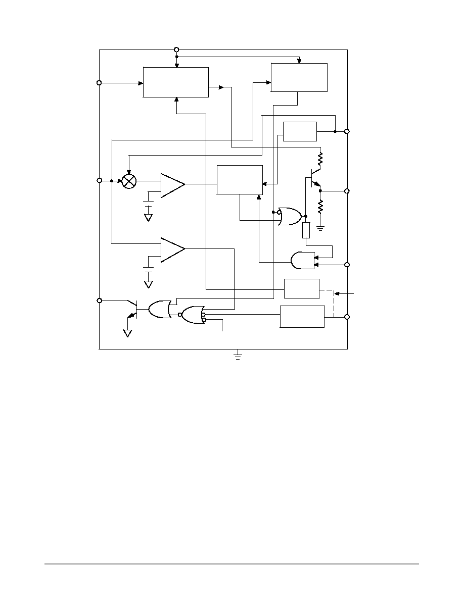
Figure 1. Block Diagram
IGN
Sense
LAMP
V
CC
V
SUP
GND
STATOR
ENABLE
DELAY
Lamp
Indicator
S
R
Q
R
STATOR
Timer
V
HV
V
REG
+
≠
ENABLE
Series
Regulator
Load Dump
Detection and
Protection
V
SUP
RS Flop
Set
Dominate
Power Up
STATOR
OSC
Device Driver
SC
Note:
CS3341/CS387
Disconnected
CS3351 Connected
OSC
+
≠
+
Regulator
Comparator
High Voltage
Comparator
+

CS3341, CS3351, CS387
http://onsemi.com
3
MAXIMUM RATINGS*
Rating
Value
Unit
Storage Temperature Range, T
S
≠55 to +165
∞
C
Junction Temperature Range
≠40 to 150
∞
C
Continuous Supply
27
V
I
CC
Load Dump
400
mA
Lead Temperature Soldering:
Reflow: (SMD styles only) (Note 1)
230 peak
∞
C
1. 60 second maximum above 183
∞
C.
*The maximum package power dissipation must be observed.
ELECTRICAL CHARACTERISTICS
(≠40
∞
C < T
A
< 125
∞
C, ≠40
∞
C < T
J
< 150
∞
C, 9.0 V
V
CC
17 V; unless otherwise
specified.)
Characteristic
Test Conditions
Min
Typ
Max
Unit
Supply
Supply Current Enabled
≠
≠
12
25
mA
Supply Current Disabled
≠
≠
≠
50
µ
A
Driver Stage
Output High Current
V
DD
= 1.2 V
≠10
≠6.0
≠4.0
mA
Output Low Voltage
I
OL
= 25
µ
A
≠
≠
0.35
V
Minimum ON Time
≠
200
≠
≠
µ
s
Minimum Duty Cycle
≠
≠
6.0
10
%
Short Circuit Duty Cycle
≠
1.0
≠
5.0
%
Field Switch Turn On
Rise Time
≠
30
≠
90
µ
s
Field Switch Turn On
Fall Time
≠
30
≠
90
µ
s
Stator
Input High Voltage
≠
10
≠
≠
V
Input Low Voltage
≠
≠
≠
6.0
V
Stator Time Out
High to Low
6.0
100
600
ms
Stator Power≠Up Input High
CS3351 only
10
≠
≠
V
Stator Power≠Up Input Low
CS3351 only
≠
≠
6.0
V
Lamp
Output High Current
V
LAMP
@
3.0 V
≠
≠
50
µ
A
Output Low Voltage
I
LAMP
@ 30 mA
≠
≠
0.35
V
Ignition
Input High Voltage
I
CC
> 1.0 mA
1.8
≠
≠
V
Input Low Voltage
I
CC
< 100
µ
A
≠
≠
0.5
V
Oscillator
Oscillator Frequency
C
OSC
= 0.22
µ
F
65
≠
325
Hz
Rise Time/Fall Time
C
OSC
= 0.22
µ
F
≠
17
≠
≠
Oscillator High Threshold
C
OSC
= 0.22
µ
F
≠
≠
6.0
V
CS3341, CS3351, CS387
http://onsemi.com
4
ELECTRICAL CHARACTERISTICS (continued)
(≠40
∞
C < T
A
< 125
∞
C, ≠40
∞
C < T
J
< 150
∞
C, 9.0 V
V
CC
17 V; unless otherwise
specified.)
Characteristic
Unit
Max
Typ
Min
Test Conditions
Battery Sense
Input Current
≠
≠10
≠
+10
µ
A
Regulation Voltage
@25
∞
C, R
1
= 100 k
, R
2
= 50 k
13.5
≠
16
V
Proportional Control
≠
0.050
≠
0.400
V
High Voltage Threshold Ratio
VHigh Voltage @ LampOn
VRegulation @ 50%Duty Cycle
1.083
≠
1.190
≠
High Voltage Hysteresis
≠
0.020
≠
0.600
V
PACKAGE PIN DESCRIPTION
PACKAGE PIN #
SO≠14
Flip Chip
PIN SYMBOL
FUNCTION
1
1
Driver
Output driver for external power switch≠Darlington.
2
2
GND
Ground.
3, 6, 7, 9, 13
3
NC
No Connection.
4
4
OSC
Timing capacitor for oscillator.
5
5
Lamp
Base driver for lamp driver indicates no stator signal or overvoltage condition.
8
6
IGN
Switched ignition power up.
10
7
Stator
Stator signal input for stator timer (CS3351 also power up).
11
8
Sense
Battery sense voltage regulator comparator input and protection.
12
9
V
CC
Supply for IC.
14
10
SC
Short circuit sensing.
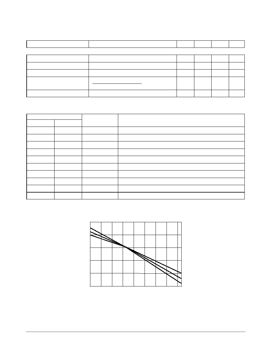
TYPICAL PERFORMANCE CHARACTERISTICS
Figure 2. Battery Voltage vs. Temperature (
∞
C)
Over Process Variation
15.5
15
14.5
14
13.5
13
≠40
≠20
0
20
40
60
80
100
120
Temperature (
∞
C)
Battery V
oltage
CS3341, CS3351, CS387
http://onsemi.com
5
APPLICATIONS INFORMATION
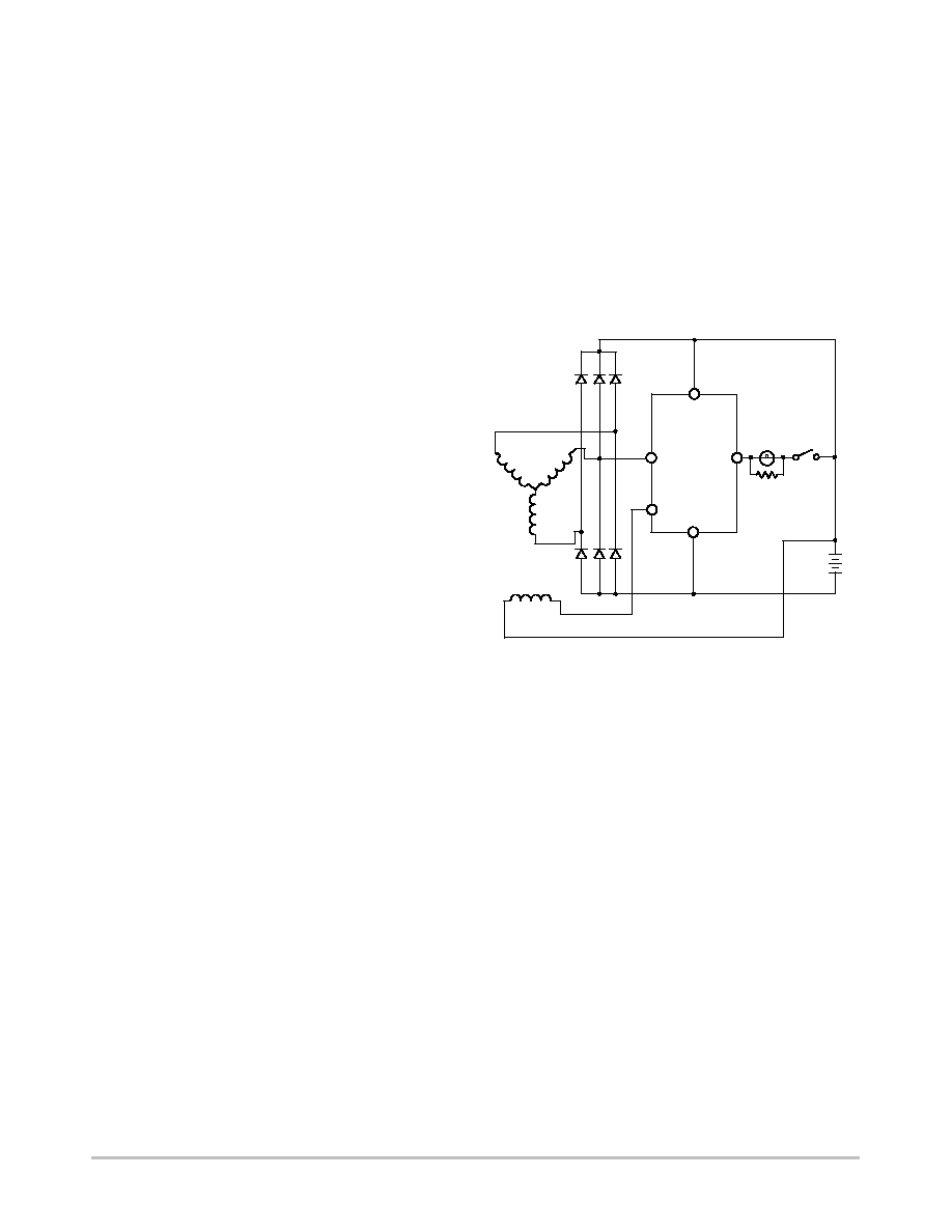
The CS3341 and CS3351 IC's are designed for use in an
alternator charging system. The circuit is also available in
flip≠chip form as the CS387.
In a standard alternator design (Figure 3), the rotor carries
the field winding. An alternator rotor usually has several N
and S poles. The magnetic field for the rotor is produced by
forcing current through a field or rotor winding. The Stator
windings are formed into a number of coils spaced around
a cylindrical core. The number of coils equals the number of
pairs of N and S poles on the rotor. The alternating current
in the Stator windings is rectified by the diodes and applied
to the regulator. By controlling the amount of field current,
the magnetic field strength is controlled and hence the
output voltage of the alternator.
Referring to Figure 7, a typical application diagram, the
oscillator frequency is set by an external capacitor
connected between OSC and ground. The sawtooth
waveform ramps between 1.0 V and 3.0 V and provides the
timing for the system. For the circuit shown the oscillator
frequency is approximately 140 Hz. The alternator voltage
is sensed at Terminal A via the resistor divider network
R1/R2 on the Sense pin of the IC. The voltage at the sense
pin determines the duty cycle for the regulator. The voltage
is adjusted by potentiometer R2. A relatively low voltage on
the sense pin causes a long duty cycle that increases the Field
current. A high voltage results in a short duty cycle.
The ignition Terminal (I) switches power to the IC
through the V
CC
pin. In the CS3351 the Stator pin senses the
voltage from the stator. This will keep the device powered
while the voltage is high, and it also senses a stopped engine
condition and drives the Lamp pin high after the stator
timeout expires. The Lamp pin also goes high when an
overvoltage condition is detected on the sense pin. This
causes the darlington lamp drive transistor to switch on and
pull current through the lamp. If the system voltage
continues to increase, the field and lamp output turn off as
in an overvoltage or load dump condition.
The SC or Short Circuit pin monitors the field voltage. If
the drive output and the SC voltage are simultaneously high
for a predetermined period, a short circuit condition is
assumed and the output is disabled. The regulator is forced
to a minimum short circuit duty cycle.
Figure 3. IAR System Block Diagram
BATT
Ignition
Switch
Regulator
A
GND
I
S
FIELD
FIELD
Winding
STATOR
Winding
Lamp
Indicator
CS3341, CS3351, CS387
http://onsemi.com
6
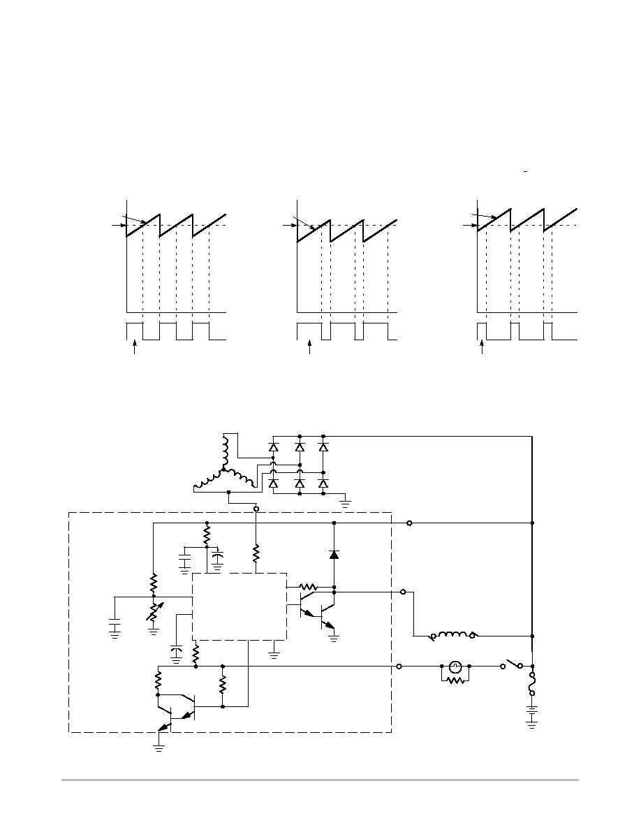
REGULATION WAVEFORMS
The CS3341/3351/387 utilizes proportion control to
maintain regulation. Waveforms depicting operation are
shown in Figures 4, 5 and 6, where V
BAT/N
is the divided
down voltage present on the Sense pin using R1 and R2
(Figure 7). A sawtooth waveform is generated internally.
The amplitude of this waveform is listed in the electric
parameter section as proportion control. The oscillator
voltage is summed with V
BAT/N
, and compared with the
internal voltage regulator (V
REG
) in the regulation
comparator which controls the field through the output
"Device Driver."
Figure 4 shows typical steady≠state operation. A 50%
duty cycle is maintained.
Figure 5 shows the effect of a drop in voltage on (V
BAT/N
+ V
OSC
). Notice the duty cycle increase to the field drive.
Figure 6 shows the effect of an increase in voltage (above
the regulation voltage) on (V
BAT/N
+ V
OSC
). Notice the
decrease in field drive.
ŒŒ
ŒŒ
ŒŒŒ
ŒŒŒ
ŒŒ
ŒŒ
Figure 4. 50% Duty Cycle,
Steady State
Figure 5. > 50% Duty Cycle,
Increased Load
Figure 6. < 50% Duty Cycle,
Decreased Load
V
REG
V
BAT/N
+ V
OSC
V
REG
V
REG
V
BAT/N
+ V
OSC
Field Driver On
Field Driver On
Field Driver On
V
BAT/N
+ V
OSC
Figure 7. Typical Application DIagram
D1
C3
BATTERY
2N6284
Power
Darlington
POWER GROUND
R4
18 k
C1
0.1
µ
F
R2
50 k
0.047
µ
F
C4
0.022
µ
F
R6
20 k
R9
2.4 k
GND
Driver
SC
STATOR
STATOR
RECTIFIER
S
A
F
I
FIELD
Lamp Indicator
R10
510
IGNITION
SWITCH
R7
MPSA13
or CS299
*Note: C2 optional for reduced jitter.
LAMP
V
CC
Sense
OSC
IGN
*C2
10
µ
F
R1
100 k
R5 10 k
R3
250
10
MR2502
MR2502
MR2502
CS3341, CS3351, CS387
http://onsemi.com
7
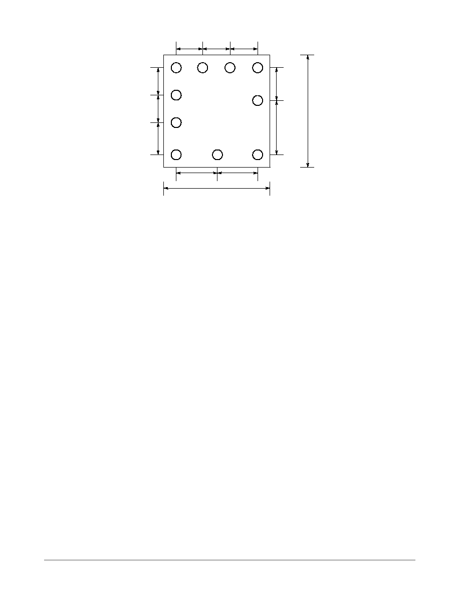
488
µ
m
506
µ
m
510
µ
m
762
µ
m
742
µ
m
1.96 mm
506
µ
m
506
µ
m
594
µ
m
605
µ
m
1000
µ
m
2.07 mm
Figure 8. Flip Chip Dimensions and Solder Bump Locations, Bump Side Up
CS3341, CS3351, CS387
http://onsemi.com
8
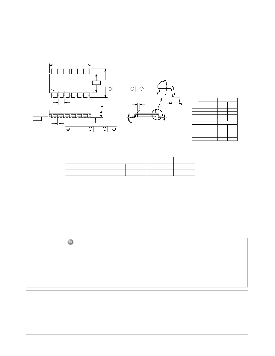
PACKAGE DIMENSIONS
NOTES:
1. DIMENSIONING AND TOLERANCING PER ANSI
Y14.5M, 1982.
2. CONTROLLING DIMENSION: MILLIMETER.
3. DIMENSIONS A AND B DO NOT INCLUDE
MOLD PROTRUSION.
4. MAXIMUM MOLD PROTRUSION 0.15 (0.006)
PER SIDE.
5. DIMENSION D DOES NOT INCLUDE DAMBAR
PROTRUSION. ALLOWABLE DAMBAR
PROTRUSION SHALL BE 0.127 (0.005) TOTAL
IN EXCESS OF THE D DIMENSION AT
MAXIMUM MATERIAL CONDITION.
≠A≠
≠B≠
G
P
7 PL
14
8
7
1
M
0.25 (0.010)
B
M
S
B
M
0.25 (0.010)
A
S
T
≠T≠
F
R
X 45
SEATING
PLANE
D
14 PL
K
C
J
M
_
DIM
MIN
MAX
MIN
MAX
INCHES
MILLIMETERS
A
8.55
8.75
0.337
0.344
B
3.80
4.00
0.150
0.157
C
1.35
1.75
0.054
0.068
D
0.35
0.49
0.014
0.019
F
0.40
1.25
0.016
0.049
G
1.27 BSC
0.050 BSC
J
0.19
0.25
0.008
0.009
K
0.10
0.25
0.004
0.009
M
0
7
0
7
P
5.80
6.20
0.228
0.244
R
0.25
0.50
0.010
0.019
_
_
_
_
SO≠14
D SUFFIX
CASE 751A≠03
ISSUE F
PACKAGE THERMAL DATA
Parameter
SO≠14
Unit
R
JC
Typical
30
∞
C/W
R
JA
Typical
125
∞
C/W
ON Semiconductor and are registered trademarks of Semiconductor Components Industries, LLC (SCILLC). SCILLC reserves the right to make
changes without further notice to any products herein. SCILLC makes no warranty, representation or guarantee regarding the suitability of its products for any
particular purpose, nor does SCILLC assume any liability arising out of the application or use of any product or circuit, and specifically disclaims any and all
liability, including without limitation special, consequential or incidental damages. "Typical" parameters which may be provided in SCILLC data sheets and/or
specifications can and do vary in different applications and actual performance may vary over time. All operating parameters, including "Typicals" must be
validated for each customer application by customer's technical experts. SCILLC does not convey any license under its patent rights nor the rights of others.
SCILLC products are not designed, intended, or authorized for use as components in systems intended for surgical implant into the body, or other applications
intended to support or sustain life, or for any other application in which the failure of the SCILLC product could create a situation where personal injury or death
may occur. Should Buyer purchase or use SCILLC products for any such unintended or unauthorized application, Buyer shall indemnify and hold SCILLC
and its officers, employees, subsidiaries, affiliates, and distributors harmless against all claims, costs, damages, and expenses, and reasonable attorney fees
arising out of, directly or indirectly, any claim of personal injury or death associated with such unintended or unauthorized use, even if such claim alleges that
SCILLC was negligent regarding the design or manufacture of the part. SCILLC is an Equal Opportunity/Affirmative Action Employer.
PUBLICATION ORDERING INFORMATION
JAPAN: ON Semiconductor, Japan Customer Focus Center
2≠9≠1 Kamimeguro, Meguro≠ku, Tokyo, Japan 153≠0051
Phone: 81≠3≠5773≠3850
Email: r14525@onsemi.com
ON Semiconductor Website: http://onsemi.com
For additional information, please contact your local
Sales Representative.
CS3341/D
Literature Fulfillment:
Literature Distribution Center for ON Semiconductor
P.O. Box 5163, Denver, Colorado 80217 USA
Phone: 303≠675≠2175 or 800≠344≠3860 Toll Free USA/Canada
Fax: 303≠675≠2176 or 800≠344≠3867 Toll Free USA/Canada
Email: ONlit@hibbertco.com
N. American Technical Support: 800≠282≠9855 Toll Free USA/Canada