
©
Semiconductor Components Industries, LLC, 2004
January, 2004 - Rev. 9
1
Publication Order Number:
CS5204-2/D
CS5204-2
4.0 A, 1.5 V Fixed Linear
Regulator
The CS5204-2 linear regulator provides 4.0 A @ 1.5 V with an
accuracy of
±
2.0%.
The fast loop response and low dropout voltage make this regulator
ideal for GTL bus termination where low voltage operation and good
transient response are important.
The circuit is designed to operate with dropout voltages as low as 1.0 V
depending on the output current level. The maximum quiescent current is
only 10 mA at full load.
The regulator is fully protected against overload conditions with
protection circuitry for Safe Operating Area (SOA), overcurrent and
thermal shutdown.
The regulator is available in TO-220-3 and surface mount D
2
PAK-3
packages.
Features
∑
Output Current to 4.0 A
∑
Output Voltage Trimmed to
±
2.0%
∑
Dropout Voltage (typical) 1.10 V @ 4.0 A
∑
Fast Transient Response
∑
Fault Protection Circuitry
-
Thermal Shutdown
-
Overcurrent Protection
-
Safe Area Protection
Figure 1. Block Diagram
+
-
Thermal
Shutdown
Bandgap
Output
Current
Limit
Error
Amplifier
V
OUT
GND
V
IN
D
2
PAK-3
D2T SUFFIX
CASE 418AB
TO-220-3
T SUFFIX
CASE 221A
1
2
3
Tab = V
OUT
Pin 1. GND
2. V
OUT
3. V
IN
MARKING DIAGRAMS
CS5204-2
AWLYWW
1
CS5204-2
AWLYWW
1
D
2
PAK-3
TO-220-3
A
= Assembly Location
WL, L
= Wafer Lot
YY, Y
= Year
WW, W = Work Week
1
2
3
http://onsemi.com
See detailed ordering and shipping information in the package
dimensions section on page 5 of this data sheet.
ORDERING INFORMATION
CS5204-2
http://onsemi.com
2
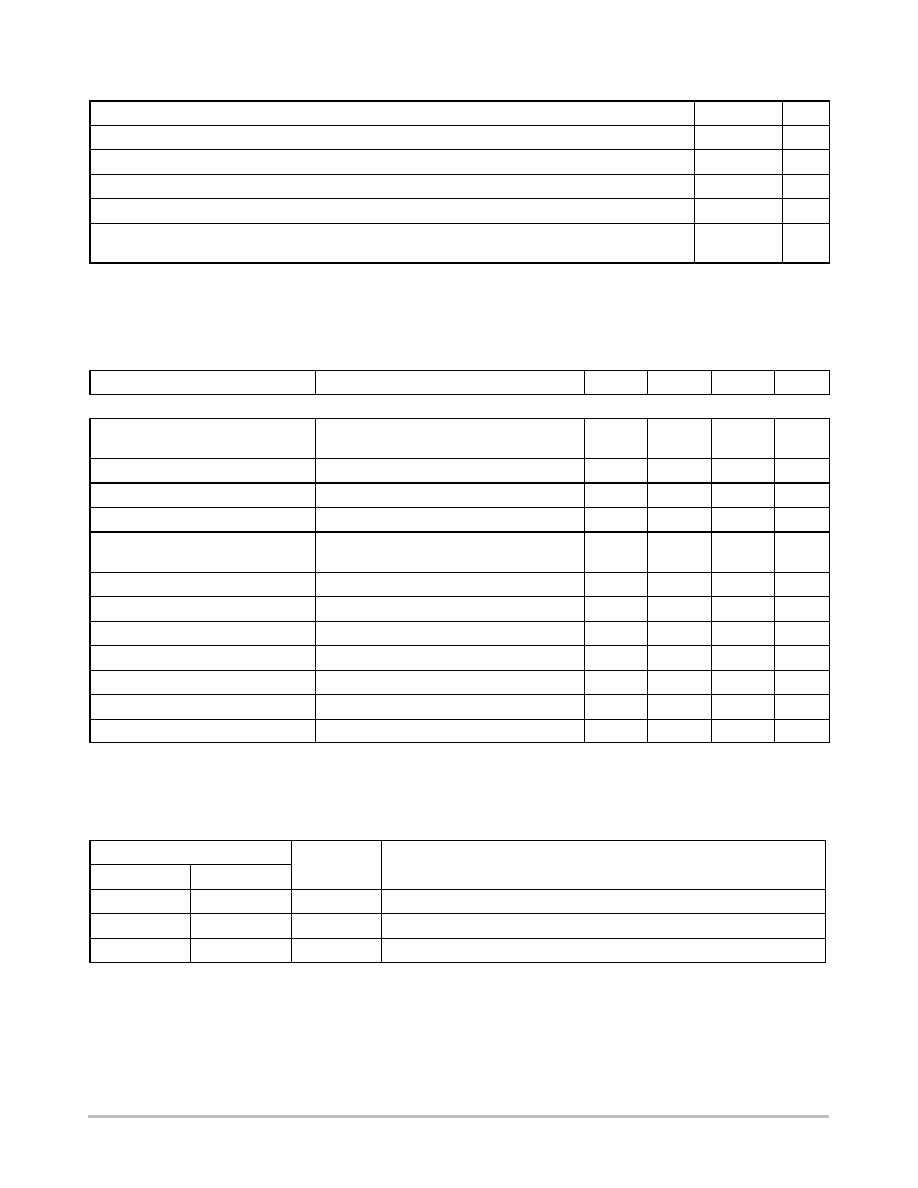
MAXIMUM RATINGS*
Parameter
Value
Unit
Supply Voltage, V
CC
17
V
Operating Temperature Range
-40 to +70
∞
C
Junction Temperature
150
∞
C
Storage Temperature Range
-60 to +150
∞
C
Lead Temperature Soldering:
Wave Solder (through hole styles only) Note 1
Reflow (SMD styles only) Note 2
260 Peak
230 Peak
∞
C
∞
C
1. 10 second maximum.
2. 60 second maximum above 183
∞
C
*The maximum package power dissipation must be observed.
ELECTRICAL CHARACTERISTICS
(C
IN
= 10
m
F, C
OUT
= 22
m
F Tantalum, V
IN
- V
OUT
= 3.0 V, V
IN
10 V, 0
∞
C
T
A
70
∞
C,
T
J
+150
∞
C, unless otherwise specified, I
full load
= 4.0 A)
Characteristic
Test Conditions
Min
Typ
Max
Unit
CS5204-2
Output Voltage (Notes 3 and 4)
V
IN
- V
OUT
= 1.5 V;
0
I
OUT
4.0 A
1.47
(-2.0%)
1.50
1.53
(+2.0%)
V
Line Regulation
1.5 V
V
IN
- V
OUT
6.0 V; I
OUT
= 10 mA
-
0.04
0.20
%
Load Regulation (Notes 3 and 4)
V
IN
- V
OUT
= 1.5 V; 10 mA
I
OUT
4.0 A
-
0.05
0.4
%
Dropout Voltage (Note 5)
I
OUT
= 4.0 A
-
1.1
1.2
V
Current Limit
V
IN
- V
OUT
= 3.0 V; T
J
25
∞
C
V
IN
- V
OUT
= 15 V
4.5
-
8.5
2.5
-
-
A
A
Quiescent Current
V
IN
9.0 V; I
OUT
= 10 mA
-
5.0
10
mA
Thermal Regulation
30 ms Pulse, T
A
= 25
∞
C
-
0.003
-
%/W
Ripple Rejection
f = 120 Hz; I
OUT
= 4.0 A
-
75
-
dB
Temperature Stability
-
-
0.5
-
%
RMS Output Noise (%V
OUT
)
10 Hz
f
10 kHz
-
0.003
-
%/V
OUT
Thermal Shutdown
-
150
180
-
∞
C
Thermal Shutdown Hysteresis
-
-
25
-
∞
C
3. Load regulation and output voltage are measured at a constant junction temperature by low duty cycle pulse testing. Changes in output
voltage due to thermal gradients or temperature changes must be taken into account separately.
4. Specifications apply for an external Kelvin sense connection at a point on the output pin 1/4" from the bottom of the package.
5. Dropout voltage is a measurement of the minimum input/output differential at full load.
PACKAGE PIN DESCRIPTION
Package Pin Number
TO-220-3
D
2
PAK-3
Pin Symbol
Function
1
1
GND
Ground connection.
2
2
V
OUT
Regulated output voltage (case).
3
3
V
IN
Input voltage.
CS5204-2
http://onsemi.com
3
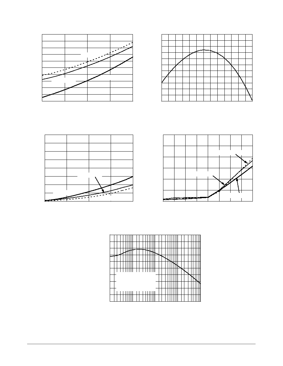
TYPICAL PERFORMANCE CHARACTERISTICS
Figure 2. Dropout Voltage vs. Output
Current
Figure 3. Reference Voltage vs.
Temperature
Figure 4. Load Regulation vs.
Output Current
Figure 5. Minimum Load Current
Figure 6. Ripple Rejection vs. Frequency
T
J
(
∞
C)
0.10
10
Output V
oltage Deviation (%)
0.08
0.06
0.04
0.02
0.00
-0.02
-0.04
-0.06
-0.08
-0.10
-0.12
0
20 30
40 50
60 70
80 90 100 110 120 130
V
IN
- V
OUT
(V)
2.500
Minimum Load Current (mA)
1
2.175
1.850
1.525
1.200
0.875
0.550
2
3
4
5
6
7
8
9
T
CASE
= 125
∞
C
T
CASE
= 25
∞
C
T
CASE
= 0
∞
C
Frequency (Hz)
Ripple Rejection (dB)
10
1
100
90
80
70
60
50
40
30
20
10
0
10
2
10
3
10
4
10
5
T
CASE
= 25
∞
C
I
OUT
= 4.0 A
(V
IN
- V
OUT
) = 3.0 V
V
RIPPLE
= 1.6 V
PP
0
1
2
3
4
T
CASE
= 0
∞
C
T
CASE
= 125
∞
C
T
CASE
= 25
∞
C
1.20
1.15
1.10
1.05
1.00
0.95
0.90
0.85
0.80
0.75
0.70
Dropout
V
oltage (V)
Output Current (A)
Output Current (A)
Output V
oltage Deviation (%)
0.200
0
0.175
0.150
0.125
0.100
0.075
0.050
0.025
0.000
1
2
3
4
T
CASE
= 25
∞
C
T
CASE
= 125
∞
C
T
CASE
= 0
∞
C

CS5204-2
http://onsemi.com
4
APPLICATIONS INFORMATION
The CS5204-2 linear regulator provides fixed 1.5 V
voltage at currents up to 4.0 A. The regulator is protected
against short circuit, and includes thermal shutdown and
safe area protection (SOA) circuitry. The SOA protection
circuitry decreases the maximum available output current as
the input-output differential voltage increase.
The CS5204-2 has a composite PNP-NPN output
transistor and requires an output capacitor for stability. A
detailed procedure for selecting this capacitor is included in
the Stability Considerations section.
Stability Considerations
The output compensation capacitor helps determine three
main characteristics of a linear regulator: start-up delay,
load transient response, and loop stability.
The capacitor value and type is based on cost, availability,
size and temperature constraints. A tantalum or aluminum
electrolytic capacitor is best, since a film or ceramic
capacitor with almost zero ESR can cause instability. The
aluminum electrolytic capacitor is the least expensive
solution. However, when the circuit operates at low
temperatures, both the value and ESR of the capacitor will
vary considerably. The capacitor manufacturer's data sheet
provides this information.
A 22
mF tantalum capacitor will work for most
applications, but with high current regulators such as the
CS5204-2 the transient response and stability improve with
higher values of capacitance. The majority of applications
for this regulator involve large changes in load current so the
output capacitor must supply the instantaneous load current.
The ESR of the output capacitor causes an immediate drop
in output voltage given by:
D
V
+ D
I
ESR
For microprocessor applications it is customary to use an
output capacitor network consisting of several tantalum and
ceramic capacitors in parallel. This reduces the overall ESR
and reduces the instantaneous output voltage drop under
transient load conditions. The output capacitor network
should be as close to the load as possible for the best results.
Protection Diodes
When large external capacitors are used with a linear
regulator it is sometimes necessary to add protection diodes.
If the input voltage of the regulator gets shorted, the output
capacitor will discharge into the output of the regulator. The
discharge current depends on the value of the capacitor, the
output voltage and the rate at which V
IN
drops. In the
CS5204-2 linear regulator, the discharge path is through a
large junction and protection diodes are not usually needed.
If the regulator is used with large values of output
capacitance and the input voltage is instantaneously shorted
to ground, damage can occur. In this case, a diode connected
as shown in Figure 7 is recommended.
Figure 7. Protection Diode Scheme
V
IN
CS5204-2
V
OUT
GND
V
OUT
V
IN
C
1
C
2
IN4002 (Optional)
Output Voltage Sensing
Since the CS5204-2 is a three terminal regulator, it is not
possible to provide true remote load sensing. Load
regulation is limited by the resistance of the conductors
connecting the regulator to the load. For best results the
regulator should be connected as shown in Figure 8.
Figure 8. Conductor Parasitic Resistance Effects Can
Be Minimized With the Above Grounding Scheme
V
IN
V
IN
V
OUT
CS5204-2
Conductor Parasitic
Resistance
R
LOAD
R
C
GND
CS5204-2
http://onsemi.com
5
Calculating Power Dissipation and Heat Sink
Requirements
The CS5204-2 linear regulator includes thermal
shutdown and safe operating area circuitry to protect the
device. High power regulators such as these usually operate
at high junction temperatures so it is important to calculate
the power dissipation and junction temperatures accurately
to ensure that an adequate heat sink is used.
The case is connected to V
OUT
on the CS5204-2,
electrical isolation may be required for some applications.
Thermal compound should always be used with high current
regulators such as these.
The thermal characteristics of an IC depend on the
following four factors:
1.
Maximum Ambient Temperature T
A
(
∞
C)
2.
Power dissipation P
D
(Watts)
3.
Maximum junction temperature T
J
(
∞
C)
4.
Thermal resistance junction to ambient R
qJA
(
∞
C/W)
These four are related by the equation
TJ
+
TA
)
PD
R
Q
JA
(1)
The maximum ambient temperature and the power
dissipation are determined by the design while the
maximum junction temperature and the thermal resistance
depend on the manufacturer and the package type.
The maximum power dissipation for a regulator is:
PD(max)
+
{VIN(max)
*
VOUT(min)}IOUT(max)
)
VIN(max)IQ
(2)
where:
V
IN(max)
is the maximum input voltage,
V
OUT(min)
is the minimum output voltage,
I
OUT(max)
is the maximum output current, for the
application
I
Q
is the maximum quiescent current at I
OUT(max)
.
A heat sink effectively increases the surface area of the
package to improve the flow of heat away from the IC and
into the surrounding air.
Each material in the heat flow path between the IC and the
outside environment has a thermal resistance. Like series
electrical resistances, these resistances are summed to
determine R
qJA
, the total thermal resistance between the
junction and the surrounding air.
1.
Thermal Resistance of the junction to case, R
qJC
(
∞
C/W)
2.
Thermal Resistance of the case to Heat Sink, R
qCS
(
∞
C/W)
3.
Thermal Resistance of the Heat Sink to the ambient
air, R
qSA
(
∞
C/W)
These are connected by the equation:
R
Q
JA
+
R
Q
JC
)
R
Q
CS
)
R
Q
SA
(3)
The value for R
qJA
is calculated using equation (3) and the
result can be substituted in equation (1).
R
qJC
is 1.6
∞
C/Watt for the CS5204-2. For a high current
regulator such as the CS5204-2 the majority of the heat is
generated in the power transistor section. The value for R
qSA
depends on the heat sink type, while R
qCS
depends on
factors such as package type, heat sink interface (is an
insulator and thermal grease used?), and the contact area
between the heat sink and the package. Once these
calculations are complete, the maximum permissible value
of R
qJA
can be calculated and the proper heat sink selected.
For further discussion on heat sink selection, see application
note "Thermal Management," document number
AND8036/D, available through the Literature Distribution
Center or via our website at http://onsemi.com.
ORDERING INFORMATION
Orderable Part Number
Type
Package
Shipping
CS5204-2GT3
4.0 A, 1.5 V Output
TO-220-3, STRAIGHT
50 Units / Rail
CS5204-2GDP3
4.0 A, 1.5 V Output
D
2
PAK-3
50 Units / Rail
CS5204-2GDPR3
4.0 A, 1.5 V Output
D
2
PAK-3
750 / Tape & Reel
For information on tape and reel specifications, including part orientation and tape sizes, please refer to our Tape and Reel Packaging
Specifications Brochure, BRD8011/D.
CS5204-2
http://onsemi.com
6
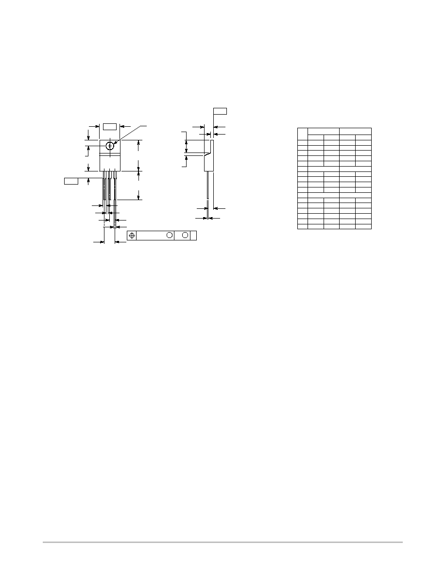
PACKAGE DIMENSIONS
TO-220-3
T SUFFIX
CASE 221A-08
ISSUE AA
NOTES:
1. DIMENSIONING AND TOLERANCING PER ANSI
Y14.5M, 1982.
2. CONTROLLING DIMENSION: INCH.
A
K
L
G
D
N
H
Q
F
1 2 3
4
-T-
SEATING
PLANE
S
R
J
U
T
C
3 PL
-B-
-Y-
M
B
M
0.25 (0.010)
Y
DIM
MIN
MAX
MIN
MAX
MILLIMETERS
INCHES
A
0.560
0.625
14.23
15.87
B
0.380
0.420
9.66
10.66
C
0.140
0.190
3.56
4.82
D
0.025
0.035
0.64
0.89
F
0.139
0.155
3.53
3.93
G
0.100 BSC
2.54 BSC
H
---
0.280
---
7.11
J
0.012
0.045
0.31
1.14
K
0.500
0.580
12.70
14.73
L
0.045
0.060
1.15
1.52
N
0.200 BSC
5.08 BSC
Q
0.100
0.135
2.54
3.42
R
0.080
0.115
2.04
2.92
S
0.020
0.055
0.51
1.39
T
0.235
0.255
5.97
6.47
U
0.000
0.050
0.00
1.27
V
V
0.045
---
1.15
---

CS5204-2
http://onsemi.com
7
PACKAGE DIMENSIONS
D
2
PAK-3
DP SUFFIX
CASE 418AB-01
ISSUE O
For D
2
PAK Outline and
Dimensions - Contact Factory
PACKAGE THERMAL DATA
Parameter
TO-220-3
D
2
PAK-3
Unit
R
q
JC
Typical
1.6
1.6
∞
C/W
R
q
JA
Typical
50
10-50*
∞
C/W
*Depending on thermal properties of substrate. R
q
JA
=
R
q
JC
+
R
q
CA
CS5204-2
http://onsemi.com
8
ON Semiconductor and are registered trademarks of Semiconductor Components Industries, LLC (SCILLC). SCILLC reserves the right to make changes without further notice
to any products herein. SCILLC makes no warranty, representation or guarantee regarding the suitability of its products for any particular purpose, nor does SCILLC assume any liability
arising out of the application or use of any product or circuit, and specifically disclaims any and all liability, including without limitation special, consequential or incidental damages.
"Typical" parameters which may be provided in SCILLC data sheets and/or specifications can and do vary in different applications and actual performance may vary over time. All
operating parameters, including "Typicals" must be validated for each customer application by customer's technical experts. SCILLC does not convey any license under its patent rights
nor the rights of others. SCILLC products are not designed, intended, or authorized for use as components in systems intended for surgical implant into the body, or other applications
intended to support or sustain life, or for any other application in which the failure of the SCILLC product could create a situation where personal injury or death may occur. Should
Buyer purchase or use SCILLC products for any such unintended or unauthorized application, Buyer shall indemnify and hold SCILLC and its officers, employees, subsidiaries, affiliates,
and distributors harmless against all claims, costs, damages, and expenses, and reasonable attorney fees arising out of, directly or indirectly, any claim of personal injury or death
associated with such unintended or unauthorized use, even if such claim alleges that SCILLC was negligent regarding the design or manufacture of the part. SCILLC is an Equal
Opportunity/Affirmative Action Employer. This literature is subject to all applicable copyright laws and is not for resale in any manner.
PUBLICATION ORDERING INFORMATION
N. American Technical Support: 800-282-9855 Toll Free
USA/Canada
Japan: ON Semiconductor, Japan Customer Focus Center
2-9-1 Kamimeguro, Meguro-ku, Tokyo, Japan 153-0051
Phone: 81-3-5773-3850
CS5204-2/D
LITERATURE FULFILLMENT:
Literature Distribution Center for ON Semiconductor
P.O. Box 5163, Denver, Colorado 80217 USA
Phone: 303-675-2175 or 800-344-3860 Toll Free USA/Canada
Fax: 303-675-2176 or 800-344-3867 Toll Free USA/Canada
Email: orderlit@onsemi.com
ON Semiconductor Website: http://onsemi.com
Order Literature: http://www.onsemi.com/litorder
For additional information, please contact your
local Sales Representative.