©
Semiconductor Components Industries, LLC, 2002
May, 2002 ≠ Rev. 2
1
Publication Order Number:
CS5212/D
CS5212
Low Voltage Synchronous
Buck Controller
The CS5212 is a low voltage synchronous buck controller. It
contains all required circuitry for a synchronous buck converter using
external N≠Channel MOSFETs. High current internal gate drivers are
capable of driving high gate capacitance of low R
DS(on)
NFETs for
better efficiency. The V
2
TM
control architecture is used to achieve
unmatched transient response, the best overall regulation and the
simplest loop compensation.
Additionally, the CS5212 provides overcurrent protection,
undervoltage lockout, soft start, built≠in adaptive non≠overlap, and an
adjustable fixed frequency range of 150 kHz to 750 kHz, which gives
the designer more flexibility to make efficiency and component size
trade offs. The CS5212 will also operate over a 3.1 V to 7.0 V range
using either single or dual input voltage.
Features
∑
Switching Regulator Controller
≠
N≠Channel Synchronous Buck Design
≠
V
2
Control Topology
≠
200 ns Transient Response
≠
Programmable Fixed Frequency of 150 kHz≠750 kHz
≠
1.0 V 1.5% Internal Reference
≠
Lossless Inductor Sensing Overcurrent Protection
≠
Hiccup Mode Short Circuit Protection
≠
Programmable Soft Start
≠
40 ns GATE Rise and Fall Times (3.3 nF Load)
≠
70 ns Adaptive FET Nonoverlap Time
≠
Differential Remote Sense Capability
≠
Available in Industrial and Commerical Temperature Grades
∑
System Power Management
≠
3.3 V Operation
≠
Undervoltage Lockout
≠
On/Off Control Through Use of the COMP Pin
MARKING
DIAGRAM
x
= E or G
A
= Assembly Location
WL, L
= Wafer Lot
YY, Y
= Year
WW, W
= Work Week
1
GATE(L)
PGND
SGND
V
FB
GATE(H)
IS+
IS≠
R
OSC
V
CC
PIN CONNECTIONS
V
C
BST
LGND
V
FFB
COMP
SOIC≠14
D SUFFIX
CASE 751A
1
14
CS5212x
AWLYWW
See detailed ordering and shipping information in the package
dimensions section on page 13 of this data sheet.
ORDERING INFORMATION
http://onsemi.com
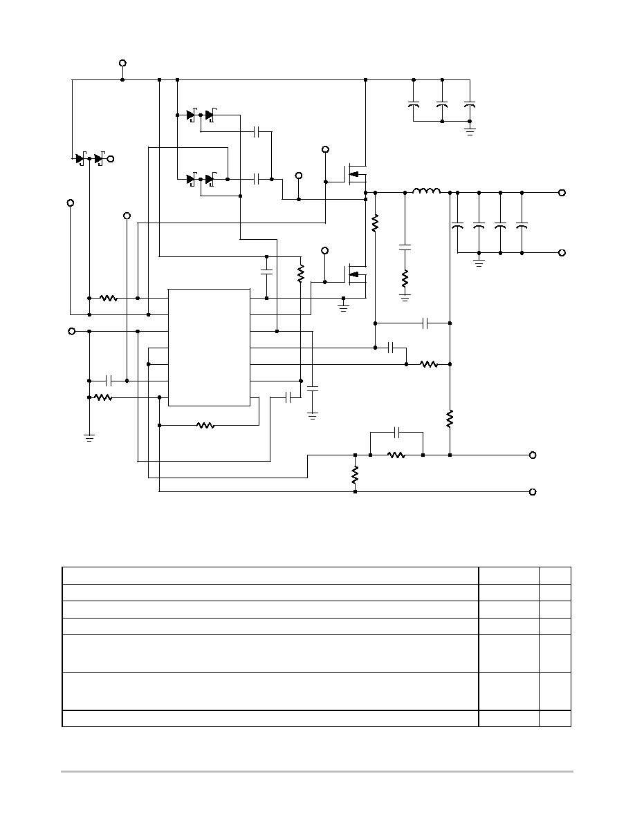
CS5212
http://onsemi.com
2
C16
0.1
µ
F
GATE(H)
BST
LGND
V
FFB
V
FB
COMP
SGND
PGND
GATE(L)
V
C
IS+
IS≠
V
CC
R
OSC
CS5212
U1
GN2
GND
R8
10
C2
0.1
µ
F
TP4
COMP
TP5
BST
1
2
3
4
5
6
7
14
13
12
11
10
9
8
C11
0.1
µ
F
R1
51 k
C1
0.47
µ
F
R9
10
C19
1.0
µ
F
Q2
Q1
TP3
GATE(L)
TP2
GATE(H)
TP1
SWNODE
V
IN
3.3 V
D5
BAT54S
+
+
+
C6
C7
C8 100
µ
F/10 V
◊
3
R5
4.7 k
R13
10
C15
470 pF
L1
2.9
µ
H
6.5 mR
ETQP6F2R9LB
V
OUT
GND
C3
0.1
µ
F
R6
4.7 k
R2
10
TP6
SENSE+
TP7
SENSE≠
R4
1.0 k 1%
C5
680 pF
R3
1.5 k 1%
R7
TBD*
D6
BAT54S
D2
BAT54S
C4
0.1
µ
F
C22
0.1
µ
F
*Refer to Rpullup Value Selection section for value needed.
+
C9
+
C10
100
µ
F/10 V
◊
2
+
C20
+
C21
Figure 1. Application Diagram, 3.3 V to 1.5 V/8.0 A Converter with Differential Remote Sense
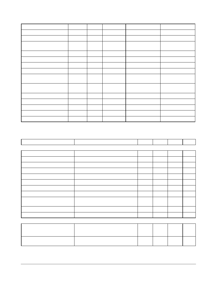
MAXIMUM RATINGS*
Rating
Value
Unit
Operating Junction Temperature, T
J
150
∞
C
Lead Temperature Soldering:
Reflow: (SMD styles only) (Note 1)
230 peak
∞
C
Storage Temperature Range, T
S
≠65 to +150
∞
C
Package Thermal Resistance:
Junction≠to≠Case, R
JC
Junction≠to≠Ambient, R
JA
30
125
∞
C/W
∞
C/W
ESD Susceptibility:
Human Body Model
Machine Model
2.0
200
kV
V
JEDEC Moisture Sensitivity
1
≠
1. 60 second maximum above 183
∞
C.
*The maximum package power dissipation must be observed.
CS5212
http://onsemi.com
3
MAXIMUM RATINGS
Pin Name
Pin Symbol
V
MAX
V
MIN
I
SOURCE
I
SINK
IC Power Input
V
CC
6.0 V
≠0.3 V
N/A
50 mA DC
Power input for the low side driver
V
C
16 V
≠0.3 V
N/A
1.5 A Peak, 200 mA DC
Power Supply input for the high
side driver
BST
20 V
≠0.3 V
N/A
1.5 A Peak, 200 mA DC
Compensation Capacitor
COMP
6.0 V
≠0.3 V
1.0 mA
1.0 mA
Voltage Feedback Input
V
FB
6.0 V
≠0.3 V
1.0 mA
1.0 mA
Oscillator Resistor
R
OSC
6.0 V
≠0.3 V
1.0 mA
1.0 mA
Fast Feedback Input
V
FFB
6.0 V
≠0.3 V
1.0 mA
1.0 mA
High≠Side FET Driver
GATE(H)
20 V
≠0.3 V
≠2.0 V for 50 ns
1.5 A Peak
200 mA DC
1.5 A Peak
200 mA DC
Low≠Side FET Driver
GATE(L)
16 V
≠0.3 V
≠2.0 V for 50 ns
1.5 A Peak
200 mA DC
1.5 A Peak
200 mA DC
Positive Current Sense
IS+
6.0 V
≠0.3 V
1.0 mA
1.0 mA
Negative Current Sense
IS≠
6.0 V
≠0.3 V
1.0 mA
1.0 mA
Power Ground
PGND
0.3 V
≠0.3 V
1.5 A Peak, 200 mA DC
N/A
Logic Ground
LGND
0 V
0 V
100 mA
N/A
Sense Ground
SGND
0.3 V
≠0.3 V
1.0 mA
1.0 mA
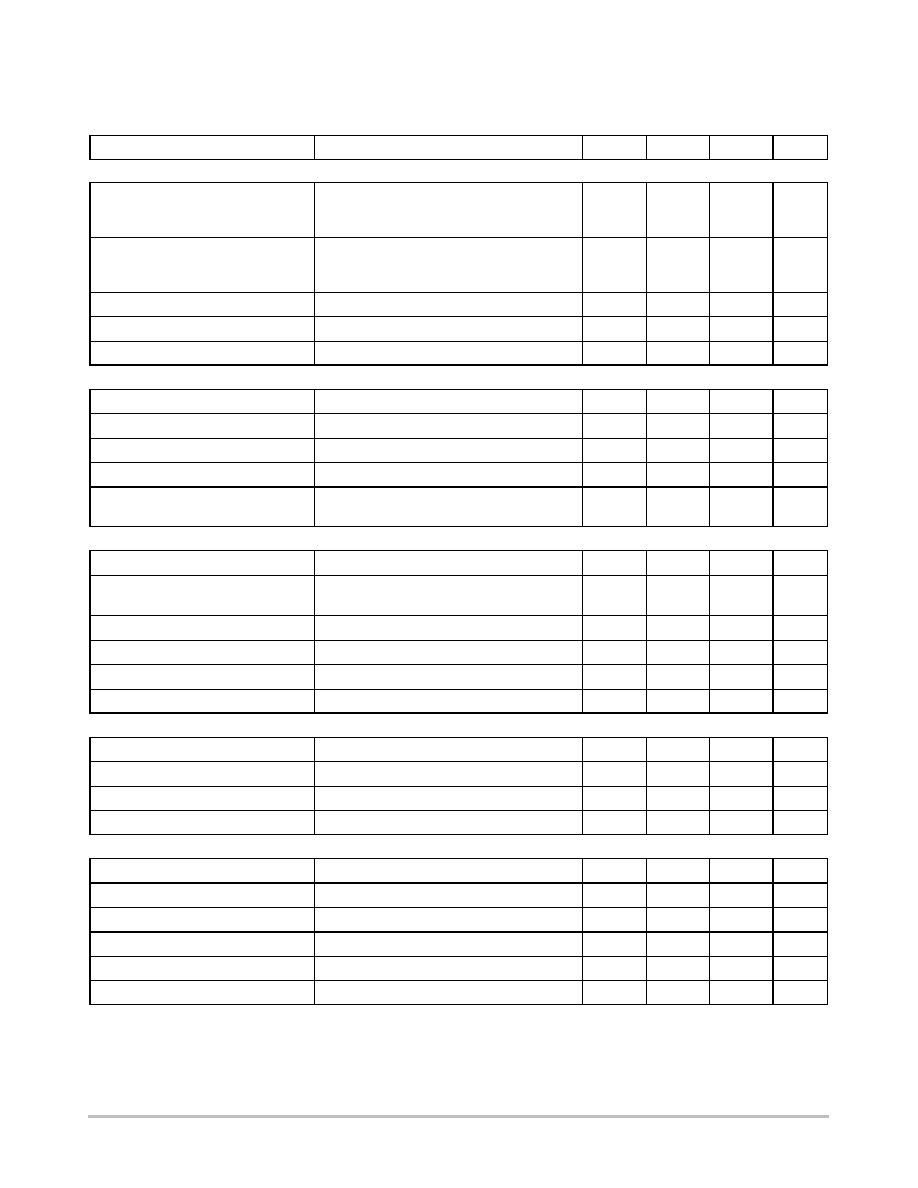
ELECTRICAL CHARACTERISTICS
(≠40
∞
C < T
A
< 85
∞
C (CS5212E); 0
∞
C < T
A
< 70
∞
C (CS5212G); ≠40
∞
C < T
J
< 125
∞
C;
3.1
V < V
CC
< 3.5
V; 3.1 V < V
C
< 7.0 V; 4.5 V < BST < 20 V; C
GATE(H)
=
C
GATE(L)
= 3.3
nF; R
OSC
= 51 k; C
COMP
= 0.1
µ
F, unless other-
wise specified.)
Characteristic
Test Conditions
Min
Typ
Max
Unit
Error Amplifier
V
FB
Bias Current
V
FB
= 0 V
≠
0.1
1.0
µ
A
COMP Source Current
V
FB
= 0.8 V
15
30
60
µ
A
COMP SINK Current
V
FB
= 1.2 V
15
30
60
µ
A
Open Loop Gain
≠
≠
98
≠
dB
Unity Gain Bandwidth
C = 0.1
µ
F
≠
50
≠
kHz
PSRR @ 1.0 kHz
≠
≠
70
≠
dB
Output Transconductance
≠
≠
32
≠
mmho
Output Impedance
≠
≠
2.5
≠
M
Reference Voltage
≠0.1 V < SGND < 0.1 V,
COMP = V
FB
, Measure V
FB
to SGND
0.977
0.992
1.007
V
COMP Max Voltage
V
FB
= 0.8 V
2.5
3.0
≠
V
COMP Min Voltage
V
FB
= 1.2 V
≠
0.1
0.2
V
GATE(H) and GATE(L)
High Voltage (AC)
GATE(L)
GATE(H)
0.5 nF < C
GATE(H)
= C
GATE(L)
< 10 nF. Note 2.
V
C
≠ 0.5
BST ≠ 0.5
≠
≠
≠
≠
V
V
Low Voltage (AC)
GATE(L) or GATE(H)
0.5 nF < C
GATE(H)
; C
GATE(L)
< 10 nF. Note 2.
≠
≠
0.5
V
2. GBD.
CS5212
http://onsemi.com
4
ELECTRICAL CHARACTERISTICS (continued)
(≠40
∞
C < T
A
< 85
∞
C (CS5212E); 0
∞
C < T
A
< 70
∞
C (CS5212G); ≠40
∞
C < T
J
< 125
∞
C;
3.1
V < V
CC
< 3.5
V; 3.1 V < V
C
< 7.0 V; 4.5 V < BST < 20 V; C
GATE(H)
=
C
GATE(L)
= 3.3
nF; R
OSC
= 51 k; C
COMP
= 0.1
µ
F, unless other-
wise specified.)
Characteristic
Unit
Max
Typ
Min
Test Conditions
GATE(H) and GATE(L)
Rise Time
V
C
= BST = 7.0 V, Measure:
0.7 V < GATE(L) < 6.3 V,
0.7 V < GATE(H) < 6.3 V
≠
40
80
ns
Fall Time
V
C
= BST = 7.0 V, Measure:
0.7 V < GATE(L) < 6.3 V,
0.7 V < GATE(H) < 6.3 V
≠
40
80
ns
GATE(H) to GATE(L) Delay
GATE(H) < 2.0 V, GATE(L) > 2.0 V
40
70
110
ns
GATE(L) to GATE(H) Delay
GATE(L) < 2.0 V, GATE(H) > 2.0 V
40
70
110
ns
GATE(H)/(L) Pull≠Down
Resistance to PGND
20
50
115
K
Overcurrent Protection
OVC Comparator Offset Voltage
0 V < IS+ < V
CC
, 0 V < IS≠ < V
CC
54
60
66
mV
IS+ Bias Current
0 V < IS+ < V
CC
≠1.0
0.1
1.0
µ
A
IS≠ Bias Current
0 V < IS≠ < V
CC
≠1.0
0.1
1.0
µ
A
COMP Discharge Threshold
≠
0.20
0.25
0.30
V
COMP Discharge Current in OVC
Fault Mode
COMP = 1.0 V
2.0
5.0
8.0
µ
A
PWM Comparator
Transient Response
COMP = 0 ≠ 1.5 V, V
FFB
, 20 mV overdrive
≠
100
200
ns
PWM Comparator Offset
V
FB
= V
FFB
= 0 V; Increase COMP until
GATE(H) starts switching
0.35
0.40
0.45
V
Artificial Ramp
Duty Cycle = 90%
40
70
100
mV
V
FFB
Bias Current
V
FFB
= 0 V
≠
0.1
1.0
µ
A
V
FFB
Input Range
Note 3.
≠
≠
1.1
V
Minimum Pulse Width
≠
≠
≠
200
ns
Oscillator
Switching Frequency
R
OSC
= 18 k
600
750
900
kHz
Switching Frequency
R
OSC
= 51 k
240
300
360
kHz
Switching Frequency
R
OSC
= 115 k
120
150
180
kHz
R
OSC
Voltage
≠
1.21
1.25
1.29
V
General Electrical Specifications
V
CC
Supply Current
COMP = 0 V (no switching)
≠
5.0
8.0
mA
BST/V
C
Supply Current
COMP = 0 V (no switching)
≠
2.0
3.0
mA
Start Threshold
GATE(H) Switching, COMP Charging
2.7
2.8
2.9
V
Stop Threshold
GATE(H) Not Switching, COMP Not Charging
2.6
2.7
2.8
V
Hysteresis
Start≠Stop
75
100
125
mV
Sense Ground Current
Note 4.
≠
0.15
1.00
mA
3. GBD.
4. Recommended maximum operating voltage between the three grounds is 200 mV.
CS5212
http://onsemi.com
5
PACKAGE PIN DESCRIPTION
PIN NO.
PIN SYMBOL
FUNCTION
1
GATE(H)
High Side Switch FET driver pin. Capable of delivering peak currents of 1.0 A.
2
BST
Power supply input for the high side driver.
3
LGND
Reference ground. All control circuits are referenced to this pin. IC substrate connection.
4
V
FFB
Input for the PWM comparator.
5
V
FB
Error amplifier input.
6
COMP
Error Amp output. PWM Comparator reference input. A capacitor to LGND provides error amp
compensation.
7
SGND
Internal reference is connected to this ground. Connect directly at the load for ground remote
sensing.
8
R
OSC
A resistor from this pin to SGND sets switching frequency.
9
V
CC
Input Power Supply Pin. It supplies power to control circuitry. A 0.1
µ
F Decoupling cap is
recommended.
10
IS≠
Negative input for overcurrent comparator.
11
IS+
Positive input for overcurrent comparator.
12
V
C
Power supply input for the low side driver.
13
GATE(L)
Low Side Synchronous FET driver pin. Capable of delivering peak currents of 1.0 A.
14
PGND
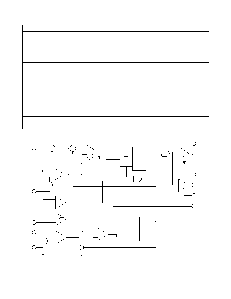
High Current ground for the GATE(H) and GATE(L) pins.
+
UVLO
Comparator
5.0
µ
A
GATE(L)
GATE(H)
-
+
-
+
-
+
-
+
-
+
-
+
-
-
+
-
+
PGND
R
OSC
V
C
BST
R
S
Q
Q
S
R
Q
Q
Fault
Fault
PWM FF
COMP Discharge COMP
0.25 V
PWM Comparator
ART Ramp
OSC
R
OSC
0.5 V
Error Amp
1.0 V
100 % DC
Comparator
V
START
OC
Comparator
60 mV
0.8 V
UVLO
LGND
V
CC
IS≠
IS+
SGND
V
FB
COMP
V
FFB
Figure 2. Block Diagram
Reset Dominant
Set Dominant
CS5212
http://onsemi.com
6
THEORY OF OPERATION
The CS5212 is a synchronous, programmable
fixed≠frequency, low≠voltage buck controller using the V
2
control method. It also provides overcurrent protection,
undervoltage lockout, soft start and built≠in adaptive
non≠overlap.
V
2
Control Method
The V
2
method of control uses a ramp signal generated by
the ESR of the output capacitors. This ramp is proportional
to the AC current through the main inductor and is offset by
the value of the DC output voltage. This control scheme
inherently compensates for variations in either line or load
conditions, since the ramp signal is generated from the
output voltage itself. This control scheme differs from
traditional techniques such as voltage mode, which
generates an artificial ramp, and current mode, which
generates a ramp from inductor current.
-
+
-
+
Ramp Signal
Error Signal
Error Amplifier
COMP
GATE(L)
GATE(H)
Output
Voltage
Feedback
PWM Comparator
Figure 3. V
2
Control Block Diagram
Reference
Voltage
As illustrated in Figure 3, the output voltage is used to
generate both the error signal and the ramp signal. Since the
ramp signal is simply the output voltage, it is affected by any
change in the output regardless of the origin of the change.
The ramp signal also contains the DC portion of the output
voltage, which allows the control circuit to drive the main
switch to 0% or 100% duty cycle as required.
A change in line voltage changes the current ramp in the
inductor, affecting the ramp signal, which causes the V
2
control scheme to compensate the duty cycle. Since the
change in the inductor current modifies the ramp signal, as
in current mode control, the V
2
control scheme has the same
advantages in line transient response.
A change in load current will have an effect on the output
voltage, altering the ramp signal. A load step immediately
changes the state of the comparator output, which controls
the main switch. Load transient response is determined only
by the comparator response time and the transition speed of
the main switch. The reaction time to an output load step has
no relation to the crossover frequency of the error signal
loop, compared to traditional control methods.
The error signal loop can have a low crossover frequency,
since transient response is handled by the ramp signal loop.
The main purpose of this "slow" feedback loop is to provide
DC accuracy. Noise immunity is significantly improved,
because the error amplifier bandwidth can be rolled off at a
low frequency. Enhanced noise immunity improves remote
sensing of the output voltage, since the noise associated with
long feedback traces can be effectively filtered.
Line and load regulations are drastically improved
because there are two independent voltage loops. A voltage
mode controller relies on a change in the error signal to
compensate for a deviation in either line or load voltage.
This change in the error signal causes the output voltage to
change corresponding to the gain of the error amplifier,
which is normally specified as line and load regulation. A
current mode controller maintains fixed error signal under
deviation in the line voltage, since the slope of the ramp
signal changes, but still relies on a change in the error signal
for a deviation in load. The V
2
method of control maintains
a fixed error signal for both line and load variations, since
both line and load affect the ramp signal.
Constant Frequency Operation
The CS5212 uses a constant frequency, trailing edge
modulation architecture for generating PWM signal. During
normal operation, the oscillator generates a narrow pulse at
the beginning of each switching cycle to turn on the main
switch. The main switch will be turned off when the ramp
signal intersects with the output of the error amplifier
(COMP pin voltage). Therefore, the switch duty cycle can
be modified to regulate the output voltage to the desired
value as line and load conditions change.
The major advantage of constant frequency operation is
that the component selections, especially the magnetic
component design, become very easy. The oscillator
frequency of CS5212 is programmable from 150 kHz to
750 kHz using an external resistor connected from the R
OSC
pin to ground.
Startup
If there are no fault conditions and the fault latch is reset,
the error amplifier will start charging the COMP pin
capacitor after the CS5212 is powered up. The output of the
error amplifier (COMP voltage) will ramp up linearly. The
COMP capacitance and the source current of the error
amplifier determine the slew rate of COMP voltage. The
output of the error amplifier is connected internally to the
inverting input of the PWM comparator and it is compared
with the V
FFB
pin voltage plus 0.5 V offset at the
non≠inverting input of the PWM comparator. Since V
FFB
voltage is zero before the startup, the PWM comparator
output will stay high until the COMP pin voltage hits 0.5 V.
There is no switching action while the PWM comparator
output is high.
After the COMP voltage exceeds the 0.5 V offset, the
output of PWM comparator toggles and releases the PWM
latch. The narrow pulse generated by the oscillator at the
CS5212
http://onsemi.com
7
beginning of the next oscillator cycle will set the latch so that
the main switch can be turned on and the regulator output
voltage ramps up. When the output voltage achieves a level
set by the COMP voltage, the main switch will be turned off.
The V
2
control loop will adjust the main switch duty cycle
as required to ensure the regulator output voltage tracks the
COMP voltage. Since the COMP voltage increases
gradually,
the soft start can be achieved. The start≠up period
ends when the output voltage reaches the level set by the
external resistor divider.
Output Enable
Since there can be no switching until the COMP pin
exceeds the 0.5 V offset built into the PWM comparator, the
COMP pin can also be used for an enable function. Hold the
COMP pin below 0.4 V with an open collector circuit to
disable the output. When the COMP pin is released to enable
startup, the user must ensure there is no leakage current from
the enable circuit into COMP. During normal operation the
COMP output is driven with only 5.0
µ
A to 30
µ
A internally.
Hiccup Mode Overcurrent Protection
Under normal load conditions, the voltage across the IS+
and IS≠ pins is less than the 60 mV overcurrent threshold. If
the threshold is exceeded, the overcurrent fault latch is set,
the high side gate driver is forced low, and the COMP pin is
discharged with 5.0
µ
A. There is no switching until the
COMP voltage drops below a 0.25 V threshold. Then, the
fault latch is cleared and a soft start is initiated. The low
effective duty cycle during hiccup overcurrent greatly
reduces component stress for an extended fault.
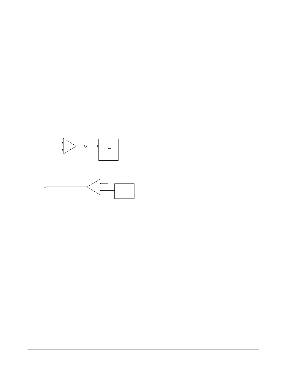
Inductor Current Sensing
Besides using a current sense resistor to sense inductor
current, CS5212 provides the users with the possibility of
using loss≠less inductor sensing technique. This sensing
technique utilizes the Equivalent Series Resistance (ESR) of
the inductor to sense the current. The output current is
sensed through an RC network in parallel with the inductor
as shown in Figure 4. The voltage across the small capacitor
is then fed to the OC comparator.
R
RL
C
Q1
IS≠
IS+
C
O
V
IN
Figure 4. Inductor Current Sensing
Q2
L
If the values of R and C are chosen such that:
L
RL
+
RC
Then the voltage across the capacitor C will be:
VC
+
RLIL
Therefore, if the time constant of the RC network is equal
to that of the inductor, the voltage across the capacitor is
proportional to the inductor current by a factor of the
inductor ESR. In practice, the user should ensure that under
all component tolerances, the RC time constant is larger than
the L/R time constant. This will keep the high frequency
gain for V
C
(s)/I
L
(s) less than the low frequency gain, and
avoid unnecessary OCP tripping during short duration
overcurrent situations.
Compared with conventional resistor sensing, the
inductor
ESR current sensing technique is lossless, but is not
as accurate due to variation in the ESR from inductor to
inductor and over temperature. For typical inductor ESR, the
0.39%/
∞
C positive temperature coefficient will reduce the
current limit at high temperature, and will help prevent
thermal runaway, but will force an increased design target at
room temperature. This technique can be more accurate than
using a PCB trace, since PCB copper thickness can vary
10≠20%, compared to 1% variation in wire diameter
thickness typical of inductors.
Remote Voltage Sensing
The CS5212 has the capability to sense the voltage when
the load is located far away from the regulator. The SGND
pin is dedicated to the differential remote sensing. The
negative remote sense line is connected to SGND pin
directly, while the positive remote sense line is usually
connected to the top of the feedback voltage divider. To
prevent over≠voltage condition caused by open remote
sense lines, the divider should also be locally connected to
the output of the regulator through a low value resistor. That
resistor is used to compensate for the voltage drop across the
output power cables.

CS5212
http://onsemi.com
8
APPLICATIONS INFORMATION
APPLICATIONS AND COMPONENT SELECTION
Inductor Component Selection
The output inductor may be the most critical component
in the converter because it will directly effect the choice of
other components and dictate both the steady≠state and
transient performance of the converter. When selecting an
inductor the designer must consider factors such as DC
current, peak current, output voltage ripple, core material,
magnetic saturation, temperature, physical size, and cost
(usually the primary concern).
In general, the output inductance value should be as low
and physically small as possible to provide the best transient
response and minimum cost. If a large inductance value is
used, the converter will not respond quickly to rapid changes
in the load current. On the other hand, too low an inductance
value will result in very large ripple currents in the power
components (MOSFETs, capacitors, etc) resulting in
increased dissipation and lower converter efficiency. Also,
increased ripple currents will force the designer to use
higher rated MOSFETs, oversize the thermal solution, and
use more, higher rated input and output capacitors ≠ the
converter cost will be adversely effected.
One method of calculating an output inductor value is to
size the inductor to produce a specified maximum ripple
current in the inductor. Lower ripple currents will result in
less core and MOSFET losses and higher converter
efficiency. The following equation may be used to calculate
the minimum inductor value to produce a given maximum
ripple current (
I
O,MAX
). The inductor value calculated by
this equation is a minimum because values less than this will
produce more ripple current than desired. Conversely,
higher inductor values will result in less than the maximum
ripple current.
LoMIN
+
(Vin
*
Vout)
@
Vout (
a @
IO,MAX
@
Vin
@
fSW)
is the ripple current as a percentage of the maximum
output current (
= 0.15 for
±
15%,
= 0.25 for
±
25%, etc)
and f
sw
is the switching frequency. If the minimum inductor
value is used, the inductor current will swing
±
/2% about
Iout. Therefore, the inductor must be designed or selected
such that it will not saturate with a peak current of (1 +
/2)
I
O,MAX
.
Power dissipation in the inductor can now be calculated
from the RMS current level. The RMS of the AC component
of the inductor is given by the following relationship:
IAC
+
IPP
12
where I
PP
=
I
O,MAX
.
The total I
RMS
of the current will be calculated from:
IRMS
+
IOUT2
)
IAC2
The power dissipation for the inductor can be determined
from:
P
+
IRMS2
RL
Input Capacitor Selection and Considerations
The input capacitor is used to reduce the current surges
caused by conduction of current of the top pass transistor
charging the PWM inductor.
The input current is pulsing at the switching frequency
going from 0 to peak current in the inductor. The duty factor
will be a function of the ratio of the input to output voltage
and of the efficiency.
DF
+
VO
VI
1
Eff
The RMS value of the ripple into the input capacitors can
now be calculated:
IIN(RMS)
+
IOUT DF
*
DF2
The input RMS is maximum at 50% DF, so selection of the
possible duty factor closest to 50% will give the worst case
dissipation in the capacitors. The power dissipation of the
input capacitors can be calculated by multiplying the square
of the RMS current by the ESR of the capacitor.
Output Capacitor
The output capacitor filters output inductor ripple current
and provides low impedance for load current changes. The
effect of the capacitance for handling the power supply
induced ripple will be discussed here. Effects of load
transient behavior can be considered separately.
The principle consideration for the output capacitor is the
ripple current induced by the switches through the inductor.
This ripple current was calculated as I
AC
in the above
discussion of the inductor. This ripple component will
induce heating in the capacitor by a factor of the RMS
current squared multiplied by the ESR of the output
capacitor section. It will also create output ripple voltage.
The ripple voltage will be a vector summation of the ripple
current times the ESR of the capacitor, plus the ripple current
integrating in the capacitor, and the rate of change in current
times the total series inductance of the capacitor and
connections.
The inductor ripple current acting against the ESR of the
output capacitor is the major contributor to the output ripple
voltage. This fact can be used as a criterion to select the
output capacitor.
VPP
+
IPP
CESR
The power dissipation in the output capacitor can be
calculated from:
P
+
IAC2
CESR
where:
I
AC
= AC RMS of the inductor
C
ESR
= Effective series resistance of the output capacitor
network.
CS5212
http://onsemi.com
9
MOSFET & Heatsink Selection
Power dissipation, package size, and thermal solution
drive MOSFET selection. To adequately size the heat sink,
the design must first predict the MOSFET power dissipation.
Once the dissipation is known, the heat sink thermal
impedance can be calculated to prevent the specified
maximum case or junction temperatures from being exceeded
at the highest ambient temperature. Power dissipation has two
primary contributors: conduction losses and switching losses.
The control or upper MOSFET will display both switching
and conduction losses. The synchronous or lower MOSFET
will exhibit only conduction losses because it switches into
nearly zero voltage. However, the body diode in the
synchronous MOSFET will suffer diode losses during the
non≠overlap time of the gate drivers.
For the upper or control MOSFET, the power dissipation
can be approximated from:
PD,CONTROL
+
(IRMS,CNTL2
@
RDS(on))
)
(ILo,MAX
@
Qswitch Ig
@
VIN
@
fSW)
)
(Qoss 2
@
VIN
@
fSW)
)
(VIN
@
QRR
@
fSW)
The first term represents the conduction or IR losses when
the MOSFET is ON while the second term represents the
switching losses. The third term is the losses associated with
the control and synchronous MOSFET output charge when
the control MOSFET turns ON. The output losses are caused
by both the control and synchronous MOSFET but are
dissipated only in the control FET. The fourth term is the loss
due to the reverse recovery time of the body diode in the
synchronous MOSFET. The first two terms are usually
adequate to predict the majority of the losses.
Where I
RMS,CNTL
is the RMS value of the trapezoidal
current in the control MOSFET:
IRMS,CNTL
+
D
@
[(ILo,MAX2
)
ILo,MAX
@
ILo,MIN
)
ILo,MIN2) 3]1 2
I
Lo,MAX
is the maximum output inductor current:
ILo,MAX
+
IO,MAX 2
) D
ILo 2
I
Lo,MIN
is the minimum output inductor current:
ILo,MIN
+
IO,MAX 2
* D
ILo 2
I
O,MAX
is the maximum converter output current.
D is the duty cycle of the converter:
D
+
VOUT VIN
I
Lo
is the peak≠to≠peak ripple current in the output
inductor of value Lo:
D
ILo
+
(VIN
*
VOUT)
@
D (Lo
@
fSW)
R
DS(on)
is the ON resistance of the MOSFET at the
applied gate drive voltage.
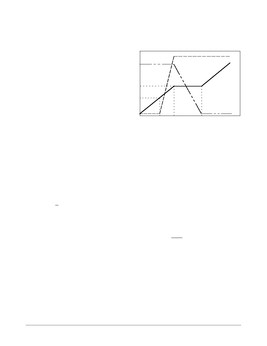
Q
switch
is the post gate threshold portion of the
gate≠to≠source charge plus the gate≠to≠drain charge. This
may be specified in the data sheet or approximated from the
gate≠charge curve as shown in the Figure 5.
Qswitch
+
Qgs2
)
Qgd
I
D
V
GATE
V
DRAIN
Q
GD
Q
GS2
Q
GS1
V
GS_TH
Figure 5. MOSFET Switching Characteristics
I
g
is the output current from the gate driver IC.
V
IN
is the input voltage to the converter.
f
sw
is the switching frequency of the converter.
Q
G
is the MOSFET total gate charge to obtain R
DS(on)
.
Commonly specified in the data sheet.
V
g
is the gate drive voltage.
Q
RR
is the reverse recovery charge of the lower MOSFET.
Q
oss
is the MOSFET output charge specified in the data
sheet.
For the lower or synchronous MOSFET, the power
dissipation can be approximated from:
PD,SYNCH
+
(IRMS,SYNCH2
@
RDS(on))
)
(Vfdiode
@
IO,MAX 2
@
t_nonoverlap
@
fSW)
The first term represents the conduction or IR losses when
the MOSFET is ON and the second term represents the diode
losses that occur during the gate non≠overlap time.
All terms were defined in the previous discussion for the
control MOSFET with the exception of:
IRMS,SYNCH
+
1
*
D
@
[(ILo,MAX2
)
ILo,MAX
@
ILo,MIN
)
ILo,MIN2) 3]1 2
where:
Vf
diode
is the forward voltage of the MOSFET's intrinsic
diode at the converter output current.
t_nonoverlap is the non≠overlap time between the upper
and lower gate drivers to prevent cross conduction. This
time is usually specified in the data sheet for the control
IC.
When the MOSFET power dissipations are known, the
designer can calculate the required thermal impedance to
maintain a specified junction temperature at the worst case
ambient operating temperature
CS5212
http://onsemi.com
10
q
T
t
(TJ
*
TA) PD
where;
T
is the total thermal impedance (
JC
+
SA
).
JC
is the junction≠to≠case thermal impedance of the
MOSFET.
SA
is the sink≠to≠ambient thermal impedance of the
heatsink assuming direct mounting of the MOSFET (no
thermal "pad" is used).
T
J
is the specified maximum allowed junction
temperature.
T
A
is the worst case ambient operating temperature.
For TO≠220 and TO≠263 packages, standard FR≠4
copper clad circuit boards will have approximate thermal
resistances (
SA
) as shown below:
Pad Size
(in
2
/mm
2
)
Single≠Sided
1 oz. Copper
0.5/323
60≠65
∞
C/W
0.75/484
55≠60
∞
C/W
1.0/645
50≠55
∞
C/W
1.5/968
45≠50
∞
C/W
2.0/1290
38≠42
∞
C/W
2.5/1612
33≠37
∞
C/W
As with any power design, proper laboratory testing
should be performed to insure the design will dissipate the
required power under worst case operating conditions.
Variables considered during testing should include
maximum ambient temperature, minimum airflow,
maximum
input voltage, maximum loading, and component
variations (i.e. worst case MOSFET R
DS(on)
). Also, the
inductors and capacitors share the MOSFET's heatsinks and
will add heat and raise the temperature of the circuit board
and MOSFET. For any new design, its advisable to have as
much heatsink area as possible ≠ all too often new designs
are found to be too hot and require re≠design to add
heatsinking.
Compensation Capacitor Selection
The nominal output current capability of the error amp is
30
µ
A. This current charging the capacitor on the COMP pin
is used as soft start for the converter. The COMP pin is going
to ramp up to a voltage level that is within 70 mV of what
V
FFB
is going to be when in regulation. This is the voltage
that will determine the soft start. Therefore, the COMP
capacitor can be established by the following relationship:
C
+
30
m
A
soft start
VFFB(REG)
where:
soft start = output ramp≠up time
V
FFB(REG)
= V
FFB
voltage when in regulation
30
µ
A = COMP output current, typ.
The COMP output current range is given in the data sheet
and will affect the ramp≠up time. The value of the capacitor
on the COMP pin will have an effect on the loop response
and the transient response of the converter. Transient
response can be enhanced by the addition of a parallel
combination of a resistor and capacitor between the COMP
pin and the comp capacitor.
R
OSC
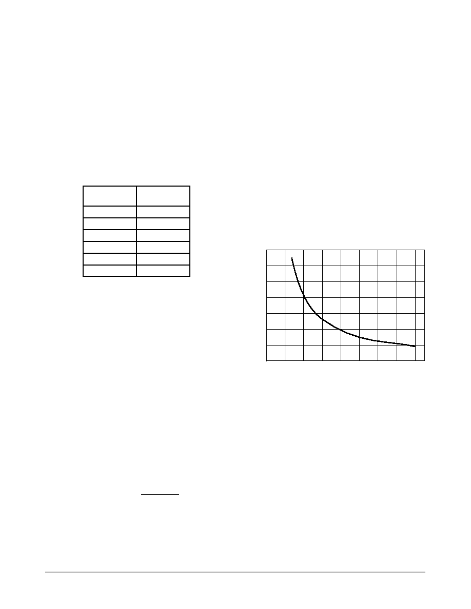
Selection
The switching frequency is programmed by selecting the
resistor connected between the R
OSC
pin and SGND (pin 7).
The grounded side of this resistor should be directly
connected to the SGND pin, without any other currents
flowing between the bottom of the resistor and the pin. Also,
avoid running any noisy signals under the resistor, since
injected noise could cause frequency jitter. The graph in
Figure NO TAG shows the required resistance to program
the frequency. Below 500 kHz, the following formula is
accurate:
R
+
17544 fSW
*
4 k
W
where f
SW
is the switching frequency in kHz.
Figure 6. Frequency vs. R
OSC
0
Resistance
(k
)
0
Frequency (kHz)
20
40
60
80
100
120
140
100
200
300
400
500
600
700
800
Differential Remote Sense Operation
The ability to implement fully differential remote sense is
provided by the CS5212. The positive remote sense is
implemented by bringing the output remote sense
connection to the positive load connection. A low value
resistor is connected from Vout to the feedback point at the
regulator to provide feedback in the instance when the
remote sense point is not connected.
The negative remote sense connection is provided by
connecting the SGND of the CS5212 to the negative of the
load return. Again, a low value resistor should be connected
between SGND and LGND at the regulator to provide
feedback in the instance when the remote sense point is not
connected. The maximum voltage differential between the
three grounds for this part is 200 mV.
CS5212
http://onsemi.com
11
Feedback Divider Selection
The feedback voltage measured at V
FB
during normal
regulation will be 1.0 V. This voltage is compared to an
internal 1.0 V reference and is used to regulate the output
voltage. The bias current into the error amplifier is 1.0
µ
A
max, so select the resistor values so that this current does not
add an excessive offset voltage.
V
FFB
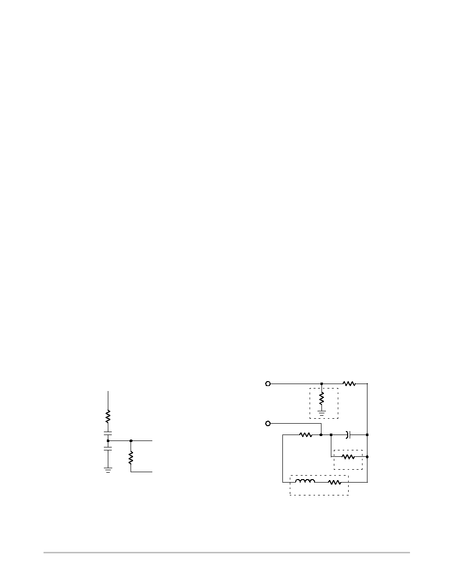
Feedback Selection
To take full advantage of the V
2
control scheme, a small
amount of output ripple must be fed back to the V
FFB
pin,
typically 50 mV. For most application, this requirement is
simple to achieve and the V
FFB
can be connected directly to
the V
FB
pin. There are some application that have to meet
stringent load transient requirements. One of the key factor
in achieving tight dynamic voltage regulation is low ESR.
Low ESR at the regulator output results in low output
voltage ripple. This situation could result in increase noise
sensitivity and a potential for loop instability. In applications
where the output ripple is not sufficient, the performance of
the CS5212 can be improved by adding a fixed amount
external ramp compensation to the V
FFB
pin. Refer to Figure
7, the amount of ramp at the V
FFB
pin depends on the switch
node Voltage, Feedback Voltage, R1 and C2.
Vramp
+
(Vsw
*
VFB)
ton (R1
C2)
where:
Vramp = amount of ramp needed;
Vsw = switch note voltage;
V
FB
= voltage feedback, 1 V;
ton = switch on≠time.
To minimize the lost in efficiency R1 resistance should be
large, typically 100 k or larger. With R1 chosen, C2 can be
determined by the following;
C2
+
(Vsw
*
VFB)
ton (R1
Vramp)
C1 is used as a bypass capacitor and its value should be
equal to or greater than C2.
Figure 7. Small RC Filter Providing the Proper Voltage
Ramp at the Beginning of Each On≠Time Cycle
Vsw
R2
1.0 k
V
FFB
V
FB
R1
C1
C2
Maximum Frequency Operation
The minimum pulse width may limit the maximum
operating frequency. The duty factor, given by the
output/input voltage ratio, multiplied by the period
determines the pulse width during normal operation. This
pulse width must be greater than 200 ns, or duty cycle jitter
could become excessive. For low pulse widths below 300 ns,
external slope compensation should be added to the V
FFB
pin to increase the PWM ramp signal and improve stability.
50 mV of added ramp at the V
FFB
pin is typically enough.
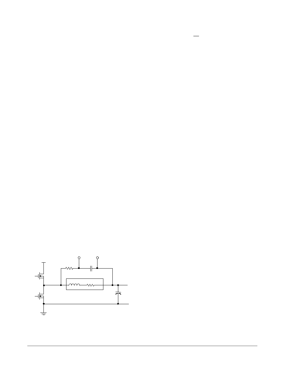
Current Sense Component Selection
The current limit threshold is set by sensing a 60 mV
voltage differential between the IS+ and IS≠ pins. Referring
to Figure 8, the time constant of the R2,C1 filter should be
set larger than the L/R1 time constant under worst case
tolerances, to prevent overshoot in the sensed voltage and
tripping the current limit too low. Resistor R3 of value equal
to R2 is added for bias current cancellation. R2 and R3
should not be made too large, to reduce errors from bias
current offsets. For typical L/R time constants, a 0.1
µ
F
capacitor for C1 will allow R2 to be between 1.0 k and 10 k
.
The current limit without R4 and R5, which are optional,
is given by 60 mV/R1, where R1 is the internal resistance of
the inductor, obtained from the manufacturer. The addition
of R5 can be used to decrease the current limit to a value
given by:
ILIM
+
(60 mV
*
(VOUT
R3 (R3
)
R5)) R1
where V
OUT
is the output voltage.
Similiarly, omitting R5 and adding R4 will increase the
current limit to a value given by:
ILIM
+
60 mV R1
(1
)
R2 R4)
Essentially, R4 or R5 are used to increase or decrease the
inductor voltage drop which corresponds to 60 mV at the IS+
and IS≠ pins.
Figure 8. Current Limit
R5
R3
IS≠
IS+
R2
60 mV Trip
R4
C1
R1
L1
L
V
OUT
Switching
Node

CS5212
http://onsemi.com
12
Boost Component Selection for Upper and Lower
FET Gate Drive
The boost (BST) pin provides for application of a higher
voltage to drive the upper FET. This voltage may be
provided by a fixed higher voltage or it may be generated
with a boost capacitor and charging diodes, as shown in
Figure 1. The voltage in the boost configuration would be
the summation of the voltage from the charging diodes and
the output voltage swing. Care must be taken to keep the
peak voltage with respect to ground less than 20 V peak. The
capacitor value should be ten times larger than the
capacitance of the top FET. The boost circuit requires a
modification to achieve startup. See Rpull≠up Selection for
boost circuit startup.
Rpull≠up Value Selection for Boost Circuit Startup
The CS5212 application circuit incorporates a pull≠up
resistor, R7, into the boost circuitry. This resistor is essential
to achieving startup of the boost circuit. At startup, the
GATE(H) output may be limited to 0.8 V, due to internal Vbe
drops. Until the boost circuitry charges up, the GATE(H)
output cannot provide sufficient Vgs to turn on the
MOSFET. A resistor from GATE(H) to BST allows
bypassing of the GATE(H) driver until the boost circuitry is
charged. The time constant, set by the pull≠up resistor and
the Cin of the top MOSFET, must be fast enough to turn on
the MOSFET during the switching period. The following
equation is used to determine Rpull≠up:
Rpull≠up
t
1
(Cin
fSW)
where f
SW
is the switching frequency.
Choosing components according to this equation will
insure that approximately 63% of the boost voltage will be
applied to GATE(H) within one switching period. To start
charge pumping, the control MOSFET must pull up the
switching node above 0.6 V, two Schottky drops, which will
allow V
C
voltage to increase. Therefore, the voltage applied
by GATE(H) must be 0.6 V greater than Vth of the top FET.
Both high≠ and low≠side switches must be sublogic level
MOSFETs with R
DS(on)
specified at 2.5 Vgs in order to
ensure proper up.
CS5212
http://onsemi.com
13
ORDERING INFORMATION
Device
Operating Temperature Range
Package
Shipping
CS5212ED14
40
∞
C < T < 85
∞
C
SO≠14
55 Units/Rail
CS5212EDR14
≠40
∞
C < T
A
< 85
∞
C
SO≠14
2500 Tape & Reel
CS5212GD14
0
∞
C < T < 70
∞
C
SO≠14
55 Units/Rail
CS5212GDR14
0
∞
C < T
A
< 70
∞
C
SO≠14
2500 Tape & Reel
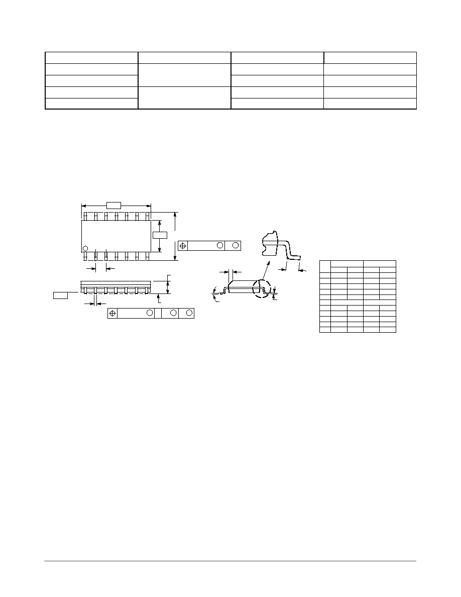
PACKAGE DIMENSIONS
NOTES:
1. DIMENSIONING AND TOLERANCING PER ANSI
Y14.5M, 1982.
2. CONTROLLING DIMENSION: MILLIMETER.
3. DIMENSIONS A AND B DO NOT INCLUDE
MOLD PROTRUSION.
4. MAXIMUM MOLD PROTRUSION 0.15 (0.006)
PER SIDE.
5. DIMENSION D DOES NOT INCLUDE DAMBAR
PROTRUSION. ALLOWABLE DAMBAR
PROTRUSION SHALL BE 0.127 (0.005) TOTAL
IN EXCESS OF THE D DIMENSION AT
MAXIMUM MATERIAL CONDITION.
≠A≠
≠B≠
G
P
7 PL
14
8
7
1
M
0.25 (0.010)
B
M
S
B
M
0.25 (0.010)
A
S
T
≠T≠
F
R
X 45
SEATING
PLANE
D
14 PL
K
C
J
M
_
DIM
MIN
MAX
MIN
MAX
INCHES
MILLIMETERS
A
8.55
8.75
0.337
0.344
B
3.80
4.00
0.150
0.157
C
1.35
1.75
0.054
0.068
D
0.35
0.49
0.014
0.019
F
0.40
1.25
0.016
0.049
G
1.27 BSC
0.050 BSC
J
0.19
0.25
0.008
0.009
K
0.10
0.25
0.004
0.009
M
0
7
0
7
P
5.80
6.20
0.228
0.244
R
0.25
0.50
0.010
0.019
_
_
_
_
SO≠14
D SUFFIX
CASE 751A≠03
ISSUE F

CS5212
http://onsemi.com
14
Notes

CS5212
http://onsemi.com
15
Notes

CS5212
http://onsemi.com
16
ON Semiconductor and are registered trademarks of Semiconductor Components Industries, LLC (SCILLC). SCILLC reserves the right to make
changes without further notice to any products herein. SCILLC makes no warranty, representation or guarantee regarding the suitability of its products for any
particular purpose, nor does SCILLC assume any liability arising out of the application or use of any product or circuit, and specifically disclaims any and all
liability, including without limitation special, consequential or incidental damages. "Typical" parameters which may be provided in SCILLC data sheets and/or
specifications can and do vary in different applications and actual performance may vary over time. All operating parameters, including "Typicals" must be
validated for each customer application by customer's technical experts. SCILLC does not convey any license under its patent rights nor the rights of others.
SCILLC products are not designed, intended, or authorized for use as components in systems intended for surgical implant into the body, or other applications
intended to support or sustain life, or for any other application in which the failure of the SCILLC product could create a situation where personal injury or death
may occur. Should Buyer purchase or use SCILLC products for any such unintended or unauthorized application, Buyer shall indemnify and hold SCILLC
and its officers, employees, subsidiaries, affiliates, and distributors harmless against all claims, costs, damages, and expenses, and reasonable attorney fees
arising out of, directly or indirectly, any claim of personal injury or death associated with such unintended or unauthorized use, even if such claim alleges that
SCILLC was negligent regarding the design or manufacture of the part. SCILLC is an Equal Opportunity/Affirmative Action Employer.
PUBLICATION ORDERING INFORMATION
JAPAN: ON Semiconductor, Japan Customer Focus Center
4≠32≠1 Nishi≠Gotanda, Shinagawa≠ku, Tokyo, Japan 141≠0031
Phone: 81≠3≠5740≠2700
Email: r14525@onsemi.com
ON Semiconductor Website: http://onsemi.com
For additional information, please contact your local
Sales Representative.
CS5212/D
V
2
is a trademark of Switch Power, Inc.
Literature Fulfillment:
Literature Distribution Center for ON Semiconductor
P.O. Box 5163, Denver, Colorado 80217 USA
Phone: 303≠675≠2175 or 800≠344≠3860 Toll Free USA/Canada
Fax: 303≠675≠2176 or 800≠344≠3867 Toll Free USA/Canada
Email: ONlit@hibbertco.com
N. American Technical Support: 800≠282≠9855 Toll Free USA/Canada