 | –≠–ª–µ–∫—Ç—Ä–æ–Ω–Ω—ã–π –∫–æ–º–ø–æ–Ω–µ–Ω—Ç: CS5323D | –°–∫–∞—á–∞—Ç—å:  PDF PDF  ZIP ZIP |

©
Semiconductor Components Industries, LLC, 2002
August, 2002 ≠ Rev. 6
1
Publication Order Number:
CS5323/D
CS5323
Three-Phase Buck
Controller with 5-Bit DAC
The CS5323 is a three≠phase step down controller that incorporates
all control functions required to power next generation processors.
Proprietary multi≠phase architecture guarantees balanced load current
distribution and reduces overall solution cost in high current
applications. Enhanced V
2
TM
control architecture provides the fastest
possible transient response, excellent overall regulation, and ease of
use.
The multi≠phase architecture reduces input and output filter ripple,
allowing for a reduction in filter size and inductor values with a
corresponding increase in the output inductor current slew rate.
Features
∑
Enhanced V
2
Control Method
∑
5≠Bit DAC with 1.0% Tolerance
∑
Adjustable Output Voltage Positioning
∑
Programmable Frequency Set by Single Resistor
∑
200
kHz to 800
kHz Operation (Per Phase)
∑
Current Sensed through Sense Resistors, or Buck Inductors
∑
Adjustable Current Sense Threshold
∑
Hiccup Mode Current Limit
∑
Over≠Voltage Protection through Synchronous MOSFET's
∑
Individual Current Limits for Each Phase
∑
On≠Board Current Sense Amplifiers
∑
3.3
V, 1.0
mA Reference Output
∑
5.0
V and/or 12
V Operation
∑
On/Off Control (through COMP Pin)
A
= Assembly Location
WL, L
= Wafer Lot
YY, Y
= Year
WW, W
= Work Week
Device
Package
Shipping
ORDERING INFORMATION
CS5323GDW20
SO≠20L
37 Units/Rail
CS5323GDWR20
SO≠20L
1000 Tape & Reel
COMP
V
FB
V
DRP
CS1
CS2
CS3
CS
REF
V
ID0
V
ID1
V
ID2
V
ID3
V
ID4
I
LIM
REF
R
OSC
V
CC
GATE1
GND
GATE2
GATE3
PIN CONNECTIONS AND
MARKING DIAGRAM
SO≠20L
DW SUFFIX
CASE 751D
CS5323
A
W
L
YWW
1
1
20
http://onsemi.com

CS5323
http://onsemi.com
2
VS
BG
R18
10 k
R19
C17
0.1
µ
F
C4
R6
.01
µ
F
C13
R9
C22
R14
R15
1.0 k
75 k
C20
C16
V
ID4
V
ID3
V
ID1
V
ID0
ENABLE
COMP
V
FB
V
DRP
CS1
CS2
CS3
CS
REF
V
ID0
V
ID2
V
ID3
V
ID4
I
LIM
REF
GATE2
GATE3
Gnd
GATE1
V
CC
R
OSC
V
ID1
CS5323
R17
R16
C21
12 V
IN
5 V
IN
R10
C12
1.0 nF
1.0
µ
F
1.0
µ
F
C19
1.0
µ
F
C27
1.0
µ
F
C26
C23
C24
3
◊
10
µ
F
C4
1.0
µ
F
C5
.01
µ
F
.01
µ
F
.01
µ
F .01
µ
F
30.1 k
30.1 k
30.1 k
2.7 k
1.0 k
0.1
µ
F
C25
V
ID2
R12
D5
Q6
Q5
D3
Q4
Q3
L4
L3
L2
L1
D1
Q2
Gnd
BG
VS
EN
CO
CST
DRN
TG
MTP75N06HD
MTD3302
R13
7.5 k
C11
2.0 nF
EN
CO
CST
DRN
TG
Gnd
C18
1.0
µ
F
Q1
MTD3302
VS
EN
CO
CST
TG
BG
DRN
Gnd
U4
U3
U1
8
◊
4SP560M
850 nH
850 nH
850 nH
BAS40LT1
BAS40LT1
BAS40LT1
+
+
NCP5351
8.0 k
C28
1.0 nF
10 k
U2
R1
10
V
OUT
3
◊
16S0180M
300 nH
MTP75N06HD
MTP75N06HD
MTD3302
Figure 1. Application Diagram, 12 V to 1.7 V Converter
NCP5351
NCP5351

CS5323
http://onsemi.com
3
MAXIMUM RATINGS*
Rating
Value
Unit
Operating Junction Temperature
150
∞
C
Lead Temperature Soldering:
Reflow: (SMD styles only) (Note 1)
230 peak
∞
C
Storage Temperature Range
≠65 to +150
∞
C
ESD Susceptibility (Human Body Model)
2.0
kV
1. 60 second maximum above 183
∞
C.
*The maximum package power dissipation must be observed.
MAXIMUM RATINGS
Pin Number
Pin Symbol
V
MAX
V
MIN
I
SOURCE
I
SINK
1
R
OSC
6.0 V
≠0.3 V
1.0 mA
1.0 mA
2
COMP
6.0 V
≠0.3 V
1.0 mA
1.0 mA
3
V
FB
6.0 V
≠0.3 V
1.0 mA
1.0 mA
4
V
DRP
6.0 V
≠0.3 V
1.0 mA
1.0 mA
5≠7
CS1≠CS3
6.0 V
≠0.3 V
1.0 mA
1.0 mA
8
CS
REF
6.0 V
≠0.3 V
1.0 mA
1.0 mA
9
I
LIM
6.0 V
≠0.3 V
1.0 mA
1.0 mA
10
REF
6.0 V
≠0.3 V
1.0 mA
50 mA
11≠15
VID0≠4
6.0 V
≠0.3 V
1.0 mA
1.0 mA
16
Gnd
0 V
0 V
0.4 A, 1.0
µ
s, 100 mA
DC
N/A
17≠19
GATE 1≠3
16 V
≠0.3 V
0.1 A, 1.0
µ
s, 25 mA DC
0.1 A, 1.0
µ
s, 25 mA DC
20
V
CC
16 V
≠0.3 V
N/A
0.4 A, 1.0
µ
s, 100 mA
DC

CS5323
http://onsemi.com
4
ELECTRICAL CHARACTERISTICS
(0
∞
C < T
A
< 70
∞
C; 0
∞
C < T
J
< 85
∞
C; 4.7
V < V
CC
< 14
V; C
GATE
= 100
pF,
R
R(OSC)
= 53.6
k, C
COMP
= 0.1
µ
F, C
REF
= 0.1
µ
F, DAC Code 10000, C
VCC
= 0.1
µ
F, I
LIM
1.0
V; unless otherwise specified.)
Characteristic
Test Conditions
Min
Typ
Max
Unit
Voltage Identification DAC (0 = Connected to V
SS
; 1 = Open or Pull≠up to 3.3
V)
Accuracy (all codes)
Measure V
FB
= COMP
±
1.0
%
V
ID4
V
ID3
V
ID2
V
ID1
V
ID0
1
1
1
1
1
≠
1.064
1.075
1.086
V
1
1
1
1
0
≠
1.089
1.100
1.111
V
1
1
1
0
1
≠
1.114
1.125
1.136
V
1
1
1
0
0
≠
1.139
1.150
1.162
V
1
1
0
1
1
≠
1.163
1.175
1.187
V
1
1
0
1
0
≠
1.188
1.200
1.212
V
1
1
0
0
1
≠
1.213
1.225
1.237
V
1
1
0
0
0
≠
1.238
1.250
1.263
V
1
0
1
1
1
≠
1.262
1.275
1.288
V
1
0
1
1
0
≠
1.287
1.300
1.313
V
1
0
1
0
1
≠
1.312
1.325
1.338
V
1
0
1
0
0
≠
1.337
1.350
1.364
V
1
0
0
1
1
≠
1.361
1.375
1.389
V
1
0
0
1
0
≠
1.386
1.400
1.414
V
1
0
0
0
1
≠
1.411
1.425
1.439
V
1
0
0
0
0
≠
1.436
1.450
1.465
V
0
1
1
1
1
≠
1.460
1.475
1.490
V
0
1
1
1
0
≠
1.485
1.500
1.515
V
0
1
1
0
1
≠
1.510
1.525
1.540
V
0
1
1
0
0
≠
1.535
1.550
1.566
V
0
1
0
1
1
≠
1.559
1.575
1.591
V
0
1
0
1
0
≠
1.584
1.600
1.616
V
0
1
0
0
1
≠
1.609
1.625
1.641
V
0
1
0
0
0
≠
1.634
1.650
1.667
V
0
0
1
1
1
≠
1.658
1.675
1.692
V
0
0
1
1
0
≠
1.683
1.700
1.717
V
0
0
1
0
1
≠
1.708
1.725
1.742
V
0
0
1
0
0
≠
1.733
1.750
1.768
V
0
0
0
1
1
≠
1.757
1.775
1.793
V
0
0
0
1
0
≠
1.782
1.800
1.818
V
0
0
0
0
1
≠
1.807
1.825
1.843
V
0
0
0
0
0
≠
1.832
1.850
1.869
V
Input Threshold
V
ID4
, V
ID3
, V
ID2
, V
ID1
, V
ID0
1.00
1.25
1.50
V
Input Pull≠up Resistance
V
ID4
, V
ID3
, V
ID2
, V
ID1
, V
ID0
25
50
100
k
Pull≠up Voltage
≠
3.15
3.30
3.45
V

CS5323
http://onsemi.com
5
ELECTRICAL CHARACTERISTICS (continued)
(0
∞
C < T
A
< 70
∞
C; 0
∞
C < T
J
< 85
∞
C; 4.7
V < V
CC
< 14
V; C
GATE
= 100
pF,
R
R(OSC) =
53.6
k, C
COMP
= 0.1
µ
F, C
REF
= 0.1
µ
F, DAC Code 10000, C
VCC
= 0.1
µ
F, I
LIM
1.0
V; unless otherwise specified.)
Characteristic
Test Conditions
Min
Typ
Max
Unit
Voltage Feedback Error Amplifier
V
FB
Bias Current (Note 2)
0.9
V < V
FB
< 1.9
V
17.6
19.0
20.6
µ
A
COMP Source Current
COMP = 0.5
V to 2.0
V; V
FB
= 1.8
V; DAC = 00000
15
30
60
µ
A
COMP Sink Current
COMP = 0.5
V to 2.0
V; V
FB
= 1.9
V; DAC = 00000
15
30
60
µ
A
COMP Discharge Threshold Voltage
≠
0.20
0.27
0.34
V
Transconductance
≠10
µ
A < I
COMP
< +10
µ
A
≠
32
≠
mmho
Output Impedance
≠
≠
2.5
≠
M
Open Loop DC Gain
Note 3
60
90
≠
dB
Unity Gain Bandwidth
0.01
µ
F
≠
400
≠
kHz
PSRR @ 1
kHz
≠
≠
70
≠
dB
COMP Max Voltage
V
FB
= 1.8
V; COMP Open; DAC = 00000
2.4
2.7
≠
V
COMP Min Voltage
V
FB
= 1.9
V; COMP Open; DAC = 00000
≠
0.1
0.2
V
Hiccup Latch Discharge Current
≠
2.0
5.0
10
µ
A
COMP Discharge Ratio
≠
4.0
6.0
10
≠
PWM Comparators
Minimum Pulse Width
Measured from CSx to GATE(H) with 60
mV step
between CSx and CS
REF
≠
350
500
ns
Channel Start Up Offset
V(CS1) = V(CS2) = V(CS3) = V(V
FB
)
V(CS
REF
) = 0
V; Measure V(COMP) when
GATE (H) 1, 2 switch high
0.3
0.4
0.5
V
GATEs
High Voltage
Measure V
CC
≠ GATEx, I
GATEx
= 1.0 mA
≠
1.2
2.1
V
Low Voltage
Measure GATEx, I
GATEx
= 1.0 mA
≠
0.25
0.50
V
Rise Time GATE
1.0 V < GATE < 8.0 V; V
CC
= 10 V
≠
30
60
ns
Fall Time GATE
8.0 V > GATE > 1.0 V; V
CC
= 10 V
≠
30
60
ns
Oscillator
Switching Frequency
R
OSC
= 53.6 k
220
250
280
kHz
Switching Frequency
Note 3 R
OSC
= 32.4 k
300
400
500
kHz
Switching Frequency
Note 3 R
OSC
= 16.2 k
600
800
1000
kHz
R
OSC
Voltage
≠
≠
1.00
≠
V
Phase Delay
Rising edge only
105
120
135
deg
Adaptive Voltage Positioning
V
DRP
Offset
CS1 = CS2 = CS3 = CS
REF
, V
FB
= COMP
Measure V
DRP
≠ COMP
≠20
≠
20
mV
Maximum V
DRP
Voltage
|(CS1 = CS2 = CS3) ≠ C
REF
| = 50 mV,
V
FB
= COMP, Measure V
DRP
≠ COMP
360
465
570
mV
Current Share Amp to V
DRP
Gain
≠
2.7
3.0
3.5
V/V
2. The V
FB
Bias Current changes with the value of R
OSC
per Figure 4.
3. Guaranteed by design. Not tested in production.

CS5323
http://onsemi.com
6
ELECTRICAL CHARACTERISTICS (continued)
(0
∞
C < T
A
< 70
∞
C; 0
∞
C < T
J
< 85
∞
C; 4.7
V < V
CC
< 14
V; C
GATE
= 100
pF,
R
R(OSC) =
53.6
k, C
COMP
= 0.1
µ
F, C
REF
= 0.1
µ
F, DAC Code 10000, C
VCC
= 0.1
µ
F, I
LIM
1.0
V; unless otherwise specified.)
Characteristic
Test Conditions
Min
Typ
Max
Unit
Current Sensing and Sharing
CS1≠CS3 Input Bias Current
V(CSx) = V(CS
REF
) = 0 V
≠
0.2
2.0
µ
A
CS
REF
Input Bias Current
≠
≠
0.6
2.0
µ
A
Current Sense Amplifier Gain
≠
3.7
4.2
4.7
V/V
Current Sense Amp Mismatch
(The sum of gain and offset errors)
0 < (CSx ≠ CS
REF
) < 50 mV
≠5.0
≠
5.0
mV
Current Sense Amplifiers Input
Common Mode Range Limit
Note 4
0
≠
V
CC
≠ 2
V
Current Sense Input to I
LIM
Gain
0.25 V < 1.20 V
5.0
6.5
8.0
V/V
Current Limit Filter Slew Rate
Note 4
7.5
15
40
mV/
µ
s
I
LIM
Bias Current
0 < I
LIM
< 1.0 V
≠
0.1
1.0
µ
A
Single Phase Pulse by Pulse
Current Limit: V(CSx) ≠
V(CS
REF
)
≠
75
105
115
mV
Current Share Amplifier Bandwidth
Note 4
1.0
≠
≠
mHz
Reference Output
V
REF
Output Voltage
0
mA < I(V
REF
) < 1.0
mA
3.2
3.3
3.4
V
General Electrical Specifications
V
CC
Operating Current
V
FB
= COMP(no switching)
≠
23
28
mA
V
CC
Start Threshold
GATEs switching, COMP charging
4.05
4.60
4.70
V
V
CC
Stop Threshold
GATEs stop switching, COMP discharging
3.75
4.4
4.65
V
V
CC
Hysteresis
GATEs not switching, COMP not charging
100
200
300
mV
4. Guaranteed by design. Not tested in production.

CS5323
http://onsemi.com
7
PACKAGE PIN DESCRIPTION
PACKAGE PIN #
20 Lead SO Wide
PIN SYMBOL
FUNCTION
1
R
OSC
A resistor from this pin to ground sets operating frequency
and V
FB
bias current.
2
COMP
Output of the error amplifier and input for the PWM
comparators.
3
V
FB
Voltage Feedback Pin. To use Adaptive Positioning, set the
light load offset voltage by connecting a resistor between V
FB
and CS
REF
. The resistor and the V
FB
bias current determine
the offset. For no adaptive positioning connect V
FB
directly to
CS
REF
.
4
V
DRP
Current sense output for adaptive voltage positioning (AVP).
The level of this pin above the DAC voltage is proportional to
the output current. Connect a resistor from this pin to V
FB
to
set AVP or leave this pin open for no AVP.
5≠7
CS1≠CS3
Current sense inputs. Connect current sense network for the
corresponding phase to each CSx pin.
8
CS
REF
Reference for Current Sense Amplifiers. To balance input
offset voltages between the inverting and noninverting inputs
of the Current Sense Amplifiers, connect a resistor between
CS
REF
and the output voltage. The value should be 1/3 of
the value of the resistors connected to the CSx pins.
9
I
LIM
Sets the threshold for hiccup mode current limit. Connect to
reference through a resistive divider.
10
REF
Reference output. Decouple with 0.1
µ
F.
11≠15
VID0≠VID4
Voltage ID DAC inputs. These pins are internally pulled up to
3.3
V if left open.
16
Gnd
IC Gnd.
17≠19
GATE1≠3
GATE drive signal.
20
V
CC
Power for IC.

CS5323
http://onsemi.com
8
-
+
-
+
-
+
-
+
-
+
-
-
+
-
+
-
+
-
+
+
-
+
-
+
-
-
+
-
+
-
+
-
+
-
+
-
+
-
◊
+
+
CO1
CO1
PH 1
PH 2
PH 3
V
CC
V
CC
3.3 V
REF
DAC
CO1
DAC
OUT
CO2
CO3
DAC
OUT
FAULT
CO3
OFFSET
FAULT
FAULT
CO2
CO2
DAC
OUT
FAULT
PH 2
PH 3
PH 1
OSC
BIAS
V
CC
I
LIM
GATE
GATE
GATE
S
R
R
R
S
S
R
S
FAULT
0.44 V
0.44 V
0.44 V
4.6 V
4.4 V
0.27 V
V
ITotal
V
FB
R
OSC
Current
Source
Gen
Reset
Dominant
MAXC1
MAXC2
MAXC3
PWMC1
PWMC2
PWMC3
EA
1
2
CSA1
CSA2
CSA3
5
µ
A
Set
Dominant
AVPA
1.5
Reset
Dominant
Reset
Dominant
Start
Stop
REF
V
ID0
V
ID1
V
ID2
V
ID3
V
ID4
CS1
CS2
CS3
CS
REF
1
2
OVIC
RESC
Gnd
V
DRP
COMP
CO3
FAULT
Figure 2. Block Diagram
TYPICAL PERFORMANCE CHARACTERISTICS
10
20
70
30
40
50
60
R
OSC
Value, k
Figure 3. Oscillator Frequency
900
800
700
600
500
400
300
200
100
Frequency
, kHz
50
R
OSC
Value, k
Figure 4. V
FB
Bias Current vs. R
OSC
Value
0
V
FB
Bias Current,
µ
A
60
40
80
20
60
70
80
20
30
40
10

CS5323
http://onsemi.com
9
APPLICATIONS INFORMATION
FIXED FREQUENCY MULTI≠PHASE CONTROL
In a multi≠phase converter, multiple converters are
connected in parallel and are switched on at different times.
This reduces output current from the individual converters
and increases the apparent ripple frequency. Because several
converters are connected in parallel, output current can ramp
up or down faster than a single converter (with the same
value output inductor) and heat is spread among multiple
components.
The CS5323 uses a three≠phase, fixed frequency,
enhanced V
2
architecture. Each phase is delayed 120
∞
from
the previous phase. Normally the GATE transitions high at
the beginning of each oscillator cycle. Inductor current
ramps up until the combination of the current sense signal
and the output ripple trip the PWM comparator and bring the
GATE low. Once the GATE goes low, it will remain low until
the beginning of the next oscillator cycle. While the GATE
is high, the enhanced V
2
loop will respond to line and load
transients. Once the GATE is low, the loop will not respond
again until the beginning of the next cycle. Therefore,
constant frequency, enhanced V
2
will typically respond
within the off≠time of the converter.
The enhanced V
2
architecture measures and adjusts
current in each phase. An additional input (C
X
) for inductor
current information has been added to the V
2
loop for each
phase as shown in Figure 5.
Figure 5. Enhanced V
2
Feedback and Current
Sense Scheme
CS
REF
V
OUT
SWNODE
CS
X
V
FB
L
R
L
R
S
COMP
DAC
OUT
+
+
+
+
E.A.
+
+
+
+
OFFSET
CSA
PWM
COMP
The inductor current is measured across R
S
, amplified by
CSA and summed with the OFFSET and Output Voltage at
the non≠inverting input of the PWM comparator. The
inductor current provides the PWM ramp and as inductor
current increases the voltage on the positive pin of the pwm
comparator rises and terminates the pwm cycle. If the
inductor starts the cycle with a higher current the PWM
cycle will terminate earlier providing negative feedback.
The CS5323 provides a C
X
input for each phase, but the
CS
REF
, V
FB
and COMP inputs are common to all phases.
Current sharing is accomplished by referencing all phases to
the same V
FB
and COMP pins, so that a phase with a larger
current signal will turn off earlier than phases with a smaller
current signal.
Including both current and voltage information in the
feedback signal allows the open loop output impedance of
the power stage to be controlled. If the COMP pin is held
steady and the inductor current changes there must also be
a change in the output voltage. Or, in a closed loop
configuration when the output current changes, the COMP
pin must move to keep the same output voltage. The required
change in the output voltage or COMP pin depends on the
scaling of the current feedback signal and is calculated as
D
V
+
RS
CSA Gain
D
I
The single≠phase power stage output impedance is;
Single Stage Impedance
+ D
V
D
I
+
RS
CSA Gain.
The multi≠phase power stage output impedance is the
single≠phase output impedance divided by the number of
phases. The output impedance of the power stage determines
how the converter will respond during the first few
µ
s of a
transient before the feedback loop has repositioned the
COMP pin.
The peak output current of each phase can also be
calculated from;
Ipkout (per phase)
+
VCOMP
*
VFB
*
VOFFSET
RS
CSA Gain
Figure 6 shows the step response of a single phase with the
COMP pin at a fixed level. Before T1 the converter is in
normal steady state operation. The inductor current provides
the pwm ramp through the Current Share Amplifier. The
pwm cycle ends when the sum of the current signal, voltage
signal and OFFSET exceed the level of the COMP pin. At
T1 the output current increases and the output voltage sags.
The next pwm cycle begins and the cycle continues longer
than previously while the current signal increases enough to
make up for the lower voltage at the V
FB
pin and the cycle
ends at T2. After T2 the output voltage remains lower than
at light load and the current signal level is raised so that the
sum of the current and voltage signal is the same as with the
original load. In a closed loop system the COMP pin would
move higher to restore the output voltage to the original
level.

CS5323
http://onsemi.com
10
SWNODE
V
FB
(V
OUT
)
CSA Out
CSA Out + V
FB
Figure 6. Open Loop Operation
COMP ≠ Offset
T1
T2
Inductive Current Sensing
For lossless sensing current can be sensed across the
inductor as shown below in Figure 7. In the diagram, L is the
output inductance and R
L
is the inherent inductor resistance.
To compensate the current sense signal the values of R1 and
C1 are chosen so that L/R
L
= R1
◊
C1. If this criteria is met
the current sense signal will be the same shape as the
inductor current, the voltage signal at Cx will represent the
instantaneous value of inductor current and the circuit can be
analyzed as if a sense resistor of value R
L
was used as a sense
resistor (R
S
).
SWNODE
V
OUT
DAC
OUT
COMP
V
FB
CS
REF
CS
X
CSA
OFFSET
PWM
COMP
E.A.
R1
C1
L
R
L
+
+
+
+
+
+
Figure 7. Lossless Inductive Current Sensing with
Enhanced V
2
When choosing or designing inductors for use with
inductive sensing, tolerances and temperature effects should
be considered. Cores with a low permeability material or a
large gap will usually have minimal inductance change with
temperature and load. Copper magnet wire has a
temperature coefficient of 0.39% per
∞
C. The increase in
winding resistance at higher temperatures should be
considered when setting the I
LIM
threshold. If a more
accurate current sense is required than inductive sensing can
provide, current can be sensed through a resistor as shown
in Figure 5.
Current Sharing Accuracy
PCB traces that carry inductor current can be used as part
of the current sense resistance depending on where the
current sense signal is picked off. For accurate current
sharing, the current sense inputs should sense the current at
the same point for each phase and the connection to the
CS
REF
should be made so that no phase is favored. (In some
cases, especially with inductive sensing, resistance of the
pcb can be useful for increasing the current sense
resistance.) The total current sense resistance used for
calculations must include any pcb trace between the CS
inputs and the CS
REF
input that carries inductor current.
Current Sense Amplifier Input Mismatch and the value of
the current sense element will determine the accuracy of
current sharing between phases. The worst case Current
Sense Amplifier Input Mismatch is 5 mV and will typically
be within 3 mV. The difference in peak currents between
phases will be the CSA Input Mismatch divided by the
current sense resistance. If all current sense elements are of
equal resistance a 3 mV mismatch with a 2 m
sense
resistance will produce a 1.5 A difference in current between
phases.
Operation at > 50% Duty Cycle
For operation at duty cycles above 50% Enhanced V
2
will exhibit subharmonic oscillation unless a compensation
ramp is added to each phase. A circuit like the one on the left
side of Figure 8 can be added to each current sense network
to implement slope compensation. The value of R1 can be
varied to adjust the ramp size.
Switch Node
CS
X
CS
REF
25 k
R1
.01
µ
F
1.0 nF
0.1
µ
F
3 k
GATE(L)X
Slope Comp
Circuit
Existing Current
Sense Circuit
MMBT2222LT1
Figure 8. External Slope Compensation Circuit
CS5323
http://onsemi.com
11
Ramp Size and Current Sensing
Because the current ramp is used for both the PWM ramp
and to sense current, the inductor and sense resistor values
will be constrained. A small ramp will provide a quick
transient response by minimizing the difference over which
the COMP pin must travel between light and heavy loads,
but a steady state ramp of 25 mV
P≠P
or greater is typically
required to prevent pulse skipping and minimize pulse width
jitter. For resistive current sensing the combination of the
inductor and sense resistor values must be chosen to provide
a large enough steady state ramp. For large inductor values
the sense resistor value must also be increased.
For inductive current sensing the RC network must meet
the requirement of L/R
L
= R
◊
C to accurately sense the AC
and DC components of the current the signal. Again the
values for L and R
L
will be constrained in order to provide
a large enough steady state ramp with a compensated current
sense signal. A smaller L, or a larger R
L
than optimum might
be required. But unlike resistive sensing, with inductive
sensing small adjustments can be made easily with the
values of R and C to increase the ramp size if needed.
If RC is chosen to be smaller (faster) than L/R
L
, the AC
portion of the current sensing signal will be scaled larger
than the DC portion. This will provide a larger steady state
ramp, but circuit performance will be affected and must be
evaluated carefully. The current signal will overshoot during
transients and settle at the rate determined by R
◊
C. It will
eventually settle to the correct DC level, but the error will
decay with the time constant of R
◊
C. If this error is
excessive it will effect transient response, adaptive
positioning and current limit. During transients the COMP
pin will be required to overshoot along with the current
signal in order to maintain the output voltage. The V
DRP
pin
will also overshoot during transients and possibly slow the
response. Single phase overcurrent will trip earlier than it
would if compensated correctly and hiccup mode current
limit will have a lower threshold for fast rise step loads than
for slowly rising output currents.
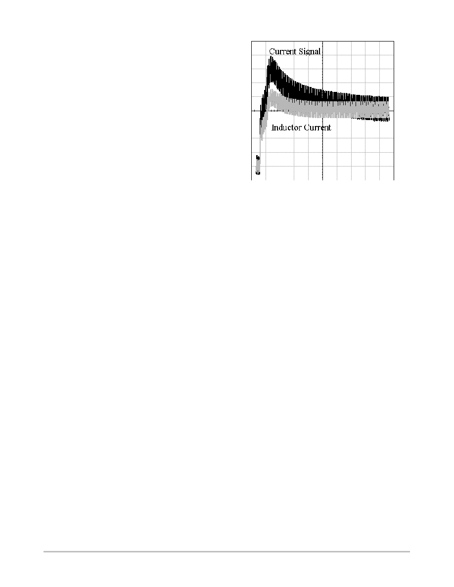
The waveforms in Figure 9 show a simulation of the
current sense signal and the actual inductor current during
a positive step in load current with values of L = 500 nH,
R
L
= 1.6 m
, R1 = 20 k and C1 = .01
µ
F. For ideal current
signal compensation the value of R1 should be 31 k
. Due
to the faster than ideal RC time constant there is an
overshoot of 50% and the overshoot decays with a 200
µ
s
time constant. With this compensation the I
LIM
pin
threshold must be set more than 50% above the full load
current to avoid triggering hiccup mode during a large
output load step.
Figure 9. Inductive Sensing waveform during a Step
with Fast RC Time Constant (50
m
s/div)
Current Limit
Two levels of overcurrent protection are provided. Any
time the voltage on a Current Sense pin exceeds CS
REF
by
more than the Single Phase Pulse by Pulse Current Limit, the
pwm comparator for that phase is turned off. This provides
fast peak current protection for individual phases. The
outputs of all the currents are also summed and filtered to
compare an averaged current signal to the voltage on the
I
LIM
pin. If this voltage is exceeded, the fault latch trips and
the SS capacitor is discharged by a 5
µ
A source until the
COMP pin reaches 0.2 V. Then soft≠start begins. The
converter will continue to operate in this mode until the fault
condition is corrected.
Overvoltage Protection
Overvoltage protection (OVP) is provided as a result of
the normal operation of the enhanced V
2
control topology
with synchronous rectifiers. The control loop responds to an
overvoltage condition within 400 ns, causing the top
MOSFET's to shut off, and the synchronous MOSFET's to
turn on. This results in a "crowbar" action to clamp the
output voltage and prevents damage to the load. The
regulator will remain in this state until the overvoltage
condition ceases or the input voltage is pulled low.
Transient Response and Adaptive Positioning
For applications with fast transient currents the output
filter is frequently sized larger than ripple currents require in

CS5323
http://onsemi.com
12
order to reduce voltage excursions during transients.
Adaptive voltage positioning can reduce peak≠peak output
voltage deviations during load transients and allow for a
smaller output filter. The output voltage can be set higher at
light loads to reduce output voltage sag when the load
current is stepped up and set lower during heavy loads to
reduce overshoot when the load current is stepped up. For
low current applications a droop resistor can provide fast
accurate adaptive positioning. However at high currents, the
loss in a droop resistor becomes excessive. For example; in
a 50 A converter a 1 m
resistor to provide a 50 mV change
in output voltage between no load and full load would
dissipate 2.5 Watts.
Lossless adaptive positioning is an alternative to using a
droop resistor, but must respond quickly to changes in load
current. Figure 10 shows how adaptive positioning works.
The waveform labeled normal shows a converter without
adaptive positioning. On the left, the output voltage sags
when the output current is stepped up and later overshoots
when current is stepped back down. With fast (ideal)
adaptive positioning the peak to peak excursions are cut in
half. In the slow adaptive positioning waveform the output
voltage is not repositioned quickly enough after current is
stepped up and the upper limit is exceeded.
Adaptive Positioning
Adaptive Positioning
Normal
Fast
Slow
Limits
Figure 10. Adaptive Positioning
The CS5323 uses two methods to provide fast and
accurate adaptive positioning. For low frequency
positioning the V
FB
and V
DRP
pins are used to adjust the
output voltage with varying load currents. For high
frequency positioning, the current sense input pins can be
used to control the power stage output impedance. The
transition between fast and slow positioning is adjusted by
the error amp compensation.
The CS5323 can be configured to adjust the output
voltage based on the output current of the converter. The
adaptive positioning circuit is designed to select the DAC
setting as the maximum output voltage. (Refer to Figure 1 on
page 2.)
To set the no≠load positioning a resistor (R9) is placed
between the output voltage and V
FB
pin. The V
FB
bias
current will develop a voltage across the resistor to decrease
the output voltage. The V
FB
bias current is dependent on the
value of ROSC. See Figure 4 on the datasheet.
During no load conditions the V
DRP
pin is at the same
voltage as the V
FB
pin, so none of the V
FB
bias current flows
through the V
DRP
resistor (R6). When output current
increases the V
DRP
pin increases proportionally and the
V
DRP
pin current offsets the V
FB
bias current and causes the
output voltage to further decrease.
The V
FB
and V
DRP
pins take care of the slower and DC
voltage positioning. The first few
µ
s are controlled primarily
by the ESR and ESL of the output filter. The transition
between fast and slow positioning is controlled by the ramp
size and the error amp compensation. If the ramp size is too
large or the error amp too slow there will be a long transition
to the final voltage after a transient. This will be most
apparent with lower capacitance output filters.
Note: Large levels of adaptive positioning can cause pulse
width jitter.
Error Amp Compensation
The transconductance error amplifier can be configured to
provide both a slow soft≠start and a fast transient response.
C4 in the main applications diagram controls soft≠start. A
0.1
µ
F capacitor with the 30
µ
A error amplifier output
capability will allow the output to ramp up at 0.3 V/ms or
1.5 V in 5 ms.
R10 is connected in series with C4 to allow the error
amplifier to slew quickly over a narrow range during load
transients. Here the 30
µ
A error amplifier output capability
works against 8 k
(R10) to limit the window of fast slewing
too 240 mV ≠ enough to allow for fast transients, but not
enough to interfere with soft≠start. This window will be
noticeable as a step in the COMP pin voltage at start≠up. The
size of this step must be kept smaller than the Channel
Start≠Up Offset (nominally 0.4 V) for proper soft≠start
operation. If adaptive positioning is used the R9 and R8 form
a divider with the V
DRP
end held at the DAC voltage during
start≠up, which effectively makes the Channel Start≠Up
Offset larger.
C12 is included for error amp stability. A capacitive load
is required on the error amp output. Use of values less than
1 nF may result in error amp oscillation of several MHz.
C11 and the parallel resistance of the V
FB
resistor (R9)
and the V
DRP
resistor (R6) are used to roll off the error amp
gain. C28 adds a zero to the error amp response to boost the
phase near the crossover frequency.
UVLO
The CS5323 has one undervoltage lockout function
connected to the V
CC
pin. In applications where the
converter is powered from multiple voltages, additional
UVLO protection might be required if the voltage powering
the controller can turn on before other voltages.
For the 12 V
IN
converter in Figure 1, the CS5323 UVLO
function monitors the 5.0 V supply. If the 5.0 V supply
comes up before the 12 V supply, the COMP pin will rise
until it reaches the upper rail or until the 12 V supply comes
up and the converter comes into regulation. If the delay
between the 5.0 V and 12 V supplies is too long, soft≠start
will be compromised. A diode connected from the 12 V
supply to the COMP pin can hold the COMP pin down until
the 12 V supply starts to come up. Or, if a higher UVLO
CS5323
http://onsemi.com
13
threshold is needed, a circuit like the one in Figure 11 will
lock out the converter until the 12 V supply reaches about
7.0 V.
Figure 11. External UVLO Circuit
COMP
100 k
100 k
50 k
+5 V
+12 V
Remote Sense
In some applications that require remote output voltage
sensing, there are conditions when the path of the feedback
signal can be broken. In a voltage regulator module (VRM)
the remote voltage feedback sense point is typically off the
module. If the module is powered apart from the intended
application, the feedback will be left open. On a
motherboard, the feedback path might be broken when the
processor socket is left open. Without the feedback
connection the output voltage is likely to exceed the
intended voltage. To protect the circuit from overvoltage
conditions, a resistor can be connected between the local
output voltage and the remote sense line as shown in Figure
12.
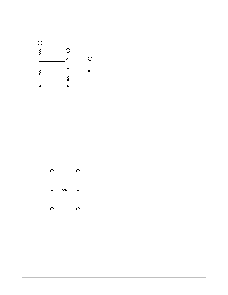
Figure 12. Remote Sense Connection
Local V
OUT
100
Remote V
OUT
Remote Sense Line
CS
REF
Network
V
FB
Network
Layout Guidelines
With the fast rise, high output currents of microprocessor
applications parasitic inductance and resistance should be
considered when laying out the power, filter and feedback
signal sections of the board. Typically a multi≠layer board
with at least one ground plane is recommended. If the layout
is such that high currents can exist in the ground plane
underneath the controller or control circuitry, the ground
plane can be slotted to reroute the currents away from the
controller. The slots should typically not be placed between
the controller and the output voltage or in the return path of
the gate drive. Additional power and ground planes or
islands can be added as required for a particular layout.
Output filter components should be placed on wide planes
connected directly to the load to minimize resistive drops
during heavy loads and inductive drops and ringing during
transients. If required, the planes for the output voltage and
return can be interleaved to minimize inductance between
the filter and load.
Voltage feedback should be taken from a point of the
output or the output filter that doesn't favor any one phase.
If the feedback connection is closer to one inductor than the
others the ripple associated with that phase may appear
larger than the ripple associated with the other phases and
poor current sharing can result.
The current sense signal is typically tens of milli≠volts.
Noise pick≠up should be avoided wherever possible.
Current feedback traces should be routed away from noisy
areas such as switch nodes and gate drive signals. The paths
should be matched as well as possible. It is especially
important that all current sense signals be picked off at
similar points for accurate current sharing. If the current
signal is taken from a place other than directly at the inductor
any additional resistance between the pick≠off point and the
inductor appears as part of the inherent inductor resistance
and should be considered in design calculations. Capacitors
for the current feedback networks should be placed as close
to the current sense pins as practical.
DESIGN PROCEDURE
Current Sensing, Power Stage and
Output Filter Components
1. Choose the output filter components to meet peak
transient requirements. The formula below can be
used to provide an approximate starting point for
capacitor choice, but will be inadequate to calculate
actual values.
D
VPEAK
+
(
D
I
D
T)
ESL
) D
I
ESR
Ideally the output filter should be simulated with
models including ESR, ESL, circuit board parasitics
and delays due to switching frequency and converter
response. Typically both bulk capacitance
(electrolytic, Oscon, etc,) and low impedance
capacitance (ceramic chip) will be required. The bulk
capacitance provides "hold up" during the converter
response. The low impedance capacitance reduces
steady state ripple and bypasses the bulk capacitance
during slewing of output current.
2. For inductive current sensing (only) choose the
current sense network RC to provide a 25 mV
minimum ramp during steady state operation.
R
+
(VIN
*
VOUT)
VOUT VIN
F
C
25 mV

CS5323
http://onsemi.com
14
Then choose the inductor value and inherent resistance
to satisfy L/R
L
= R
◊
C.
For ideal current sense compensation the ratio of L and
R
L
is fixed, so the values of L and R
L
will be a
compromise typically with the maximum value R
L
limited by conduction losses or inductor temperature
rise and the minimum value of L limited by ripple
current.
3. For resistive current sensing choose L and R
S
to
provide a steady state ramp greater than 25 mV.
L RS
+
(VIN
*
VOUT)
TON 25 mV
Again the ratio of L and R
L
is fixed and the values of
L and R
S
will be a compromise.
4. Calculate the high frequency output impedance
(ConverterZ) of the converter during transients. This
is the impedance of the Output filter ESR in parallel
with the power stage output impedance (PwrstgZ)
and will indicate how far from the original level
(
VR) the output voltage will typically recover to
within one switching cycle. For a good transient
response
VR should be less than the peak output
voltage overshoot or undershoot.
D
VR
+
ConverterZ
ESR
ConverterZ
+
PwrstgZ
ESR
PwrstgZ
)
ESR
where:
PwrstgZ
+
RS
CSA Gain 3
Multiply the converterZ by the output current step size
to calculate where the output voltage should recover to
within the first switching cycle after a transient. If the
ConverterZ is higher than the value required to recover
to where the adaptive positioning is set the remainder
of the recovery will be controlled by the error amp
compensation and will typically recover in 10 ≠ 20
µ
s.
D
VR
+ D
IOUT
ConverterZ
Make sure that
VR is less than the expected peak
transient for a good transient response.
5. Adjust L and R
L
or R
S
as required to meet the best
combination of transient response, steady state output
voltage ripple and pulse width jitter.
Current Limit
When the sum of the Current Sense amplifiers (V
ITOTAL
)
exceeds the voltage on the I
LIM
pin the part will enter hiccup
mode. For inductive sensing the I
LIM
pin voltage should be
set based on the inductor resistance (or current sense
resistor) at max temperature and max current. To set the level
of the I
LIM
pin:
6.
VI(LIM)
+
R
IOUT(LIM)
CS to ILIM Gain
where:
R is R
L
or R
S;
I
OUT(LIM)
is the current limit threshold.
For the overcurrent to work properly the inductor time
constant (L/R) should be
the Current sense RC. If the
RC is too fast, during step loads the current waveform
will appear larger than it is (typically for a few hundred
µ
s) and may trip the current limit at a level lower than
the DC limit.
Adaptive Positioning
7. To set the amount of voltage positioning below the
DAC setting at no load connect a resistor (R
V
(
FB
))
between the output voltage and the V
FB
pin. Choose
R
V
(
FB
) as;
RV(FB)
+
NL Position VFB Bias Current
See Figure 4 for V
FB
Bias Current.
8. To set the difference in output voltage between no load
and full load, connect a resistor (R
V(DRP)
) between the
V
DRP
and V
FB
pins. R
V(DRP)
can be calculated in two
steps. First calculate the difference between the V
DRP
and V
FB
pin at full load. (The V
FB
voltage should be
the same as the DAC voltage during closed loop
operation.) Then choose the R
V(DRP)
to source enough
current across R
V
(
FB
) for the desired change in output
voltage.
D
VV(DRP)
+
IOUTFL
R
CS to VDRP Gain
where:
R = R
L
or R
S
for one phase;
I
OUTFL
is the full load output current.
RV(DRP)
+ D
VDRP
RV(FB)
D
VOUT
Calculate Input Filter Capacitor Current Ripple
The procedure below assumes that phases do not overlap
and output inductor ripple current (P≠P) is less than the
average output current of one phase.
9. Calculate Input Current
IIN
+
VOUT
IOUT
(Efficiency
VIN)
10. Calculate Duty Cycle (per phase).
Duty Cycle
+
VOUT
(Efficiency
VIN)
11. Calculate Apparent Duty Cycle.
Apparent Duty Cycle
+
Duty Cycle
# of Phases
12. Calculate Input Filter Capacitor Ripple Current. Use
the chart in Figure 13 to calculate the normalized
ripple current (K
RMS
) based on the reciprocal of
Apparent Duty Cycle. Then multiply the input current
by K
RMS
to obtain the Input Filter Capacitor Ripple
Current.
Ripple (RMS)
+
IIN
KRMS

CS5323
http://onsemi.com
15
4.00
3.50
3.00
2.50
2.00
1.50
1.00
0.50
0.00
1/ Apparent Duty Cycle
Frequency
, kHz
15
10
5
0
Figure 13. Normalized Input Filter Capacitor
Ripple Current
DESIGN EXAMPLE
Choose the component values for lossless current sensing,
adaptive positioning and current limit for a 12 V to 1.5 V 60
A converter. The adaptive positioning is chosen 20 mV
below the maximum V
OUT
at no load and 70 mV below the
no≠load position with 60 A out. The peak output voltage
transient is 100 mV max during a 60 A step current. The
overcurrent limit is nominally 75 A.
Current Sensing, Power Stage
and Output Filter Components
1. Assume 1.5 m
of output filter ESR.
R
+
(VIN
*
VOUT)
(VOUT VIN) (F
C
25 mV)
+
(12
*
1.5)
(1.5 12) (250 k
.01
m
F
25 mV)
+
21 k
W Â
Choose 20 k
W
L RL
+
.01
m
F
20 k
W +
200
m
s
Choose RL
+
2.0 m
W
L
+
2 m
W
200
m
s
+
400 nH
2
.
3. n/a
PwrstgZ
+
RL
CSA Gain 3
+
1.5 m
W
4.2 3
+
2.1 m
W
ConverterZ
+
PwrstgZ
ESR
PwrstgZ
)
ESR
+
2.8 m
W
1.5 m
W
2.8 m
W )
1.5 m
W
^
1.0 m
W
D
VR
+
1.0 m
W
60 A
+
60 mV
4.
5. n/a
Current Limit
VI(LIM)
+
RL
IOUT(LIM)
CS to ILIM Gain
+
1.5 m
W
75 A
6.5
+
731 mV
6.
Adaptive Positioning
RV(FB)
+
NL Position VFB Bias Current
+
20 mV 19
m
A
^
1.00 k
W
7.
D
VDRP
+
RL
IOUT
Current Sense to VDRP Gain
+
2 m
W
60 A
3
+
360 mV
RV(DRP)
+ D
VDRP
RV(FB)
D
VOUT
+
360 mV
1.00 k
W
50 mV
+
7.2 k
W
8.
IIN
+
1.6 V
60 A
(0.85
12VIN)
+
9.4 A
9.
Duty Cycle
+
1.6 V
(0.85
12 VIN)
+
0.16
10.
Apparent Duty Cycle
+
0.16
3.0
+
0.48
11.
RMS ripple is 9.4 A
1.0
+
9.4 A
12.

CS5323
http://onsemi.com
16
PACKAGE DIMENSIONS
20
1
11
10
B
20X
H
10X
C
L
18X
A1
A
SEATING
PLANE
q
h
X 45
_
E
D
M
0.25
M
B
M
0.25
S
A
S
B
T
e
T
B
A
DIM
MIN
MAX
MILLIMETERS
A
2.35
2.65
A1
0.10
0.25
B
0.35
0.49
C
0.23
0.32
D
12.65
12.95
E
7.40
7.60
e
1.27 BSC
H
10.05
10.55
h
0.25
0.75
L
0.50
0.90
q
0
7
NOTES:
1. DIMENSIONS ARE IN MILLIMETERS.
2. INTERPRET DIMENSIONS AND TOLERANCES
PER ASME Y14.5M, 1994.
3. DIMENSIONS D AND E DO NOT INCLUDE MOLD
PROTRUSION.
4. MAXIMUM MOLD PROTRUSION 0.15 PER SIDE.
5. DIMENSION B DOES NOT INCLUDE DAMBAR
PROTRUSION. ALLOWABLE PROTRUSION SHALL
BE 0.13 TOTAL IN EXCESS OF B DIMENSION AT
MAXIMUM MATERIAL CONDITION.
_
_
SO≠20L
DW SUFFIX
CASE 751D≠05
ISSUE F
PACKAGE THERMAL DATA
Parameter
SO≠20L
Unit
R
JC
Typical
17
∞
C/W
R
JA
Typical
90
∞
C/W
ON Semiconductor and are registered trademarks of Semiconductor Components Industries, LLC (SCILLC). SCILLC reserves the right to make
changes without further notice to any products herein. SCILLC makes no warranty, representation or guarantee regarding the suitability of its products for any
particular purpose, nor does SCILLC assume any liability arising out of the application or use of any product or circuit, and specifically disclaims any and all
liability, including without limitation special, consequential or incidental damages. "Typical" parameters which may be provided in SCILLC data sheets and/or
specifications can and do vary in different applications and actual performance may vary over time. All operating parameters, including "Typicals" must be
validated for each customer application by customer's technical experts. SCILLC does not convey any license under its patent rights nor the rights of others.
SCILLC products are not designed, intended, or authorized for use as components in systems intended for surgical implant into the body, or other applications
intended to support or sustain life, or for any other application in which the failure of the SCILLC product could create a situation where personal injury or death
may occur. Should Buyer purchase or use SCILLC products for any such unintended or unauthorized application, Buyer shall indemnify and hold SCILLC
and its officers, employees, subsidiaries, affiliates, and distributors harmless against all claims, costs, damages, and expenses, and reasonable attorney fees
arising out of, directly or indirectly, any claim of personal injury or death associated with such unintended or unauthorized use, even if such claim alleges that
SCILLC was negligent regarding the design or manufacture of the part. SCILLC is an Equal Opportunity/Affirmative Action Employer.
PUBLICATION ORDERING INFORMATION
JAPAN: ON Semiconductor, Japan Customer Focus Center
2≠9≠1 Kamimeguro, Meguro≠ku, Tokyo, Japan 153≠0051
Phone: 81≠3≠5773≠3850
Email: r14525@onsemi.com
ON Semiconductor Website: http://onsemi.com
For additional information, please contact your local
Sales Representative.
CS5323/D
V
2
is a trademark of Switch Power, Inc.
Literature Fulfillment:
Literature Distribution Center for ON Semiconductor
P.O. Box 5163, Denver, Colorado 80217 USA
Phone: 303≠675≠2175 or 800≠344≠3860 Toll Free USA/Canada
Fax: 303≠675≠2176 or 800≠344≠3867 Toll Free USA/Canada
Email: ONlit@hibbertco.com
N. American Technical Support: 800≠282≠9855 Toll Free USA/Canada