 | –≠–ª–µ–∫—Ç—Ä–æ–Ω–Ω—ã–π –∫–æ–º–ø–æ–Ω–µ–Ω—Ç: CS8182 | –°–∫–∞—á–∞—Ç—å:  PDF PDF  ZIP ZIP |
©
Semiconductor Components Industries, LLC, 2004
August, 2004 - Rev. 21
1
Publication Order Number:
CS8182/D
CS8182
Micropower 200 mA
Low Dropout Tracking
Regulator/Line Driver
The CS8182 is a monolithic integrated low dropout tracking
regulator designed to provide adjustable buffered output voltage that
closely tracks (
±
10 mV) the reference input. The output delivers up to
200 mA while being able to be configured higher, lower or equal to the
reference voltages.
The output has been designed to operate over a wide range (2.8 V to
45 V) while still maintaining excellent DC characteristics. The
CS8182 is protected from reverse battery, short circuit and thermal
runaway conditions. The device also can withstand 45 V load dump
transients and -50 V reverse polarity input voltage transients. This
makes it suitable for use in automotive environments.
The V
REF
/ENABLE lead serves two purposes. It is used to provide
the input voltage as a reference for the output and it also can be pulled
low to place the device in sleep mode where it nominally draws less
than 30
mA from the supply.
Features
∑
200 mA Source Capability
∑
Output Tracks within
±
10 mV Worst Case
∑
Low Dropout (0.35 V Typ. @ 200 mA)
∑
Low Quiescent Current
∑
Thermal Shutdown
∑
Short Circuit Protection
∑
Wide Operating Range
∑
Internally Fused Leads in SO-8 Package
∑
For Automotive and Other Applications Requiring Site and Change
Control
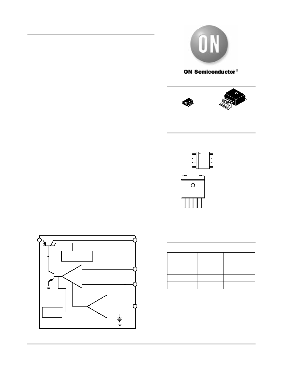
Current Limit &
SAT Sense
+
-
ENABLE
+
-
Thermal
Shutdown
2.0 V
V
OUT
Adj
V
REF
/ENABLE
GND
V
IN
Figure 1. Block Diagram
A
= Assembly Location
WL, L
= Wafer Lot
YY, Y
= Year
WW, W
= Work Week
PIN CONNECTIONS AND
MARKING DIAGRAMS
SO-8
DF SUFFIX
CASE 751
D
2
PAK-5
DPS SUFFIX
CASE 936AC
V
IN
V
OUT
8182
1
GND
GND
Adj
GND
GND
V
REF
/ENABLE
AL
YW
Device
Package
Shipping
ORDERING INFORMATION*
CS8182YDF8
SO-8
95 Units/Rail
CS8182YDFR8
SO-8
CS8182YDPS5
D
2
PAK 5-PIN
2500 Tape & Reel
CS8182YDPSR5
*Consult your local sales representative for SO-8 with
exposed pads package option.
D
2
PAK 5-PIN
750 Tape & Reel
50 Units/Rail
CS8182
AWLYWW
1
Tab
GND
Pin 1. V
IN
2. V
OUT
3. GND
4. Adj
5. V
REF
1
5
1
8
http://onsemi.com
For information on tape and reel specifications,
including part orientation and tape sizes, please
refer to our Tape and Reel Packaging Specifications
Brochure, BRD8011/D.
CS8182
http://onsemi.com
2
PACKAGE PIN DESCRIPTION
Package Lead Number
SO-8
D
2
PAK 5-PIN
Lead Symbol
Function
8
1
V
IN
Input voltage.
1
2
V
OUT
Regulated output.
2, 3, 6, 7
3
GND
Ground.
4
4
Adj
Adjust lead.
5
5
V
REF
/ENABLE
Reference voltage and ENABLE input.
MAXIMUM RATINGS
Rating
Value
Unit
Storage Temperature
-65 to 150
∞
C
Supply Voltage Range (continuous)
-15 to 45
V
Supply Voltage Range (normal, continuous)
3.4 to 45
V
Peak Transient Voltage (V
IN
= 14 V, Load Dump Transient = 31 V)
45
V
Voltage Range (Adj, V
OUT
, V
REF
/ENABLE)
-10 to 45
V
Maximum Junction Temperature
150
∞
C
Package Thermal Resistance, SO-8:
Junction-to-Case, R
q
JC
Junction-to-Ambient, R
q
JA
25
110
∞
C/W
∞
C/W
Package Thermal Resistance, D
2
PAK, 5-Pin:
Junction-to-Case, R
q
JC
Junction-to-Ambient, R
q
JA
4.0
10-50**
∞
C/W
∞
C/W
ESD Capability (Human Body Model)
(Machine Model)
2.0
200
kV
V
Lead Temperature Soldering:
Reflow: (SO-8)
(Note 1)
(D2PAK)
240 peak
225 peak
(Note 2)
∞
C
Maximum ratings are those values beyond which device damage can occur. Maximum ratings applied to the device are individual stress limit
values (not normal operating conditions) and are not valid simultaneously. If these limits are exceeded, device functional operation is not implied,
damage may occur and reliability may be affected.
1. 60 second maximum above 183
∞
C.
2. -5
∞
C/+0
∞
C allowable conditions.
*Depending on thermal properties of substrate. R
q
JA
= R
q
JC
+ R
q
CA
CS8182
http://onsemi.com
3
ELECTRICAL CHARACTERISTICS
(V
IN
= 14 V; V
REF
/ENABLE > 2.75 V; -40
∞
C < T
J
< +125
∞
C; C
OUT
10
m
F;
0.1
W
< C
OUT-ESR
< 1.0
W
@ 10 kHz, unless otherwise specified.)
Parameter
Test Conditions
Min
Typ
Max
Unit
Regular Output
V
REF
- V
OUT
V
OUT
Tracking Error
4.5 V
V
IN
26 V, 100
m
A
I
OUT
200 mA, Note 3
V
IN
= 12 V, I
OUT
= 30 mA, V
REF
= 5.0 V, Note 3
-10
-5.0
-
-
10
5
mV
mV
Dropout Voltage (V
IN
- V
OUT
)
I
OUT
= 100
m
A
I
OUT
= 30 mA
I
OUT
= 200 mA
-
-
-
100
-
350
150
500
600
mV
mV
mV
Line Regulation
4.5 V
V
IN
26 V, Note 3
-
-
10
mV
Load Regulation
100
m
A
I
OUT
200 mA, Note 3
-
-
10
mV
Adj Lead Current
Loop in Regulation
-
0.2
1.0
m
A
Current Limit
V
IN
= 14 V, V
REF
= 5.0 V, V
OUT
= 90% of V
REF
, Note 3
225
-
700
mA
Quiescent Current (I
IN
- I
OUT
)
V
IN
= 12 V, I
OUT
= 200 mA
V
IN
= 12 V, I
OUT
= 100
m
A
V
IN
= 12 V, V
REF
/ENABLE = 0 V
-
-
-
15
75
30
25
150
55
mA
m
A
m
A
Reverse Current
V
OUT
= 5.0 V, V
IN
= 0 V
-
0.2
1.5
mA
Ripple Rejection
f = 120 Hz, I
OUT
= 200 mA, 4.5 V
V
IN
26 V
60
-
-
dB
Thermal Shutdown
GBD
150
180
210
∞
C
V
REF
/ENABLE
Enable Voltage
-
0.80
2.00
2.75
V
Input Bias Current
V
REF
/ENABLE
-
0.2
1.0
m
A
3. V
OUT
connected to Adj lead.
CS8182
http://onsemi.com
4
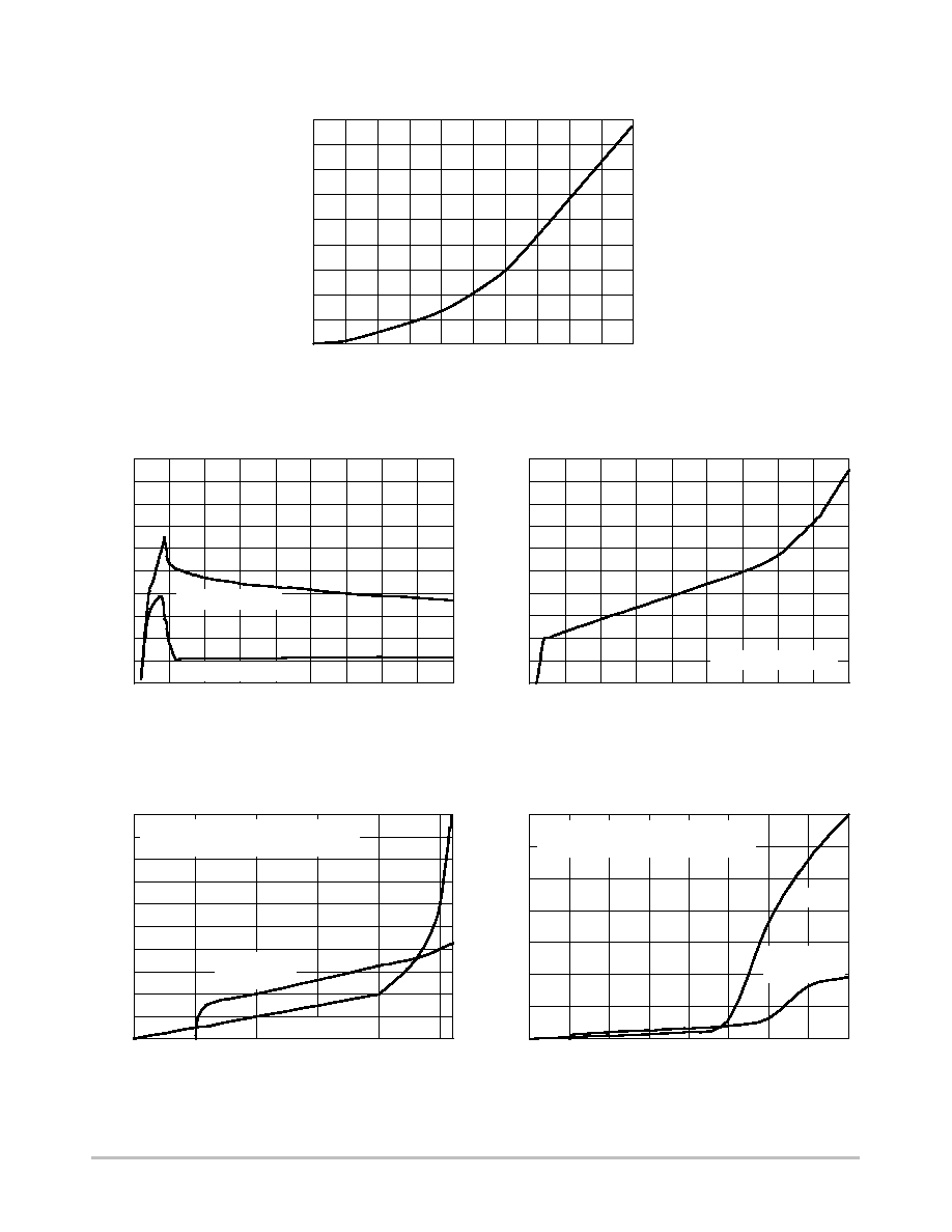
TYPICAL CHARACTERISTICS
18
16
14
12
10
8
6
4
2
0
Figure 2. Quiescent Current vs. Output Current
0
20
40
60
80
100
120 140 160 180 200
OUTPUT CURRENT (mA)
QUIESCENT CURRENT (mA)
Figure 3. Quiescent Current vs. Input Voltage
(Operating Mode)
1
0.9
0.8
0.7
0.6
0.5
0.3
0.2
0.1
0
0
5
10
15
20
25
30
35
40
45
V
IN
, INPUT VOLTAGE (V)
QUIESCENT CURRENT (mA)
0.4
Figure 4. Quiescent Current vs. Input Voltage
(Sleep Mode)
Figure 5. V
OUT
Reverse Current
Figure 6. V
OUT
Reverse Current
100
90
80
70
60
50
30
20
10
0
0
5
10
15
20
25
30
35
40
45
V
IN
, INPUT VOLTAGE (V)
QUIESCENT CURRENT (
m
A)
40
20
18
16
14
12
10
6
4
2
0
0
5
10
15
20
25
FORCED V
OUT
VOLTAGE (V)
CURRENT INT
O V
OUT
(mA)
8
140
120
100
80
60
40
20
0
0
5
10
15
20
25
FORCED V
OUT
VOLTAGE (V)
CURRENT INT
O V
OUT
(mA)
30
35
40
I (V
OUT
) = 20 mA
I (V
OUT
) = 1 mA
V
REF
/ ENABLE = 0 V
V
IN
= 6 V*
V
REF
= 5 V**
V
IN
= 0 V
* Graph is duplicate for V
IN
> 1.6 V.
**Dip (@5 V) shifts with V
REF
voltage.
V
IN
= 6 V*
V
REF
= 5 V**
V
IN
= 0 V
* Graph is duplicate for V
IN
> 1.6 V.
**Dip (@5 V) shifts with V
REF
voltage.
CS8182
http://onsemi.com
5
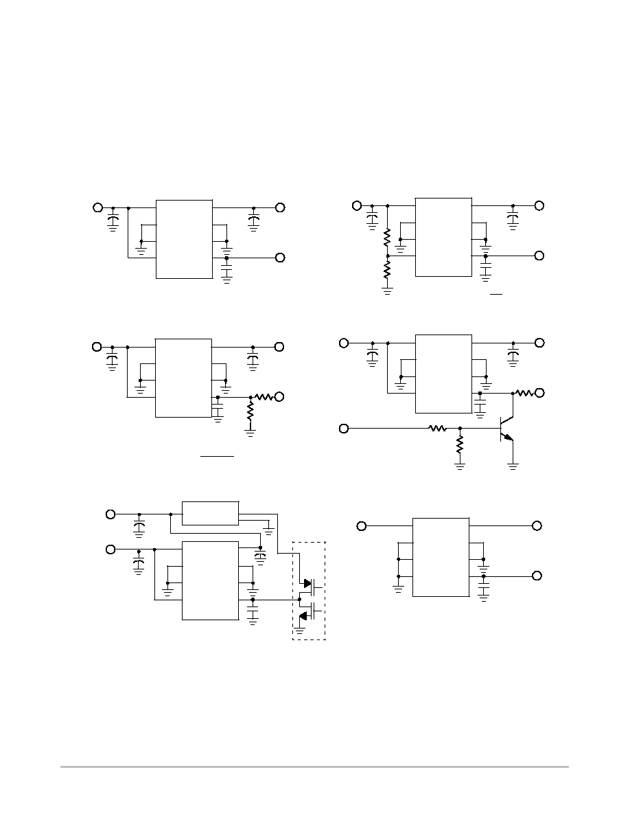
CIRCUIT DESCRIPTION
ENABLE Function
By pulling the V
REF
/ENABLE lead below 2.0 V typically,
(see Figure 10 or Figure 11), the IC is disabled and enters a
sleep state where the device draws less than 55
mA from
supply. When the V
REF
/ENABLE lead is greater than 2.75 V,
V
OUT
tracks the V
REF
/ENABLE lead normally.
Output Voltage
The output is capable of supplying 200 mA to the load
while configured as a similar (Figure 7), lower (Figure 9), or
higher (Figure 8) voltage as the reference lead. The Adj lead
acts as the inverting terminal of the op amp and the V
REF
lead as the non-inverting.
The device can also be configured as a high-side driver as
displayed in Figure 12.
Figure 7. Tracking Regulator at the Same Voltage
V
IN
V
OUT
GND
GND
V
REF
/
GND
GND
Adj
ENABLE
Loads
5.0 V
B+
C1*
1.0
m
F
C2**
10
m
F
V
OUT
, 200 mA
VOUT
+
VREF
Figure 8. Tracking Regulator at Higher Voltages
V
IN
V
OUT
GND
GND
V
REF
/
GND
GND
Adj
ENABLE
Loads
V
REF
B+
C1*
1.0
m
F
C2**
10
m
F
V
OUT
, 200 mA
R
A
R
F
VOUT
+
VREF(1
)
RE
RA
)
CS8182
CS8182
C3***
10 nF
C3***
10 nF
Figure 9. Tracking Regulator at Lower Voltages
V
IN
V
OUT
GND
GND
V
REF
/
GND
GND
Adj
ENABLE
Loads
V
REF
B+
C1*
1.0
m
F
C2**
10
m
F
V
OUT
, 200 mA
VOUT
+
VREF(
R2
R1
)
R2
)
R2
R1
Figure 10. Tracking Regulator with ENABLE Circuit
V
IN
V
OUT
GND
GND
V
REF
/
GND
GND
Adj
ENABLE
from MCU
V
REF
B+
C1*
1.0
m
F
C2**
10
m
F
V
OUT
, 200 mA
R
CS8182
CS8182
C3***
10 nF
C3***
10 nF
Figure 11. Alternative ENABLE Circuit
V
IN
V
OUT
GND
GND
V
REF
/
GND
GND
Adj
ENABLE
10
m
F
Figure 12. High-Side Driver
V
IN
V
OUT
GND
GND
V
REF
/
GND
GND
Adj
ENABLE
MCU
B+
200 mA
VOUT
+
B
) *
VSAT
** C2 is required for stability.
* C1 is required if the regulator is far from the power source filter.
CS8182
CS8182
5.0 V
I/O
NCV8501
6.0 V-40 V
V
IN
100 nF
V
REF
(5.0 V)
m
C
To Load
(e.g. sensor)
C1*
1.0
m
F
C3***
10 nF
C3***
10 nF
*** C3 is recommended for EMC susceptibility.
CS8182
http://onsemi.com
6
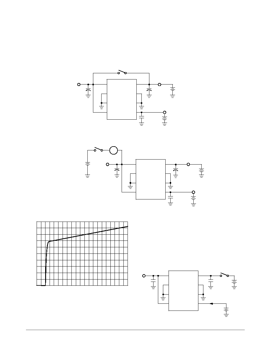
APPLICATION NOTES
V
OUT
Short to Battery
The CS8182 will survive a short to battery when hooked
up the conventional way as shown in Figure 13. No damage
to the part will occur. The part also endures a short to battery
when powered by an isolated supply at a lower voltage as in
Figure 14. In this case the CS8182 supply input voltage is set
at 7 V when a short to battery (14 V typical) occurs on V
OUT
which normally runs at 5 V. The current into the device
(ammeter in Figure 14) will draw additional current as
displayed in Figure 15.
V
OUT
GND
GND
Adj
V
IN
GND
GND
V
REF
/
ENABLE
V
OUT
5.0 V
70 mA
C1*
1.0
m
F
Automotive Battery
typically 14 V
Short to battery
CS8182
Figure 13.
C2**
10
m
F
V
OUT
GND
GND
Adj
V
IN
GND
GND
V
REF
/
ENABLE
V
OUT
C1*
1.0
m
F
CS8182
Figure 14.
C2**
10
m
F
C3***
10 nF
V
OUT
= V
REF
5.0 V
Loads
B+
5.0 V
70 mA
Automotive Battery
typically 14 V
Short to battery
V
OUT
= V
REF
5.0 V
Loads
B+
C3***
10 nF
A
7 V
** C2 is required for stability.
* C1 is required if the regulator is far from the power source filter.
*** C3 is recommended for EMC susceptibility.
+
-
+
-
+
-
+
-
Figure 15. V
OUT
Short to Battery
2.0
1.8
1.6
1.4
1.2
1.0
0.6
0.4
0.2
0
6
5
10
15
20
25
V
OUT
VOLTAGE (V)
CURRENT (mA)
0.8
7 8 9
1112 1314
1617 1819
2122 2324
26
Switched Application
The CS8182 has been designed for use in systems where
the reference voltage on the V
REF
/ENABLE pin is
continuously on. Typically, the current into the
V
REF
/ENABLE pin will be less than 1.0
mA when the
voltage on the V
IN
pin (usually the ignition line) has been
switched out (V
IN
can be at high impedance or at ground.)
Reference Figure 16.
V
OUT
GND
GND
Adj
V
IN
GND
GND
V
REF
/
ENABLE
V
OUT
V
REF
5.0 V
V
BAT
C1
1.0
m
F
Ignition
Switch
< 1.0
m
A
CS8182
Figure 16.
C2
10
m
F

CS8182
http://onsemi.com
7
External Capacitors
The output capacitor for the CS8182 is required for
stability. Without it, the regulator output will oscillate.
Actual size and type may vary depending upon the
application load and temperature range. Capacitor effective
series resistance (ESR) is also a factor in the IC stability.
Worst-case is determined at the minimum ambient
temperature and maximum load expected.
The output capacitor can be increased in size to any
desired value above the minimum. One possible purpose of
this would be to maintain the output voltage during brief
conditions of negative input transients that might be
characteristic of a particular system.
The capacitor must also be rated at all ambient
temperatures expected in the system. To maintain regulator
stability down to -40
∞
C, a capacitor rated at that temperature
must be used.
More information on capacitor selection for SMART
REGULATOR
Æ
s is available in the SMART REGULATOR
application note, "Compensation for Linear Regulators,"
document number SR003AN/D, available through our
website at http://www.onsemi.com.
Calculating Power Dissipation in a Single Output
Linear Regulator
The maximum power dissipation for a single output
regulator (Figure 17) is:
PD(max)
+
{VIN(max)
*
VOUT(min)} IOUT(max)
)
VIN(max)IQ
(1)
where:
V
IN(max)
is the maximum input voltage,
V
OUT(min)
is the minimum output voltage,
I
OUT(max)
is the maximum output current, for the
application,and
I
Q
is the quiescent current the regulator consumes at
I
OUT(max)
.
Once the value of PD(max) is known, the maximum
permissible value of R
qJA
can be calculated:
R
q
JA
+
150
∞
C
*
TA
PD
(2)
The value of R
qJA
can then be compared with those in the
package section of the data sheet. Those packages with
R
qJA
's less than the calculated value in equation 2 will keep
the die temperature below 150
∞
C.
In some cases, none of the packages will be sufficient to
dissipate the heat generated by the IC, and an external heat
sink will be required.
Figure 17. Single Output Regulator with Key
Performance Parameters Labeled
I
IN
I
OUT
I
Q
SMART
V
OUT
V
IN
REGULATOR
Æ
Control
Features
Heatsinks
A heatsink effectively increases the surface area of the
package to improve the flow of heat away from the IC and
into the surrounding air.
Each material in the heat flow path between the IC and the
outside environment will have a thermal resistance. Like
series electrical resistances, these resistances are summed to
determine the value of R
qJA:
R
q
JA
+
R
q
JC
)
R
q
CS
)
R
q
SA
(3)
where:
R
qJC
= the junction-to-case thermal resistance,
R
qCS
= the case-to-heatsink thermal resistance, and
R
qSA
= the heatsink-to-ambient thermal resistance.
R
qJC
appears in the package section of the data sheet. Like
R
qJA
, it is a function of package type. R
qCS
and R
qSA
are
functions of the package type, heatsink and the interface
between them. These values appear in heat sink data sheets
of heatsink manufacturers.
CS8182
http://onsemi.com
8
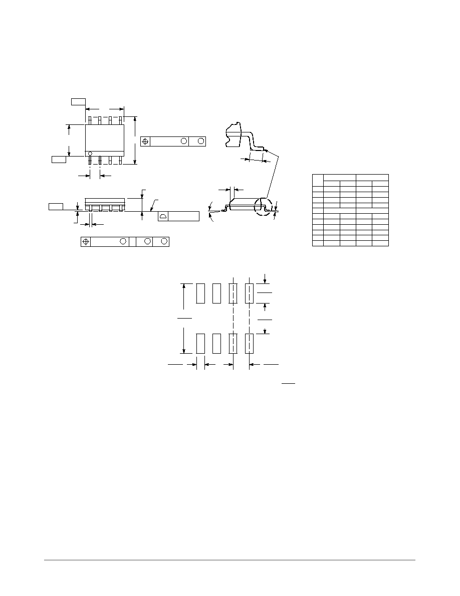
PACKAGE DIMENSIONS
SOIC-8
DF SUFFIX
CASE 751-07
ISSUE AB
SEATING
PLANE
1
4
5
8
N
J
X 45
_
K
NOTES:
1. DIMENSIONING AND TOLERANCING PER ANSI
Y14.5M, 1982.
2. CONTROLLING DIMENSION: MILLIMETER.
3. DIMENSION A AND B DO NOT INCLUDE MOLD
PROTRUSION.
4. MAXIMUM MOLD PROTRUSION 0.15 (0.006) PER
SIDE.
5. DIMENSION D DOES NOT INCLUDE DAMBAR
PROTRUSION. ALLOWABLE DAMBAR
PROTRUSION SHALL BE 0.127 (0.005) TOTAL IN
EXCESS OF THE D DIMENSION AT MAXIMUM
MATERIAL CONDITION.
6. 751-01 THRU 751-06 ARE OBSOLETE. NEW
STANDARD IS 751-07.
A
B
S
D
H
C
0.10 (0.004)
DIM
A
MIN
MAX
MIN
MAX
INCHES
4.80
5.00
0.189
0.197
MILLIMETERS
B
3.80
4.00
0.150
0.157
C
1.35
1.75
0.053
0.069
D
0.33
0.51
0.013
0.020
G
1.27 BSC
0.050 BSC
H
0.10
0.25
0.004
0.010
J
0.19
0.25
0.007
0.010
K
0.40
1.27
0.016
0.050
M
0
8
0
8
N
0.25
0.50
0.010
0.020
S
5.80
6.20
0.228
0.244
-X-
-Y-
G
M
Y
M
0.25 (0.010)
-Z-
Y
M
0.25 (0.010)
Z
S
X
S
M
_
_
_
_
Figure 18. SOIC-8
1.52
0.060
7.0
0.275
0.6
0.024
1.270
0.050
4.0
0.155
mm
inches
SCALE 6:1
SOLDERING FOOTPRINT
CS8182
http://onsemi.com
9
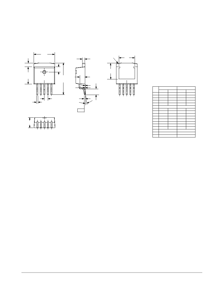
PACKAGE DIMENSIONS
D
2
PAK-5
DP SUFFIX
CASE 936AC-01
ISSUE O
DIM
MIN
MAX
MIN
MAX
MILLIMETERS
INCHES
A
0.396
0.406
10.05
10.31
B
0.330
0.340
8.38
8.64
C
0.170
0.180
4.31
4.57
D
0.026
0.036
0.66
0.91
E
0.045
0.055
1.14
1.40
G
0.067 REF
1.70 REF
H
0.580
0.620
14.73
15.75
K
0.055
0.066
1.40
1.68
L
0.000
0.010
0.00
0.25
M
0.098
0.108
2.49
2.74
N
0.017
0.023
0.43
0.58
NOTES:
1. DIMENSIONS AND TOLERANCING PER
ANSI Y14.5M, 1982.
2. CONTROLLING DIMENSION: INCH.
3. PACKAGE OUTLINE EXCLUSIVE OF
MOLD FLASH AND METAL BURR.
4. PACKAGE OUTLINE INCLUSIVE OF
PLATING THICKNESS.
5. FOOT LENGTH MEASURED AT
INTERCEPT POINT BETWEEN DATUM A
AND LEAD SURFACE.
C
E
P
N
M
W
R
L
-A-
A
B
H
K
D
G
S
U
V
P
0.090
0.110
2.29
2.79
R
0
8
S
0.095
0.105
2.41
2.67
U
0.30 REF
7.62 REF
V
0.305 REF
7.75 REF
W
0.010
0.25
_
_
0
8
_
_
TERMINAL 6
CS8182
http://onsemi.com
10
ON Semiconductor and are registered trademarks of Semiconductor Components Industries, LLC (SCILLC). SCILLC reserves the right to make changes without further notice
to any products herein. SCILLC makes no warranty, representation or guarantee regarding the suitability of its products for any particular purpose, nor does SCILLC assume any liability
arising out of the application or use of any product or circuit, and specifically disclaims any and all liability, including without limitation special, consequential or incidental damages.
"Typical" parameters which may be provided in SCILLC data sheets and/or specifications can and do vary in different applications and actual performance may vary over time. All
operating parameters, including "Typicals" must be validated for each customer application by customer's technical experts. SCILLC does not convey any license under its patent rights
nor the rights of others. SCILLC products are not designed, intended, or authorized for use as components in systems intended for surgical implant into the body, or other applications
intended to support or sustain life, or for any other application in which the failure of the SCILLC product could create a situation where personal injury or death may occur. Should
Buyer purchase or use SCILLC products for any such unintended or unauthorized application, Buyer shall indemnify and hold SCILLC and its officers, employees, subsidiaries, affiliates,
and distributors harmless against all claims, costs, damages, and expenses, and reasonable attorney fees arising out of, directly or indirectly, any claim of personal injury or death
associated with such unintended or unauthorized use, even if such claim alleges that SCILLC was negligent regarding the design or manufacture of the part. SCILLC is an Equal
Opportunity/Affirmative Action Employer. This literature is subject to all applicable copyright laws and is not for resale in any manner.
PUBLICATION ORDERING INFORMATION
N. American Technical Support: 800-282-9855 Toll Free
USA/Canada
Japan: ON Semiconductor, Japan Customer Focus Center
2-9-1 Kamimeguro, Meguro-ku, Tokyo, Japan 153-0051
Phone: 81-3-5773-3850
CS8182/D
SMART REGULATOR is a registered trademark of Semiconductor Components Industries, LLC (SCILLC).
LITERATURE FULFILLMENT:
Literature Distribution Center for ON Semiconductor
P.O. Box 5163, Denver, Colorado 80217 USA
Phone: 303-675-2175 or 800-344-3860 Toll Free USA/Canada
Fax: 303-675-2176 or 800-344-3867 Toll Free USA/Canada
Email: orderlit@onsemi.com
ON Semiconductor Website: http://onsemi.com
Order Literature: http://www.onsemi.com/litorder
For additional information, please contact your
local Sales Representative.