Complementary Silicon Power
Transistors
. . . for general purpose power amplification and switching such as
output or driver stages in applications such as switching regulators,
converters and power amplifiers.
╖
Low Collector¡Emitter Saturation Voltage
V
CE(sat)
= 1.0 V (Max) @ 8.0 A
╖
Fast Switching Speeds
╖
Complementary Pairs Simplifies Designs
╬╬╬╬╬╬╬╬╬╬╬╬╬╬╬╬╬╬╬╬╬╬╬
╬
╬╬╬╬╬╬╬╬╬╬╬╬╬╬╬╬╬╬╬╬╬
╬
╬╬╬╬╬╬╬╬╬╬╬╬╬╬╬╬╬╬╬╬╬╬╬
MAXIMUM RATINGS
╬╬╬╬╬╬╬╬╬╬╬╬
╬
╬╬╬╬╬╬╬╬╬╬
╬
╬╬╬╬╬╬╬╬╬╬╬╬
╬╬╬
╬
╬
╬
╬╬╬
╬╬╬╬╬╬╬╬
╬
╬╬╬╬╬╬
╬
╬╬╬╬╬╬╬╬
D44H or D45H
╬╬╬
╬
╬
╬
╬╬╬
╬╬╬╬╬╬╬╬╬╬╬╬
╬
╬╬╬╬╬╬╬╬╬╬
╬
╬╬╬╬╬╬╬╬╬╬╬╬
Rating
╬╬╬
╬
╬
╬
╬╬╬
Symbol
╬╬╬╬╬
╬
╬╬╬
╬
╬╬╬╬╬
8
╬╬╬╬
╬
╬╬
╬
╬╬╬╬
10, 11
╬╬╬
╬
╬
╬
╬╬╬
Unit
╬╬╬╬╬╬╬╬╬╬╬╬
╬
╬╬╬╬╬╬╬╬╬╬
╬
╬╬╬╬╬╬╬╬╬╬╬╬
Collector¡Emitter Voltage
╬╬╬
╬
╬
╬
╬╬╬
V
CEO
╬╬╬╬╬
╬
╬╬╬
╬
╬╬╬╬╬
60
╬╬╬╬
╬
╬╬
╬
╬╬╬╬
80
╬╬╬
╬
╬
╬
╬╬╬
Vdc
╬╬╬╬╬╬╬╬╬╬╬╬
╬
╬╬╬╬╬╬╬╬╬╬
╬
╬╬╬╬╬╬╬╬╬╬╬╬
Emitter Base Voltage
╬╬╬
╬
╬
╬
╬╬╬
V
EB
╬╬╬╬╬╬╬╬
╬
╬╬╬╬╬╬
╬
╬╬╬╬╬╬╬╬
5.0
╬╬╬
╬
╬
╬
╬╬╬
Vdc
╬╬╬╬╬╬╬╬╬╬╬╬
╬
╬╬╬╬╬╬╬╬╬╬
╬
╬╬╬╬╬╬╬╬╬╬╬╬
Collector Current -- Continuous
-- Peak (1)
╬╬╬
╬
╬
╬
╬╬╬
I
C
╬╬╬╬╬╬╬╬
╬
╬╬╬╬╬╬
╬
╬╬╬╬╬╬╬╬
10
20
╬╬╬
╬
╬
╬
╬╬╬
Adc
╬╬╬╬╬╬╬╬╬╬╬╬
╬
╬╬╬╬╬╬╬╬╬╬
╬
╬
╬╬╬╬╬╬╬╬╬╬
╬
╬╬╬╬╬╬╬╬╬╬╬╬
Total Power Dissipation
@ T
C
= 25
_
C
@ T
A
= 25
_
C
╬╬╬
╬
╬
╬
╬
╬
╬
╬╬╬
P
D
╬╬╬╬╬╬╬╬
╬
╬╬╬╬╬╬
╬
╬
╬╬╬╬╬╬
╬
╬╬╬╬╬╬╬╬
50
1.67
╬╬╬
╬
╬
╬
╬
╬
╬
╬╬╬
Watts
╬╬╬╬╬╬╬╬╬╬╬╬
╬
╬╬╬╬╬╬╬╬╬╬
╬
╬╬╬╬╬╬╬╬╬╬╬╬
Operating and Storage Junction
Temperature Range
╬╬╬
╬
╬
╬
╬╬╬
T
J
, T
stg
╬╬╬╬╬╬╬╬
╬
╬╬╬╬╬╬
╬
╬╬╬╬╬╬╬╬
¡55 to 150
╬╬╬
╬
╬
╬
╬╬╬
_
C
╬╬╬╬╬╬╬╬╬╬╬╬╬╬╬╬╬╬╬╬╬╬╬╬╬╬╬╬╬╬╬╬╬╬
╬╬╬╬╬╬╬╬╬╬╬╬╬╬╬╬╬╬╬╬╬╬╬╬╬╬╬╬╬╬╬╬╬╬
THERMAL CHARACTERISTICS
╬╬╬╬╬╬╬╬╬╬╬╬╬╬╬╬╬╬╬╬╬╬
╬╬╬╬╬╬╬╬╬╬╬╬╬╬╬╬╬╬╬╬╬╬
Characteristic
╬╬╬╬╬
╬╬╬╬╬
Symbol
╬╬╬╬╬
╬╬╬╬╬
Max
╬╬╬╬╬
╬╬╬╬╬
Unit
╬╬╬╬╬╬╬╬╬╬╬╬╬╬╬╬╬╬╬╬╬╬
╬╬╬╬╬╬╬╬╬╬╬╬╬╬╬╬╬╬╬╬╬╬
Thermal Resistance, Junction to Case
╬╬╬╬╬
╬╬╬╬╬
R
JC
╬╬╬╬╬
╬╬╬╬╬
2.5
╬╬╬╬╬
╬╬╬╬╬
_
C/W
╬╬╬╬╬╬╬╬╬╬╬╬╬╬╬╬╬╬╬╬╬╬
╬╬╬╬╬╬╬╬╬╬╬╬╬╬╬╬╬╬╬╬╬╬
Thermal Resistance, Junction to Ambient
╬╬╬╬╬
╬╬╬╬╬
R
JA
╬╬╬╬╬
╬╬╬╬╬
75
╬╬╬╬╬
╬╬╬╬╬
_
C/W
╬╬╬╬╬╬╬╬╬╬╬╬╬╬╬╬╬╬╬╬╬╬
╬╬╬╬╬╬╬╬╬╬╬╬╬╬╬╬╬╬╬╬╬╬
Maximum Lead Temperature for Soldering Purposes: 1/8
from Case for 5 Seconds
╬╬╬╬╬
╬╬╬╬╬
T
L
╬╬╬╬╬
╬╬╬╬╬
275
╬╬╬╬╬
╬╬╬╬╬
_
C
(1) Pulse Width
v
6.0 ms, Duty Cycle
v
50%.
╬╬╬╬╬╬╬╬╬╬╬╬╬╬╬╬╬╬╬╬╬╬╬╬╬╬╬╬╬╬╬╬╬╬
╬
╬╬╬╬╬╬╬╬╬╬╬╬╬╬╬╬╬╬╬╬╬╬╬╬╬╬╬╬╬╬╬╬
╬
╬╬╬╬╬╬╬╬╬╬╬╬╬╬╬╬╬╬╬╬╬╬╬╬╬╬╬╬╬╬╬╬╬╬
ELECTRICAL CHARACTERISTICS
(T
J
= 25
_
C unless otherwise noted)
╬╬╬╬╬╬╬╬╬╬╬╬╬╬╬╬╬╬╬
╬╬╬╬╬╬╬╬╬╬╬╬╬╬╬╬╬╬╬
Characteristic
╬╬╬╬╬╬
╬╬╬╬╬╬
Symbol
╬╬╬╬
╬╬╬╬
Min
╬╬╬╬╬
╬╬╬╬╬
Max
╬╬╬╬
╬╬╬╬
Unit
╬╬╬╬╬╬╬╬╬╬╬╬╬╬
╬
╬╬╬╬╬╬╬╬╬╬╬╬
╬
╬╬╬╬╬╬╬╬╬╬╬╬╬╬
DC Current Gain
(V
CE
= 1.0 Vdc, I
C
= 2.0 Adc)
╬╬╬╬╬╬
╬
╬╬╬╬
╬
╬╬╬╬╬╬
D44H10
D45H10
╬╬╬╬╬╬
╬
╬╬╬╬
╬
╬╬╬╬╬╬
h
FE
╬╬╬╬
╬╬╬
╬
╬╬╬╬
35
╬╬╬╬╬
╬
╬╬╬
╬
╬╬╬╬╬
--
╬╬╬╬
╬
╬╬
╬
╬╬╬╬
--
╬╬╬╬╬╬╬╬╬╬╬╬╬╬
╬╬╬╬╬╬╬╬╬╬╬╬╬╬
╬╬╬╬╬╬
╬╬╬╬╬╬
D44H8,11
D44H8,11
╬╬╬╬╬╬
╬╬╬╬╬╬
╬╬╬╬
╬╬╬╬
60
╬╬╬╬╬
╬╬╬╬╬
--
╬╬╬╬
╬╬╬╬
╬╬╬╬╬╬╬╬╬╬╬╬╬╬
╬
╬╬╬╬╬╬╬╬╬╬╬╬
╬
╬╬╬╬╬╬╬╬╬╬╬╬╬╬
(V
CE
= 1.0 Vdc, I
C
= 4.0 Adc)
╬╬╬╬╬╬
╬
╬╬╬╬
╬
╬╬╬╬╬╬
D44H10
D45H10
╬╬╬╬╬╬
╬
╬╬╬╬
╬
╬╬╬╬╬╬
╬╬╬╬
╬╬╬
╬
╬╬╬╬
20
╬╬╬╬╬
╬
╬╬╬
╬
╬╬╬╬╬
--
╬╬╬╬
╬
╬╬
╬
╬╬╬╬
╬╬╬╬╬╬╬╬╬╬╬╬╬╬
╬
╬╬╬╬╬╬╬╬╬╬╬╬
╬
╬╬╬╬╬╬╬╬╬╬╬╬╬╬
╬╬╬╬╬╬
╬
╬╬╬╬
╬
╬╬╬╬╬╬
D44H8,11
D45H8,11
╬╬╬╬╬╬
╬
╬╬╬╬
╬
╬╬╬╬╬╬
╬╬╬╬
╬╬╬
╬
╬╬╬╬
40
╬╬╬╬╬
╬
╬╬╬
╬
╬╬╬╬╬
--
╬╬╬╬
╬
╬╬
╬
╬╬╬╬
Preferred devices are ON Semiconductor recommended choices for future use and best overall value.
⌐
Semiconductor Components Industries, LLC, 2001
January, 2001 ¡ Rev. 1
1
Publication Order Number:
D44H/D
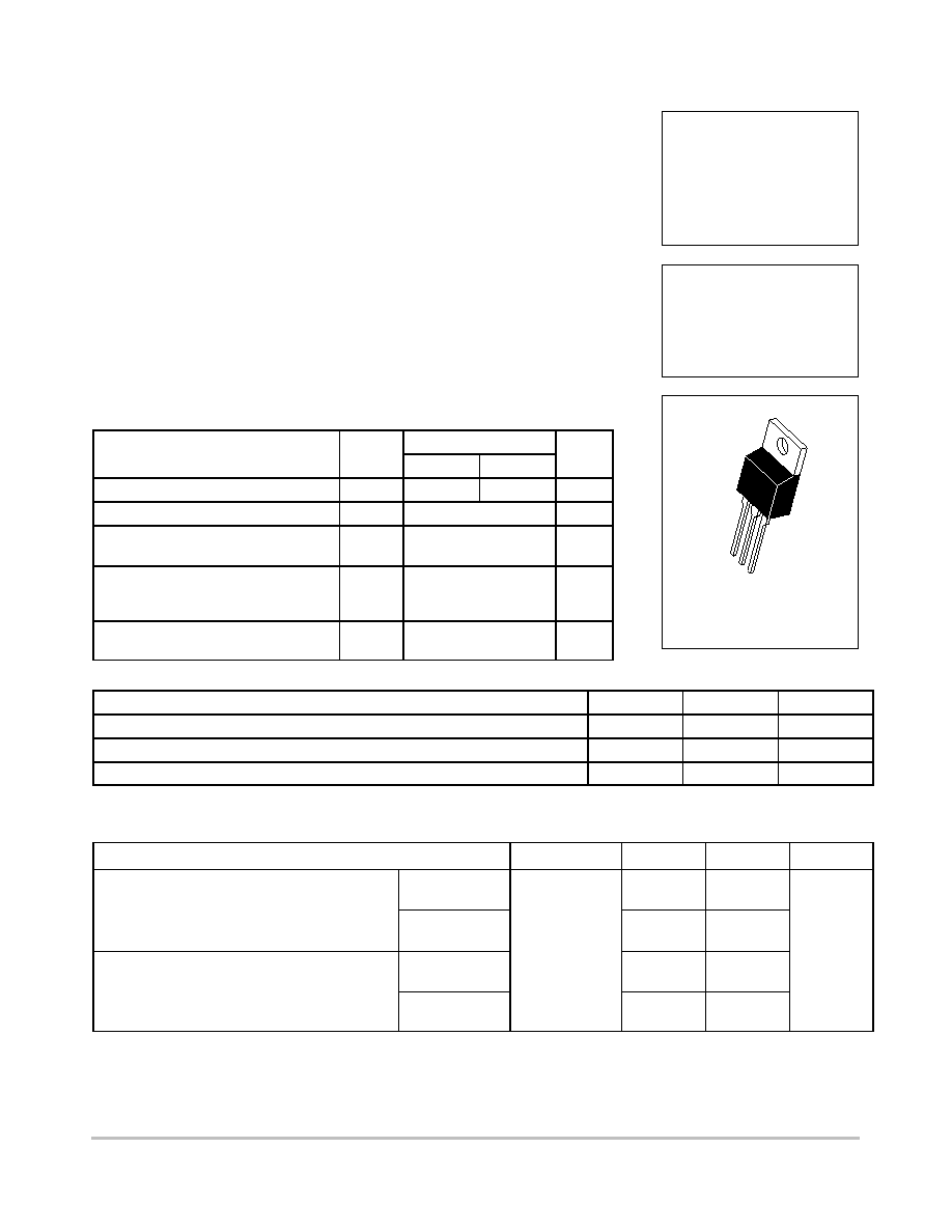
D44H Series
D45H Series
10 AMPERE
COMPLEMENTARY
SILICON
POWER TRANSISTORS
60, 80 VOLTS
*ON Semiconductor Preferred Device
*
NPN
*
PNP
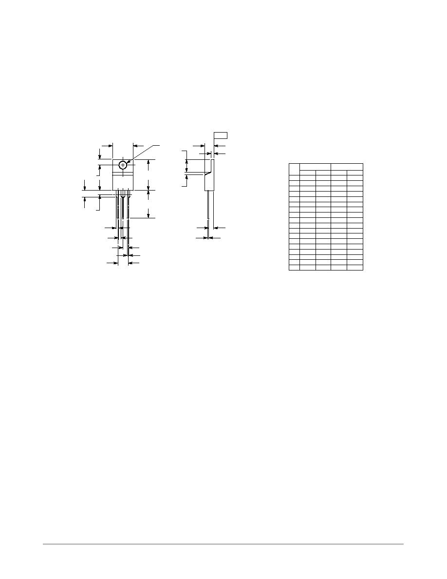
CASE 221A¡06
TO¡220AB

D44H Series D45H Series
http://onsemi.com
2
╬╬╬╬╬╬╬╬╬╬╬╬╬╬╬╬╬╬╬╬╬╬╬╬╬╬╬╬╬╬╬╬╬╬
╬╬╬╬╬╬╬╬╬╬╬╬╬╬╬╬╬╬╬╬╬╬╬╬╬╬╬╬╬╬╬╬╬╬
ELECTRICAL CHARACTERISTICS
(T
C
= 25
_
C unless otherwise noted)
╬╬╬╬╬╬╬╬╬╬╬╬╬╬╬╬╬╬╬╬
╬╬╬╬╬╬╬╬╬╬╬╬╬╬╬╬╬╬╬╬
Characteristic
╬╬╬╬
╬╬╬╬
Symbol
╬╬╬╬
╬╬╬╬
Min
╬╬╬╬
╬╬╬╬
Typ
╬╬╬╬
╬╬╬╬
Max
╬╬╬
╬╬╬
Unit
╬╬╬╬╬╬╬╬╬╬╬╬╬╬╬╬╬╬╬╬╬╬╬╬╬╬╬╬╬╬╬╬╬╬
╬╬╬╬╬╬╬╬╬╬╬╬╬╬╬╬╬╬╬╬╬╬╬╬╬╬╬╬╬╬╬╬╬╬
OFF CHARACTERISTICS
╬╬╬╬╬╬╬╬╬╬╬╬╬╬╬╬╬╬╬╬
╬
╬╬╬╬╬╬╬╬╬╬╬╬╬╬╬╬╬╬
╬
╬╬╬╬╬╬╬╬╬╬╬╬╬╬╬╬╬╬╬╬
Collector Cutoff Current
(V
CE
= Rated V
CEO
, V
BE
= 0)
╬╬╬╬
╬
╬╬
╬
╬╬╬╬
I
CES
╬╬╬╬
╬
╬╬
╬
╬╬╬╬
--
╬╬╬╬
╬
╬╬
╬
╬╬╬╬
--
╬╬╬╬
╬
╬╬
╬
╬╬╬╬
10
╬╬╬
╬
╬
╬
╬╬╬
╡
A
╬╬╬╬╬╬╬╬╬╬╬╬╬╬╬╬╬╬╬╬
╬
╬╬╬╬╬╬╬╬╬╬╬╬╬╬╬╬╬╬
╬
╬╬╬╬╬╬╬╬╬╬╬╬╬╬╬╬╬╬╬╬
Emitter Cutoff Current
(V
EB
= 5.0 Vdc)
╬╬╬╬
╬
╬╬
╬
╬╬╬╬
I
EBO
╬╬╬╬
╬
╬╬
╬
╬╬╬╬
--
╬╬╬╬
╬
╬╬
╬
╬╬╬╬
--
╬╬╬╬
╬
╬╬
╬
╬╬╬╬
100
╬╬╬
╬
╬
╬
╬╬╬
╡
A
╬╬╬╬╬╬╬╬╬╬╬╬╬╬╬╬╬╬╬╬╬╬╬╬╬╬╬╬╬╬╬╬╬╬
╬╬╬╬╬╬╬╬╬╬╬╬╬╬╬╬╬╬╬╬╬╬╬╬╬╬╬╬╬╬╬╬╬╬
ON CHARACTERISTICS
╬╬╬╬╬╬╬╬╬╬╬╬╬╬╬╬╬╬╬╬
╬
╬╬╬╬╬╬╬╬╬╬╬╬╬╬╬╬╬╬
╬
╬
╬╬╬╬╬╬╬╬╬╬╬╬╬╬╬╬╬╬
╬
╬╬╬╬╬╬╬╬╬╬╬╬╬╬╬╬╬╬╬╬
Collector¡Emitter Saturation Voltage
(I
C
= 8.0 Adc, I
B
= 0.4 Adc)
D44H/D45H8,11
(I
C
= 8.0 Adc, I
B
= 0.8 Adc)
D44H/D45H10
╬╬╬╬
╬
╬╬
╬
╬
╬╬
╬
╬╬╬╬
V
CE(sat)
╬╬╬╬
╬
╬╬
╬
╬
╬╬
╬
╬╬╬╬
--
--
╬╬╬╬
╬
╬╬
╬
╬
╬╬
╬
╬╬╬╬
--
--
╬╬╬╬
╬
╬╬
╬
╬
╬╬
╬
╬╬╬╬
1.0
1.0
╬╬╬
╬
╬
╬
╬
╬
╬
╬╬╬
Vdc
╬╬╬╬╬╬╬╬╬╬╬╬╬╬╬╬╬╬╬╬
╬╬╬╬╬╬╬╬╬╬╬╬╬╬╬╬╬╬╬╬
Base¡Emitter Saturation Voltage
(I
C
= 8.0 Adc, I
B
= 0.8 Adc)
╬╬╬╬
╬╬╬╬
V
BE(sat)
╬╬╬╬
╬╬╬╬
--
╬╬╬╬
╬╬╬╬
--
╬╬╬╬
╬╬╬╬
1.5
╬╬╬
╬╬╬
Vdc
╬╬╬╬╬╬╬╬╬╬╬╬╬╬╬╬╬╬╬╬╬╬╬╬╬╬╬╬╬╬╬╬╬╬
╬╬╬╬╬╬╬╬╬╬╬╬╬╬╬╬╬╬╬╬╬╬╬╬╬╬╬╬╬╬╬╬╬╬
DYNAMIC CHARACTERISTICS
╬╬╬╬╬╬╬╬╬╬╬╬╬╬╬╬╬╬╬╬
╬
╬╬╬╬╬╬╬╬╬╬╬╬╬╬╬╬╬╬
╬
╬
╬╬╬╬╬╬╬╬╬╬╬╬╬╬╬╬╬╬
╬
╬╬╬╬╬╬╬╬╬╬╬╬╬╬╬╬╬╬╬╬
Collector Capacitance
(V
CB
= 10 Vdc, f
test
= 1.0 MHz)
D44H Series
D45H Series
╬╬╬╬
╬
╬╬
╬
╬
╬╬
╬
╬╬╬╬
C
cb
╬╬╬╬
╬
╬╬
╬
╬
╬╬
╬
╬╬╬╬
--
--
╬╬╬╬
╬
╬╬
╬
╬
╬╬
╬
╬╬╬╬
130
230
╬╬╬╬
╬
╬╬
╬
╬
╬╬
╬
╬╬╬╬
--
--
╬╬╬
╬
╬
╬
╬
╬
╬
╬╬╬
pF
╬╬╬╬╬╬╬╬╬╬╬╬╬╬╬╬╬╬╬╬
╬
╬╬╬╬╬╬╬╬╬╬╬╬╬╬╬╬╬╬
╬
╬╬╬╬╬╬╬╬╬╬╬╬╬╬╬╬╬╬╬╬
Gain Bandwidth Product
(I
C
= 0.5 Adc, V
CE
= 10 Vdc, f = 20 MHz)
D44H Series
D45H Series
╬╬╬╬
╬
╬╬
╬
╬╬╬╬
f
T
╬╬╬╬
╬
╬╬
╬
╬╬╬╬
--
--
╬╬╬╬
╬
╬╬
╬
╬╬╬╬
50
40
╬╬╬╬
╬
╬╬
╬
╬╬╬╬
--
--
╬╬╬
╬
╬
╬
╬╬╬
MHz
╬╬╬╬╬╬╬╬╬╬╬╬╬╬╬╬╬╬╬╬╬╬╬╬╬╬╬╬╬╬╬╬╬╬
╬
╬╬╬╬╬╬╬╬╬╬╬╬╬╬╬╬╬╬╬╬╬╬╬╬╬╬╬╬╬╬╬╬
╬
╬╬╬╬╬╬╬╬╬╬╬╬╬╬╬╬╬╬╬╬╬╬╬╬╬╬╬╬╬╬╬╬╬╬
SWITCHING TIMES
╬╬╬╬╬╬╬╬╬╬╬╬╬╬╬╬╬╬╬╬
╬
╬╬╬╬╬╬╬╬╬╬╬╬╬╬╬╬╬╬
╬
╬╬╬╬╬╬╬╬╬╬╬╬╬╬╬╬╬╬╬╬
Delay and Rise Times
(I
C
= 5.0 Adc, I
B1
= 0.5 Adc)
D44H Series
D45H Series
╬╬╬╬
╬
╬╬
╬
╬╬╬╬
t
d
+ t
r
╬╬╬╬
╬
╬╬
╬
╬╬╬╬
--
--
╬╬╬╬
╬
╬╬
╬
╬╬╬╬
300
135
╬╬╬╬
╬
╬╬
╬
╬╬╬╬
--
--
╬╬╬
╬
╬
╬
╬╬╬
ns
╬╬╬╬╬╬╬╬╬╬╬╬╬╬╬╬╬╬╬╬
╬
╬╬╬╬╬╬╬╬╬╬╬╬╬╬╬╬╬╬
╬
╬
╬╬╬╬╬╬╬╬╬╬╬╬╬╬╬╬╬╬
╬
╬╬╬╬╬╬╬╬╬╬╬╬╬╬╬╬╬╬╬╬
Storage Time
(I
C
= 5.0 Adc, I
B1
= I
B2
= 0.5 Adc)
D44H Series
D45H Series
╬╬╬╬
╬
╬╬
╬
╬
╬╬
╬
╬╬╬╬
t
s
╬╬╬╬
╬
╬╬
╬
╬
╬╬
╬
╬╬╬╬
--
--
╬╬╬╬
╬
╬╬
╬
╬
╬╬
╬
╬╬╬╬
500
500
╬╬╬╬
╬
╬╬
╬
╬
╬╬
╬
╬╬╬╬
--
--
╬╬╬
╬
╬
╬
╬
╬
╬
╬╬╬
ns
╬╬╬╬╬╬╬╬╬╬╬╬╬╬╬╬╬╬╬╬
╬
╬╬╬╬╬╬╬╬╬╬╬╬╬╬╬╬╬╬
╬
╬╬╬╬╬╬╬╬╬╬╬╬╬╬╬╬╬╬╬╬
Fall Time
(I
C
= 5.0 Adc, I
B1
= 102 = 0.5 Adc)
D44H Series
D45H Series
╬╬╬╬
╬
╬╬
╬
╬╬╬╬
t
f
╬╬╬╬
╬
╬╬
╬
╬╬╬╬
--
--
╬╬╬╬
╬
╬╬
╬
╬╬╬╬
140
100
╬╬╬╬
╬
╬╬
╬
╬╬╬╬
--
--
╬╬╬
╬
╬
╬
╬╬╬
ns
100
1.0
V
CE
, COLLECTOR-EMITTER VOLTAGE (VOLTS)
5.0
10
T
C
70
░
C
DUTY CYCLE
50%
I C
, COLLECT
OR CURRENT
(AMPS)
2.0 3.0
20 30
50
100
1.0
7.0
D44H/45H8
D44H/45H10,11
Figure 1. Maximum Rated Forward Bias
Safe Operating Area
70
1.0
╡
s
dc
0.1
0.2
0.3
0.5
2.0
3.0
5.0
10
20
30
50
10
╡
s
100
╡
s
1.0 ms

D44H Series D45H Series
http://onsemi.com
4
ON Semiconductor and are trademarks of Semiconductor Components Industries, LLC (SCILLC). SCILLC reserves the right to make changes
without further notice to any products herein. SCILLC makes no warranty, representation or guarantee regarding the suitability of its products for any particular
purpose, nor does SCILLC assume any liability arising out of the application or use of any product or circuit, and specifically disclaims any and all liability,
including without limitation special, consequential or incidental damages. "Typical" parameters which may be provided in SCILLC data sheets and/or
specifications can and do vary in different applications and actual performance may vary over time. All operating parameters, including "Typicals" must be
validated for each customer application by customer's technical experts. SCILLC does not convey any license under its patent rights nor the rights of others.
SCILLC products are not designed, intended, or authorized for use as components in systems intended for surgical implant into the body, or other applications
intended to support or sustain life, or for any other application in which the failure of the SCILLC product could create a situation where personal injury or
death may occur. Should Buyer purchase or use SCILLC products for any such unintended or unauthorized application, Buyer shall indemnify and hold
SCILLC and its officers, employees, subsidiaries, affiliates, and distributors harmless against all claims, costs, damages, and expenses, and reasonable
attorney fees arising out of, directly or indirectly, any claim of personal injury or death associated with such unintended or unauthorized use, even if such claim
alleges that SCILLC was negligent regarding the design or manufacture of the part. SCILLC is an Equal Opportunity/Affirmative Action Employer.
PUBLICATION ORDERING INFORMATION
CENTRAL/SOUTH AMERICA:
Spanish Phone: 303¡308¡7143 (Mon¡Fri 8:00am to 5:00pm MST)
Email: ONlit¡spanish@hibbertco.com
Toll¡Free from Mexico: Dial 01¡800¡288¡2872 for Access ¡
then Dial 866¡297¡9322
ASIA/PACIFIC: LDC for ON Semiconductor ¡ Asia Support
Phone: 303¡675¡2121 (Tue¡Fri 9:00am to 1:00pm, Hong Kong Time)
Toll Free from Hong Kong & Singapore:
001¡800¡4422¡3781
Email: ONlit¡asia@hibbertco.com
JAPAN: ON Semiconductor, Japan Customer Focus Center
4¡32¡1 Nishi¡Gotanda, Shinagawa¡ku, Tokyo, Japan 141¡0031
Phone: 81¡3¡5740¡2700
Email: r14525@onsemi.com
ON Semiconductor Website: http://onsemi.com
For additional information, please contact your local
Sales Representative.
D44H/D
NORTH AMERICA Literature Fulfillment:
Literature Distribution Center for ON Semiconductor
P.O. Box 5163, Denver, Colorado 80217 USA
Phone: 303¡675¡2175 or 800¡344¡3860 Toll Free USA/Canada
Fax: 303¡675¡2176 or 800¡344¡3867 Toll Free USA/Canada
Email: ONlit@hibbertco.com
Fax Response Line: 303¡675¡2167 or 800¡344¡3810 Toll Free USA/Canada
N. American Technical Support: 800¡282¡9855 Toll Free USA/Canada
EUROPE: LDC for ON Semiconductor ¡ European Support
German Phone: (+1) 303¡308¡7140 (Mon¡Fri 2:30pm to 7:00pm CET)
Email: ONlit¡german@hibbertco.com
French Phone: (+1) 303¡308¡7141 (Mon¡Fri 2:00pm to 7:00pm CET)
Email: ONlit¡french@hibbertco.com
English Phone: (+1) 303¡308¡7142 (Mon¡Fri 12:00pm to 5:00pm GMT)
Email: ONlit@hibbertco.com
EUROPEAN TOLL¡FREE ACCESS*: 00¡800¡4422¡3781
*Available from Germany, France, Italy, UK, Ireland