©
Semiconductor Components Industries, LLC, 2001
November, 2001 ≠ Rev. 3
1
Publication Order Number:
DTC114E/D
DTC114E Series
Preferred Devices
Bias Resistor Transistor
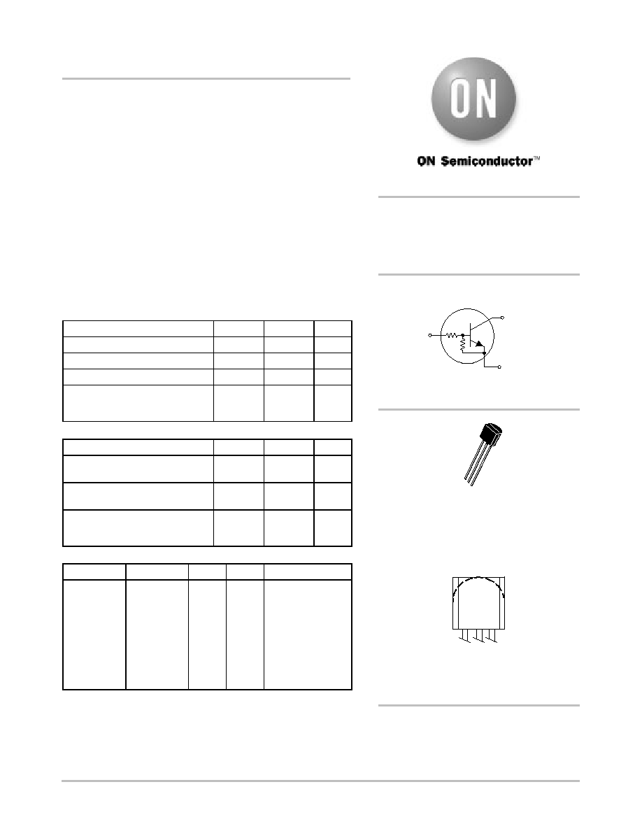
NPN Silicon Surface Mount Transistor
with Monolithic Bias Resistor Network
This new series of digital transistors is designed to replace a single
device and its external resistor bias network. The BRT (Bias Resistor
Transistor) contains a single transistor with a monolithic bias network
consisting of two resistors; a series base resistor and a base≠emitter
resistor. The BRT eliminates these individual components by
integrating them into a single device. The use of a BRT can reduce
both system cost and board space. The device is housed in the TO≠92
package which is designed for through hole applications.
MAXIMUM RATINGS
(TA = 25
∞
C unless otherwise noted)
Rating
Symbol
Value
Unit
Collector-Base Voltage
VCBO
50
Vdc
Collector-Emitter Voltage
VCEO
50
Vdc
Collector Current
IC
100
mAdc
Total Power Dissipation
@ TA = 25
∞
C (Note 1.)
Derate above 25
∞
C
PD
350
2.81
mW
mW/
∞
C
THERMAL CHARACTERISTICS
Characteristic
Symbol
Value
Unit
Thermal Resistance, Junction to
Ambient (surface mounted)
R
JA
357
∞
C/W
Operating and Storage
Temperature Range
TJ, Tstg
≠55 to
+150
∞
C
Maximum Temperature for
Soldering Purposes,
Time in Solder Bath
TL
260
10
∞
C
Sec
DEVICE MARKING AND RESISTOR VALUES
Device
Marking
R1 (K)
R2 (K)
Shipping
DTC114E
DTC124E
DTC144E
DTC114Y
DTC114T
DTC143T
DTD113E
DTC123E
DTC143E
DTC143Z
DTC114E
DTC124E
DTC144E
DTC114Y
DTC114T
DTC143T
DTD113E
DTC123E
DTC143E
DTC143Z
10
22
47
10
10
4.7
1.0
2.2
4.7
4.7
10
22
47
47
1.0
2.2
4.7
47
5000/Box
1. Device mounted on a FR≠4 glass epoxy printed circuit board using the
minimum recommended footprint.
http://onsemi.com
CASE 29
TO≠92 (TO≠226)
STYLE 1
Preferred devices are recommended choices for future use
and best overall value.
NPN SILICON
BIAS RESISTOR
TRANSISTOR
1
2
3
PIN 3
COLLECTOR
(OUTPUT)
PIN 1
EMITTER
(GROUND)
PIN 2
BASE
(INPUT)
R1
R2
DTC1
= Specific Device Code
xxx
= (See Table)
Y
= Year
WW
= Work Week
MARKING DIAGRAM
DTC1xxx
YWW

DTC114E Series
http://onsemi.com
2
ELECTRICAL CHARACTERISTICS
(TA = 25
∞
C unless otherwise noted)
Characteristic
Symbol
Min
Typ
Max
Unit
OFF CHARACTERISTICS
Collector≠Base Cutoff Current (VCB = 50 V, IE = 0)
ICBO
≠
≠
100
nAdc
Collector≠Emitter Cutoff Current (VCE = 50 V, IB = 0)
ICEO
≠
≠
500
nAdc
Emitter≠Base Cutoff Current
DTC114E
(VEB = 6.0 V, IC = 0)
DTC124E
DTC144E
DTC114Y
DTC114T
DTC143T
DTD113E
DTC123E
DTC143E
DTC143Z
IEBO
≠
≠
≠
≠
≠
≠
≠
≠
≠
≠
≠
≠
≠
≠
≠
≠
≠
≠
≠
≠
0.5
0.2
0.1
0.2
0.9
1.9
4.3
2.3
1.5
0.18
mAdc
Collector≠Base Breakdown Voltage (IC = 10
µ
A, IE = 0)
V(BR)CBO
50
≠
≠
Vdc
Collector≠Emitter Breakdown Voltage (Note 2.)
(IC = 2.0 mA, IB = 0)
V(BR)CEO
50
≠
≠
Vdc
ON CHARACTERISTICS
(Note 2.)
DC Current Gain
DTC114E
(VCE = 10 V, IC = 5.0 mA)
DTC124E
DTC144E
DTC114Y
DTC114T
DTC143T
DTD113E
DTC123E
DTC143E
DTC143Z
hFE
35
60
80
80
160
160
3.0
8.0
15
80
60
100
140
140
350
350
5.0
15
30
200
≠
≠
≠
≠
≠
≠
≠
≠
≠
≠
Collector≠Emitter Saturation Voltage
(IC = 10 mA, IE = 0.3 mA) DTC144E/DTC114Y
(IC = 10 mA, IB = 0.3 mA)
DTD113E/DTC143E
(IC = 10 mA, IB = 5 mA) DTC123E
(IC = 10 mA, IB = 1 mA) DTC114T/DTC143T/
(IC = 10 mA, IB = 1 mA)
DTC143Z/DTC124E
VCE(sat)
≠
≠
0.25
Vdc
Output Voltage (on)
(VCC = 5.0 V, VB = 2.5 V, RL = 1.0 k
)
DTC114E
DTC124E
DTC114Y
DTC114T
DTC143T
DTD113E
DTC123E
DTC143E
DTC143Z
(VCC = 5.0 V, VB = 3.5 V, RL = 1.0 k
)
DTC144E
VOL
≠
≠
≠
≠
≠
≠
≠
≠
≠
≠
≠
≠
≠
≠
≠
≠
≠
≠
≠
≠
0.2
0.2
0.2
0.2
0.2
0.2
0.2
0.2
0.2
0.2
Vdc
2. Pulse Test: Pulse Width < 300
µ
s, Duty Cycle < 2.0%

DTC114E Series
http://onsemi.com
3
ELECTRICAL CHARACTERISTICS
(TA = 25
∞
C unless otherwise noted) (Continued)
Characteristic
Symbol
Min
Typ
Max
Unit
Output Voltage (off)
(VCC = 5.0 V, VB = 0.5 V, RL = 1.0 k
)
DTC114E
DTC124E
DTC144E
DTC114Y
DTC123E
DTC143E
(VCC = 5.0 V, VB = 0.05 V, RL = 1.0 k
)
DTD113E
(VCC = 5.0 V, VB = 0.25 V, RL = 1.0 k
)
DTC114T
DTC143T
DTC143Z
VOH
4.9
≠
≠
Vdc
Input Resistor
DTC114E
DTC124E
DTC144E
DTC114Y
DTC114T
DTC143T
DTD113E
DTC123E
DTC143E
DTC143Z
R1
7.0
15.4
32.9
7.0
7.0
3.3
0.7
1.5
3.3
3.3
10
22
47
10
10
4.7
1.0
2.2
4.7
4.7
13
28.6
61.1
13
13
6.1
1.3
2.9
6.1
6.1
k
Resistor Ratio
DTC114E/DTC124E/DTC144E
DTC114Y
DTC114T/DTC143T
DTD113E/DTC123E/DTC143E
DTC143Z
R1/R2
0.8
0.17
≠
0.8
0.055
1.0
0.21
≠
1.0
0.1
1.2
0.25
≠
1.2
0.185
DTC114E Series
http://onsemi.com
4
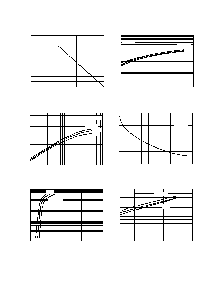
TYPICAL ELECTRICAL CHARACTERISTICS
DTC114E
10
0
20
30
IC, COLLECTOR CURRENT (mA)
10
1
0.1
V in
, INPUT
VOL
T
AGE (VOL
TS)
TA = -25
∞
C
75
∞
C
25
∞
C
40
50
1
0.1
0.01
0.001
0
20
40
60
80
IC, COLLECTOR CURRENT (mA)
V CE(sat)
, MAXIMUM COLLECT
OR VOL
T
AGE (VOL
TS)
1000
100
10
1
10
100
IC, COLLECTOR CURRENT (mA)
h FE
, DC CURRENT
GAIN (NORMALIZED)
TA = 75
∞
C
25
∞
C
-25
∞
C
TA = -25
∞
C
25
∞
C
IC/IB = 10
75
∞
C
25
∞
C
TA = -25
∞
C
100
10
1
0.1
0.01
0.001
0
1
2
3
4
Vin, INPUT VOLTAGE (VOLTS)
I C
, COLLECT
OR CURRENT
(mA)
5
6
7
8
9
10
50
0
10
20
30
40
4
3
1
2
0
VR, REVERSE BIAS VOLTAGE (VOLTS)
C ob
, CAP
ACIT
ANCE (pF)
75
∞
C
f = 1 MHz
lE = 0 V
TA = 25
∞
C
VO = 5 V
VCE = 10 V
VO = 0.2 V
Figure 1. Derating Curve
250
200
150
100
50
0
-50
0
50
100
150
TA, AMBIENT TEMPERATURE (
∞
C)
P D
, POWER DISSIP
A
TION (MILLIW
A
TTS)
R
JA = 625
∞
C/W
Figure 2. VCE(sat) versus IC
Figure 3. DC Current Gain
Figure 4. Output Capacitance
Figure 5. VCE(sat) versus IC
Figure 6. VCE(sat) versus IC
DTC114E Series
http://onsemi.com
5
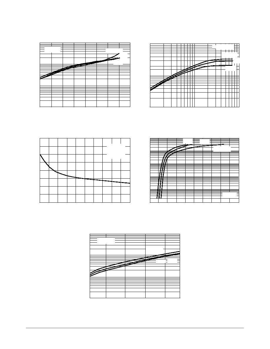
TYPICAL ELECTRICAL CHARACTERISTICS
DTC124E
Figure 7. VCE(sat) versus IC
Figure 8. DC Current Gain
Figure 9. Output Capacitance
Figure 10. Output Current versus Input Voltage
1000
10
IC, COLLECTOR CURRENT (mA)
h FE
, DC CURRENT
GAIN (NORMALIZED) 100
10
1
100
75
∞
C
25
∞
C
100
0
Vin, INPUT VOLTAGE (VOLTS)
I C
, COLLECT
OR CURRENT
(mA)
10
1
0.1
0.01
0.001
2
4
6
8
10
TA = -25
∞
C
0
IC, COLLECTOR CURRENT (mA)
100
V in
, INPUT
VOL
T
AGE (VOL
TS)
TA = -25
∞
C
75
∞
C
10
1
0.1
10
20
30
40
50
Figure 11. Input Voltage versus Output Current
0.001
V CE(sat)
, MAXIMUM COLLECT
OR VOL
T
AGE (VOL
T
S
TA = -25
∞
C
75
∞
C
25
∞
C
0.01
0.1
1
40
IC, COLLECTOR CURRENT (mA)
0
20
60
80
50
0
10
20
30
40
4
3
2
1
0
VR, REVERSE BIAS VOLTAGE (VOLTS)
C ob
, CAP
ACIT
ANCE (pF)
f = 1 MHz
lE = 0 V
TA = 25
∞
C
VO = 5 V
VO = 0.2 V
IC/IB = 10
25
∞
C
TA = 75
∞
C
-25
∞
C
VCE = 10 V
25
∞
C
-

DTC114E Series
http://onsemi.com
6
TYPICAL ELECTRICAL CHARACTERISTICS
DTC144E
Figure 12. VCE(sat) versus IC
0
2
4
6
8
10
100
10
1
0.1
0.01
0.001
I C
, COLLECT
OR CURRENT
(mA)
Vin, INPUT VOLTAGE (VOLTS)
TA = -25
∞
C
75
∞
C
25
∞
C
Figure 13. DC Current Gain
Figure 14. Output Capacitance
100
10
1
0.1
0
10
20
30
40
50
V in
, INPUT
VOL
T
AGE (VOL
TS)
IC, COLLECTOR CURRENT (mA)
Figure 15. Output Current versus Input Voltage
1000
10
IC, COLLECTOR CURRENT (mA)
h FE
, DC CURRENT
GAIN (NORMALIZED)
TA = 75
∞
C
25
∞
C
-25
∞
C
100
101
100
Figure 16. Input Voltage versus Output Current
0
20
40
60
80
10
1
0.1
0.01
IC, COLLECTOR CURRENT (mA)
TA = -25
∞
C
25
∞
C
75
∞
C
V CE(sat)
, MAXIMUM COLLECT
OR VOL
T
AGE (VOL
TS)
TA = -25
∞
C
25
∞
C
75
∞
C
50
0
10
20
30
40
1
0.8
0.6
0.4
0.2
0
VR, REVERSE BIAS VOLTAGE (VOLTS)
C ob
, CAP
ACIT
ANCE (pF)
f = 1 MHz
lE = 0 V
TA = 25
∞
C
VO = 5 V
VCE = 10 V
IC/IB = 10
VO = 0.2 V

DTC114E Series
http://onsemi.com
7
TYPICAL ELECTRICAL CHARACTERISTICS
DTC114Y
10
1
0.1
0
10
20
30
40
50
100
10
1
0
2
4
6
8
10
4
3.5
3
2.5
2
1.5
1
0.5
0
0
2
4
6
8 10 15 20 25 30 35 40 45 50
VR, REVERSE BIAS VOLTAGE (VOLTS)
V in
, INPUT
VOL
T
AGE (VOL
TS)
I C
, COLLECT
OR CURRENT
(mA)
h FE
, DC CURRENT
GAIN (NORMALIZED)
Figure 17. VCE(sat) versus IC
IC, COLLECTOR CURRENT (mA)
0
20
40
60
80
V CE(sat)
, MAXIMUM COLLECT
OR VOL
T
AGE (VOL
T
S
Figure 18. DC Current Gain
1
10
100
IC, COLLECTOR CURRENT (mA)
Figure 19. Output Capacitance
Figure 20. Output Current versus Input Voltage
Vin, INPUT VOLTAGE (VOLTS)
C ob
, CAP
ACIT
ANCE (pF)
Figure 21. Input Voltage versus Output Current
IC, COLLECTOR CURRENT (mA)
1
0.1
0.01
0.001
-25
∞
C
25
∞
C
TA = 75
∞
C
VCE = 10
300
250
200
150
100
50
0
2 4
6
8
15 20 40 50 60 70 80 90
f = 1 MHz
lE = 0 V
TA = 25
∞
C
TA = -25
∞
C
25
∞
C
75
∞
C
IC/IB = 10
75
∞
C
25
∞
C
TA = -25
∞
C
VO = 5 V
VO = 0.2 V
TA = -25
∞
C
25
∞
C
75
∞
C
DTC114E Series
http://onsemi.com
8
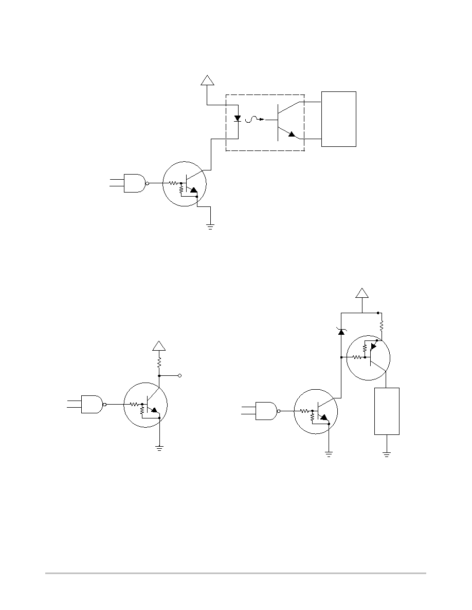
TYPICAL APPLICATIONS FOR NPN BRTs
LOAD
+12 V
Figure 22. Level Shifter: Connects 12 or 24 Volt Circuits to Logic
IN
OUT
VCC
ISOLATED
LOAD
FROM
µ
P OR
OTHER LOGIC
+12 V
Figure 23. Open Collector Inverter: Inverts
the Input Signal
Figure 24. Inexpensive, Unregulated Current Source
DTC114E Series
http://onsemi.com
9
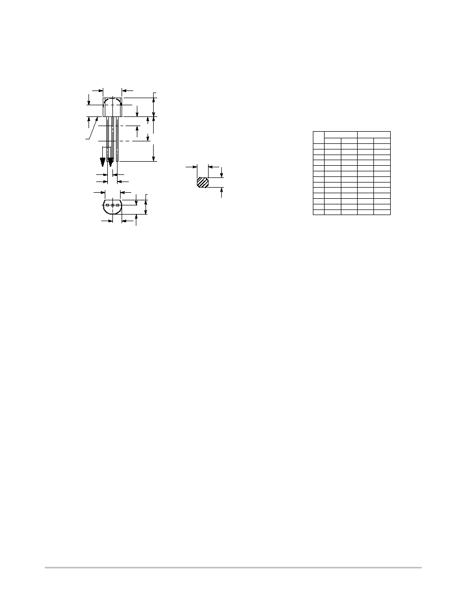
PACKAGE DIMENSIONS
TO≠92
TO≠226AA
CASE 29≠11
ISSUE AL
NOTES:
1. DIMENSIONING AND TOLERANCING PER ANSI
Y14.5M, 1982.
2. CONTROLLING DIMENSION: INCH.
3. CONTOUR OF PACKAGE BEYOND DIMENSION R
IS UNCONTROLLED.
4. LEAD DIMENSION IS UNCONTROLLED IN P AND
BEYOND DIMENSION K MINIMUM.
R
A
P
J
L
B
K
G
H
SECTION X≠X
C
V
D
N
N
X X
SEATING
PLANE
DIM
MIN
MAX
MIN
MAX
MILLIMETERS
INCHES
A
0.175
0.205
4.45
5.20
B
0.170
0.210
4.32
5.33
C
0.125
0.165
3.18
4.19
D
0.016
0.021
0.407
0.533
G
0.045
0.055
1.15
1.39
H
0.095
0.105
2.42
2.66
J
0.015
0.020
0.39
0.50
K
0.500
---
12.70
---
L
0.250
---
6.35
---
N
0.080
0.105
2.04
2.66
P
---
0.100
---
2.54
R
0.115
---
2.93
---
V
0.135
---
3.43
---
1
STYLE 1:
PIN 1. EMITTER
2. BASE
3. COLLECTOR

DTC114E Series
http://onsemi.com
10
Notes

DTC114E Series
http://onsemi.com
11
Notes

DTC114E Series
http://onsemi.com
12
PUBLICATION ORDERING INFORMATION
JAPAN: ON Semiconductor, Japan Customer Focus Center
4≠32≠1 Nishi≠Gotanda, Shinagawa≠ku, Tokyo, Japan 141≠0031
Phone: 81≠3≠5740≠2700
Email: r14525@onsemi.com
ON Semiconductor Website: http://onsemi.com
For additional information, please contact your local
Sales Representative.
Literature Fulfillment:
Literature Distribution Center for ON Semiconductor
P.O. Box 5163, Denver, Colorado 80217 USA
Phone: 303≠675≠2175 or 800≠344≠3860 Toll Free USA/Canada
Fax: 303≠675≠2176 or 800≠344≠3867 Toll Free USA/Canada
Email: ONlit@hibbertco.com
N. American Technical Support: 800≠282≠9855 Toll Free USA/Canada
ON Semiconductor and are trademarks of Semiconductor Components Industries, LLC (SCILLC). SCILLC reserves the right to make changes
without further notice to any products herein. SCILLC makes no warranty, representation or guarantee regarding the suitability of its products for any particular
purpose, nor does SCILLC assume any liability arising out of the application or use of any product or circuit, and specifically disclaims any and all liability,
including without limitation special, consequential or incidental damages. "Typical" parameters which may be provided in SCILLC data sheets and/or
specifications can and do vary in different applications and actual performance may vary over time. All operating parameters, including "Typicals" must be
validated for each customer application by customer's technical experts. SCILLC does not convey any license under its patent rights nor the rights of others.
SCILLC products are not designed, intended, or authorized for use as components in systems intended for surgical implant into the body, or other applications
intended to support or sustain life, or for any other application in which the failure of the SCILLC product could create a situation where personal injury or
death may occur. Should Buyer purchase or use SCILLC products for any such unintended or unauthorized application, Buyer shall indemnify and hold
SCILLC and its officers, employees, subsidiaries, affiliates, and distributors harmless against all claims, costs, damages, and expenses, and reasonable
attorney fees arising out of, directly or indirectly, any claim of personal injury or death associated with such unintended or unauthorized use, even if such claim
alleges that SCILLC was negligent regarding the design or manufacture of the part. SCILLC is an Equal Opportunity/Affirmative Action Employer.
DTC114E/D