©
Semiconductor Components Industries, LLC, 2004
August, 2004 - Rev. 1
1
Publication Order Number:
ECLSOIC8EVB/D
ECLSOIC8EVB
Evaluation Board Manual
for High Frequency SOIC 8
INTRODUCTION
ON Semiconductor has developed an evaluation board for
the devices in 8-lead SOIC package. These evaluation
boards are offered as a convenience for the customers
interested in performing their own engineering assessment
on the general performance of the 8-lead SOIC device
samples. The board provides a high bandwidth 50
W
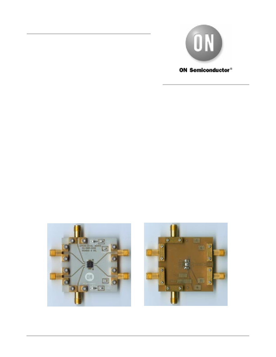
controlled impedance environment. The pictures in Figure 1
show the top and bottom view of the evaluation board, which
can be configured in several different ways, depending on
device under test (See Table 1. Configuration List).
This evaluation board manual contains:
·
Information on 8-lead SOIC Evaluation Board
·
Assembly Instructions
·
Appropriate Lab Setup
·
Bill of Materials
This manual should be used in conjunction with the device
data sheet, which contains full technical details on the device
specifications and operation.
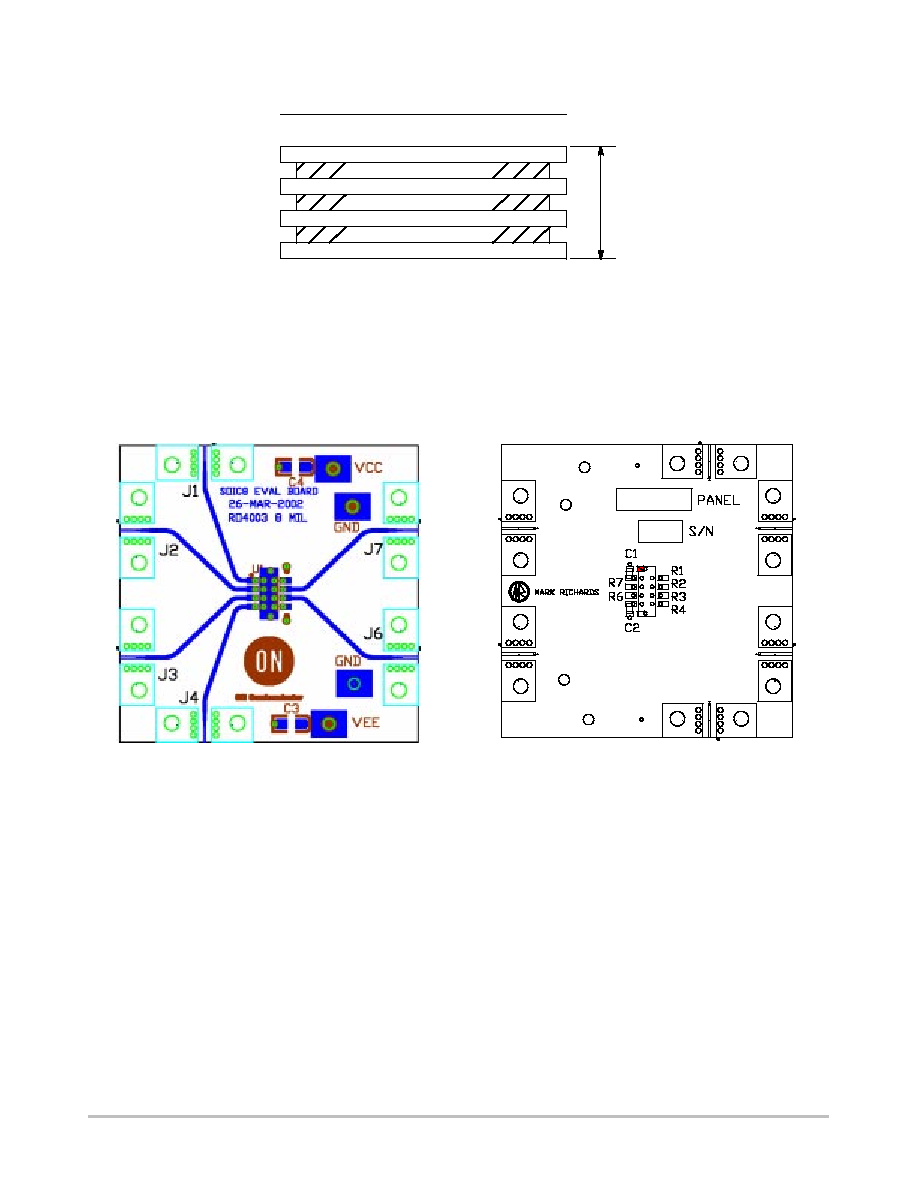
Board Lay-Up
The 8-lead SOIC evaluation board is implemented in four
layers with split (dual) power supplies (Figure 2.
Evaluation Board Lay-up). For standard ECL lab setup and
test, a split (dual) power supply is essential to enable the
50
W internal impedance in the oscilloscope as a termination
for ECL devices. The first layer or primary trace layer is
0.008
thick Rogers RO4003 material, which is designed to
have equal electrical length on all signal traces from the
device under the test (DUT) to the sense output. The second
layer is the 1.0 oz copper ground plane and a portion of the
plane is the V
EE
power plane. The FR4 dielectric material is
placed between second and third layer and between third and
fourth layer. The third layer is also 1.0 oz copper ground
plane and a portion of this layer is V
CC
power plane. The
fourth layer is the secondary trace layer.
Figure 1. Top and Bottom View of the 8-lead SOIC Evaluation Board
EVALUATION BOARD MANUAL
http://onsemi.com
ECLSOIC8EVB
http://onsemi.com
2
Figure 2. Evaluation Board Lay-up
LAY-UP DETAIL
4 LAYER
LAYER 1 (TOP SIDE)
ROGERS 4003 0.008 in
LAYER 2 (GROUND AND VEE PLANE P1) 1 OZ
FR-4 0.020 in
LAYER 3 (GROUND AND VCC PLANE P2) 1 OZ
FR-4 0.025 in
LAYER 4 (BOTTOM SIDE)
SILKSCREEN (TOP SIDE)
0.062
$
0.007
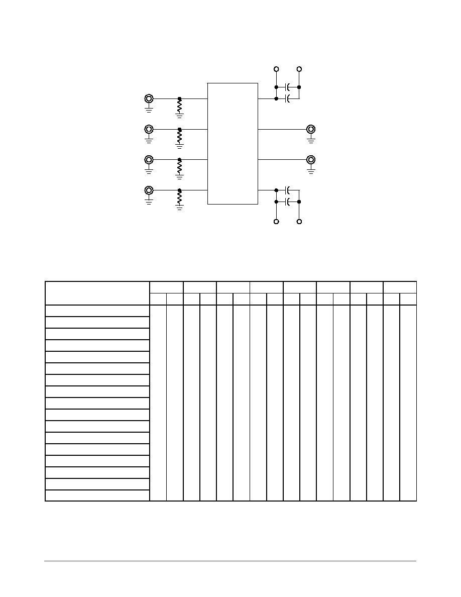
Board Layout
The 8-lead SOIC evaluation board was designed to be
versatile and accommodate several different configurations.
The input, output, and power pin layout of the evaluation
board is shown in Figure 3. The evaluation board has at least
eleven possible configurable options. Table 1. list the
devices and the relevant configuration that utilizes this PCB
board. List of components and simple schematics are located
in Figures 4 through 14. Place SMA connectors on J1
through J7, 50
W chip resistors on R1 through R7, and chip
capacitors C1 through C4 according to configuration
figures. (C1 and C2 are 0.01
mF and C3 and C4 are 0.1 mF).
Figure 3. Evaluation Board Layout
Top View
Bottom View
ECLSOIC8EVB
http://onsemi.com
4
Evaluation Board Assembly Instructions
The 8-lead SOIC evaluation board is designed for
characterizing devices in a 50
W laboratory environment
using high bandwidth equipment. Each signal trace on the
board has a via, which has an option of termination resistor
or bypassing capacitor depending on the input/output
configuration (see Table 1. Configuration List). Table 17
contains the Bill of Materials for this evaluation board.
Solder the Device on the Evaluation Board
The soldering can be accomplished by hand soldering or
soldering re-flow techniques. Make sure pin 1 of the device
is located next the white dotted mark U1 and all the pins are
aligned to the footprint pads. Solder the 8-lead SOIC device
to the evaluation board.
Connecting Power and Ground Planes
For standard ECL lab setup and test, a split (dual) power
supply is required enabling the 50
W internal impedance in
the oscilloscope to be used as a termination of the ECL
signals (V
TT
= V
CC
2.0 V, in split power supply setup, V
TT
is the system ground, V
CC
is 2.0 V, and V
EE
is 3.0 V or
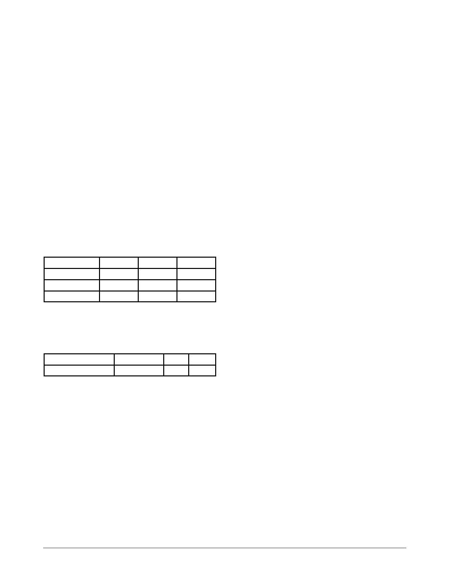
1.3 V; see Table 2: Power Supply Levels).
Table 2. Power Supply Levels
Power Supply
V
CC
V
EE
GND
5.0 V
2.0 V
-3.0 V
0.0 V
3.3 V
2.0 V
-1.3 V
0.0 V
2.5 V
2.0 V
-0.5 V
0.0 V
The power supply for voltage level translating device need
slight modification as indicated in Table 3. Power Supply
Levels for Translators.
Table 3. Power Supply Levels for Translators
V
CC
V
EE
GND
PECL Translators
3.3 V / 5.0 V
0.0 V
0.0 V
On the top side of the evaluation board solder the four
surface mount test point clips to the pads labeled V
CC
, V
EE
,
and GND. The V
CC
clip connects directly to pin 8 of the
device. The V
EE
clip connects directly to pin 5 of the device.
There are two GND clip footprints which can be connected
to the ground plane of the evaluation board depending on the
setup configuration.
It is recommended to solder 0.01
mF capacitors to C1 and
C2 to reduce the unwanted noise from the power supplies.
C3 and C4 pads are provided for 0.1
mF capacitor to further
diminish the noise from the power supplies. Adding
capacitors can improve edge rates, reduce overshoot and
undershoot.
Termination
All ECL outputs need to be terminated to V
TT
(V
TT
= V
CC
2.0 V = GND) via a 50
W resistor in a split power supply
lab set-up. 0603 chip resistor pads are provided on the
bottom side of the evaluation board to terminate the ECL
driver (More information on termination is provided in
AN8020). Solder the chip resistors to the bottom side of the
board on the appropriate input of the device pins labeled R1,
R2, R3, R4, R6, and R7, depending on the specific device.
Installing the SMA Connectors
Each configuration indicates the number of SMA
connectors needed to populate an evaluation board for a
given configuration. Each input and output requires one
SMA connector. Attach all the required SMA connectors
onto the board and solder the connectors to the board. Please
note that alignment of the signal connector pin of the SMA
can influence the lab results. The reflection and launch of the
signals are largely influenced by imperfect alignment and
soldering of the SMA connector.
Validating the Assembled Board
After assembling the evaluation board, it is recommended
to perform continuity checks on all soldered areas before
commencing with the evaluation process. Time Domain
Reflectometry (TDR) is another highly recommended
validation test.