 | –≠–ª–µ–∫—Ç—Ä–æ–Ω–Ω—ã–π –∫–æ–º–ø–æ–Ω–µ–Ω—Ç: J111RL1 | –°–∫–∞—á–∞—Ç—å:  PDF PDF  ZIP ZIP |
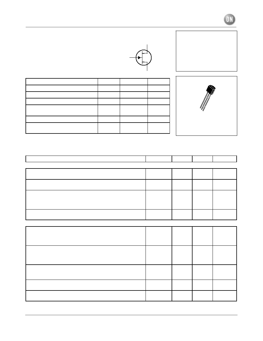
JFET Chopper Transistors
N≠Channel -- Depletion
MAXIMUM RATINGS
Rating
Symbol
Value
Unit
Drain≠Gate Voltage
VDG
≠35
Vdc
Gate≠Source Voltage
VGS
≠35
Vdc
Gate Current
IG
50
mAdc
Total Device Dissipation @ TA = 25
∞
C
Derate above 25
∞
C
PD
350
2.8
mW
mW/
∞
C
Lead Temperature
TL
300
∞
C
Operating and Storage Junction
Temperature Range
TJ, Tstg
≠65 to +150
∞
C
ELECTRICAL CHARACTERISTICS
(TA = 25
∞
C unless otherwise noted)
Characteristic
Symbol
Min
Max
Unit
OFF CHARACTERISTICS
Gate≠Source Breakdown Voltage
(IG = ≠1.0
µ
Adc)
V(BR)GSS
35
--
Vdc
Gate Reverse Current
(VGS = ≠15 Vdc)
IGSS
--
≠1.0
nAdc
Gate Source Cutoff Voltage
(VDS = 5.0 Vdc, ID = 1.0
µ
Adc)
J111
J112
J113
VGS(off)
≠3.0
≠1.0
≠0.5
≠10
≠5.0
≠3.0
Vdc
Drain≠Cutoff Current
(VDS = 5.0 Vdc, VGS = ≠10 Vdc)
ID(off)
--
1.0
nAdc
ON CHARACTERISTICS
Zero≠Gate≠Voltage Drain Current(1)
(VDS = 15 Vdc)
J111
J112
J113
IDSS
20
5.0
2.0
--
--
--
mAdc
Static Drain≠Source On Resistance
(VDS = 0.1 Vdc)
J111
J112
J113
rDS(on)
--
--
--
30
50
100
Drain Gate and Source Gate On≠Capacitance
(VDS = VGS = 0, f = 1.0 MHz)
Cdg(on)
+
Csg(on)
--
28
pF
Drain Gate Off≠Capacitance
(VGS = ≠10 Vdc, f = 1.0 MHz)
Cdg(off)
--
5.0
pF
Source Gate Off≠Capacitance
(VGS = ≠10 Vdc, f = 1.0 MHz)
Csg(off)
--
5.0
pF
1. Pulse Width = 300
µ
s, Duty Cycle = 3.0%.
ON Semiconductort
©
Semiconductor Components Industries, LLC, 2001
June, 2001 ≠ Rev. 1
1
Publication Order Number:
J111/D
J111
J112
J113
CASE 29≠11, STYLE 5
TO≠92 (TO≠226AA)
1
2
3
1 DRAIN
2 SOURCE
3
GATE

J111 J112 J113
http://onsemi.com
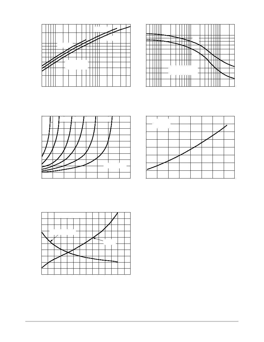
2
t f
, F
ALL
TIME (ns)
t r
, RISE
TIME (ns)
t d(on)
,
TURN-ON DELA
Y
TIME (ns)
1000
1.0
2.0
5.0
10
20
50
100
200
500
0.5 0.7 1.0
2.0 3.0
5.0 7.0 10
20 30
50
ID, DRAIN CURRENT (mA)
Figure 1. Turn≠On Delay Time
RK = 0
TJ = 25
∞
C
J111
J112
J113
VGS(off) = 12 V
= 7.0 V
= 5.0 V
RK = RD
1000
1.0
2.0
5.0
10
20
50
100
200
500
0.5 0.7 1.0
2.0 3.0
5.0 7.0 10
20 30
50
ID, DRAIN CURRENT (mA)
Figure 2. Rise Time
RK = RD
RK = 0
TJ = 25
∞
C
J111
J112
J113
VGS(off) = 12 V
= 7.0 V
= 5.0 V
1000
1.0
2.0
5.0
10
20
50
100
200
500
0.5 0.7 1.0
2.0 3.0
5.0 7.0 10
20 30
50
ID, DRAIN CURRENT (mA)
Figure 3. Turn≠Off Delay Time
RK = RD
RK = 0
TJ = 25
∞
C
J111
J112
J113
VGS(off) = 12 V
= 7.0 V
= 5.0 V
t d(of
f),
TURN-OFF DELA
Y
TIME (ns)
1000
1.0
2.0
5.0
10
20
50
100
200
500
0.5 0.7 1.0
2.0 3.0
5.0 7.0 10
20 30
50
ID, DRAIN CURRENT (mA)
Figure 4. Fall Time
RK = RD
RK = 0
TJ = 25
∞
C
J111
J112
J113
VGS(off) = 12 V
= 7.0 V
= 5.0 V
TYPICAL SWITCHING CHARACTERISTICS
NOTE 1
The switching characteristics shown above were measured using a test cir-
cuit similar to Figure 5. At the beginning of the switching interval, the gate
voltage is at Gate Supply Voltage (≠VGG). The Drain≠Source Voltage
(VDS) is slightly lower than Drain Supply Voltage (VDD) due to the voltage
divider. Thus Reverse Transfer Capacitance (Crss) or Gate≠Drain Capaci-
tance (Cgd) is charged to VGG + VDS.
During the turn≠on interval, Gate≠Source Capacitance (Cgs) discharges
through the series combination of RGen and RK. Cgd must discharge to
VDS(on) through RG and RK in series with the parallel combination of ef-
fective load impedance (R
D) and Drain≠Source Resistance (rds). During
the turn≠off, this charge flow is reversed.
Predicting turn≠on time is somewhat difficult as the channel resistance
rds is a function of the gate≠source voltage. While Cgs discharges, VGS ap-
proaches zero and rds decreases. Since Cgd discharges through rds, turn≠on
time is non≠linear. During turn≠off, the situation is reversed with rds in-
creasing as Cgd charges.
The above switching curves show two impedance conditions; 1) RK is
equal to RD, which simulates the switching behavior of cascaded stages
where the driving source impedance is normally the load impedance of the
previous stage, and 2) RK = 0 (low impedance) the driving source imped-
ance is that of the generator.
RGEN
50
VGEN
INPUT RK
50
RGG
VGG
50
OUTPUT
RD
+VDD
RT
SET VDS(off) = 10 V
INPUT PULSE
tr
tf
PULSE WIDTH
DUTY CYCLE
0.25 ns
0.5 ns
= 2.0
µ
s
2.0%
RGG & RK
RD +
RD(RT ) 50)
RD ) RT ) 50
Figure 5. Switching Time Test Circuit
J111 J112 J113
http://onsemi.com
3
r ds(on)
, DRAIN-SOURCE ON-ST
A
T
E
RESIST
ANCE (OHMS)
NOTE 2
The Zero≠Gate≠Voltage Drain Current (IDSS), is the principle de-
terminant of other J-FET characteristics. Figure 10 shows the
relationship of Gate≠Source Off Voltage (VGS(off) and Drain≠
Source On Resistance (rds(on)) to IDSS. Most of the devices will
be within
±
10% of the values shown in Figure 10. This data will
be useful in predicting the characteristic variations for a given
part number.
For example:
Unknown
rds(on) and VGS range for an J112
The electrical characteristics table indicates that an J112 has
an IDSS range of 25 to 75 mA. Figure 10, shows rds(on) = 52 Ohms
for IDSS = 25 mA and 30 Ohms for IDSS = 75 mA. The corre-
sponding VGS values are 2.2 volts and 4.8 volts.
y fs
, FOR
W
ARD
TRANSFER
ADMITT
ANCE (mmho
s
C, CAP
ACIT
ANCE (pF)
r ds(on)
, DRAIN-SOURCE ON-ST
A
T
E
RESIST
ANCE (OHMS)
r ds(on)
, DRAIN-SOURCE ON-ST
A
T
E
RESIST
ANCE (NORMALIZED)
2.0
3.0
5.0
7.0
10
20
0.5 0.7 1.0
2.0 3.0
5.0 7.0 10
20 30
50
ID, DRAIN CURRENT (mA)
Figure 6. Typical Forward Transfer Admittance
1.0
1.5
2.0
3.0
5.0
7.0
10
15
0.03 0.05 0.1
0.3 0.5
1.0
3.0 5.0
10
30
VR, REVERSE VOLTAGE (VOLTS)
Figure 7. Typical Capacitance
200
160
120
80
40
0
0
1.0
2.0
3.0
4.0
5.0
6.0
7.0
8.0
VGS, GATE-SOURCE VOLTAGE (VOLTS)
Figure 8. Effect of Gate≠Source Voltage
On Drain≠Source Resistance
2.0
1.8
1.6
1.4
1.2
1.0
0.8
0.6
0.4
-70
-40
-10
20
50
80
110
140
170
Tchannel, CHANNEL TEMPERATURE (
∞
C)
Figure 9. Effect of Temperature On
Drain≠Source On≠State Resistance
J113
J112
J111
Tchannel = 25
∞
C
VDS = 15 V
Cgs
Cgd
Tchannel = 25
∞
C
(Cds IS NEGLIGIBLE)
IDSS
= 10
mA
25
mA
50 mA 75 mA 100 mA
125 mA
Tchannel = 25
∞
C
ID = 1.0 mA
VGS = 0
10
IDSS, ZERO-GATE-VOLTAGE DRAIN CURRENT (mA)
Figure 10. Effect of IDSS On Drain≠Source
Resistance and Gate≠Source Voltage
20 30 40 50 60 70 80 90 100 110 120 130 140 150
10
9.0
8.0
7.0
6.0
5.0
4.0
3.0
2.0
1.0
0
100
90
80
70
60
50
40
30
20
10
0
V GS
, GA
TE-SOURCE VOL
T
AGE (VOL
TS)
Tchannel = 25
∞
C
rDS(on) @ VGS = 0
VGS(off)
J111 J112 J113
http://onsemi.com
4
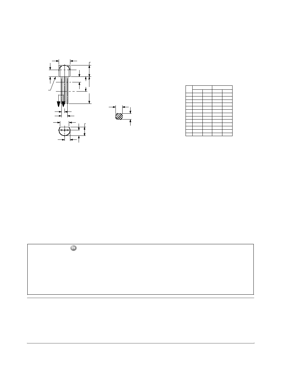
PACKAGE DIMENSIONS
CASE 29≠11
ISSUE AL
TO≠92 (TO≠226)
NOTES:
1. DIMENSIONING AND TOLERANCING PER ANSI
Y14.5M, 1982.
2. CONTROLLING DIMENSION: INCH.
3. CONTOUR OF PACKAGE BEYOND DIMENSION R
IS UNCONTROLLED.
4. LEAD DIMENSION IS UNCONTROLLED IN P AND
BEYOND DIMENSION K MINIMUM.
R
A
P
J
L
B
K
G
H
SECTION X≠X
C
V
D
N
N
X X
SEATING
PLANE
DIM
MIN
MAX
MIN
MAX
MILLIMETERS
INCHES
A
0.175
0.205
4.45
5.20
B
0.170
0.210
4.32
5.33
C
0.125
0.165
3.18
4.19
D
0.016
0.021
0.407
0.533
G
0.045
0.055
1.15
1.39
H
0.095
0.105
2.42
2.66
J
0.015
0.020
0.39
0.50
K
0.500
---
12.70
---
L
0.250
---
6.35
---
N
0.080
0.105
2.04
2.66
P
---
0.100
---
2.54
R
0.115
---
2.93
---
V
0.135
---
3.43
---
1
ON Semiconductor and are trademarks of Semiconductor Components Industries, LLC (SCILLC). SCILLC reserves the right to make changes
without further notice to any products herein. SCILLC makes no warranty, representation or guarantee regarding the suitability of its products for any particular
purpose, nor does SCILLC assume any liability arising out of the application or use of any product or circuit, and specifically disclaims any and all liability,
including without limitation special, consequential or incidental damages. "Typical" parameters which may be provided in SCILLC data sheets and/or
specifications can and do vary in different applications and actual performance may vary over time. All operating parameters, including "Typicals" must be
validated for each customer application by customer's technical experts. SCILLC does not convey any license under its patent rights nor the rights of others.
SCILLC products are not designed, intended, or authorized for use as components in systems intended for surgical implant into the body, or other applications
intended to support or sustain life, or for any other application in which the failure of the SCILLC product could create a situation where personal injury or
death may occur. Should Buyer purchase or use SCILLC products for any such unintended or unauthorized application, Buyer shall indemnify and hold
SCILLC and its officers, employees, subsidiaries, affiliates, and distributors harmless against all claims, costs, damages, and expenses, and reasonable
attorney fees arising out of, directly or indirectly, any claim of personal injury or death associated with such unintended or unauthorized use, even if such claim
alleges that SCILLC was negligent regarding the design or manufacture of the part. SCILLC is an Equal Opportunity/Affirmative Action Employer.
PUBLICATION ORDERING INFORMATION
JAPAN: ON Semiconductor, Japan Customer Focus Center
4≠32≠1 Nishi≠Gotanda, Shinagawa≠ku, Tokyo, Japan 141≠0031
Phone: 81≠3≠5740≠2700
Email: r14525@onsemi.com
ON Semiconductor Website: http://onsemi.com
For additional information, please contact your local
Sales Representative.
J111/D
Thermal Clad is a trademark of the Bergquist Company.
Literature Fulfillment:
Literature Distribution Center for ON Semiconductor
P.O. Box 5163, Denver, Colorado 80217 USA
Phone: 303≠675≠2175 or 800≠344≠3860 Toll Free USA/Canada
Fax: 303≠675≠2176 or 800≠344≠3867 Toll Free USA/Canada
Email: ONlit@hibbertco.com
N. American Technical Support: 800≠282≠9855 Toll Free USA/Canada