 | Электронный компонент: J310ZL1 | Скачать:  PDF PDF  ZIP ZIP |
JFET VHF/UHF Amplifiers
N¡Channel -- Depletion
MAXIMUM RATINGS
Rating
Symbol
Value
Unit
Drain¡Source Voltage
V
DS
25
Vdc
Gate¡Source Voltage
V
GS
25
Vdc
Forward Gate Current
I
GF
10
mAdc
Total Device Dissipation @ T
A
= 25
░
C
Derate above 25
░
C
P
D
350
2.8
mW
mW/
░
C
Junction Temperature Range
T
J
¡65 to +125
░
C
Storage Temperature Range
T
stg
¡65 to +150
░
C
ELECTRICAL CHARACTERISTICS
(T
A
= 25
░
C unless otherwise noted)
Characteristic
Symbol
Min
Typ
Max
Unit
OFF CHARACTERISTICS
Gate¡Source Breakdown Voltage
(I
G
= ¡1.0
╡
Adc, V
DS
= 0)
V
(BR)GSS
¡25
--
--
Vdc
Gate Reverse Current
(V
GS
= ¡15 Vdc, V
DS
= 0, T
A
= 25
░
C)
(V
GS
= ¡15 Vdc, V
DS
= 0, T
A
= +125
░
C)
I
GSS
--
--
--
--
¡1.0
¡1.0
nAdc
╡
Adc
Gate Source Cutoff Voltage
(V
DS
= 10 Vdc, I
D
= 1.0 nAdc)
J308
J309
J310
V
GS(off)
¡1.0
¡1.0
¡2.0
--
--
--
¡6.5
¡4.0
¡6.5
Vdc
ON CHARACTERISTICS
Zero¡Gate¡Voltage Drain Current
(1)
(V
DS
= 10 Vdc, V
GS
= 0)
J308
J309
J310
I
DSS
12
12
24
--
--
--
60
30
60
mAdc
Gate¡Source Forward Voltage
(V
DS
= 0, I
G
= 1.0 mAdc)
V
GS(f)
--
--
1.0
Vdc
ON Semiconductort
⌐
Semiconductor Components Industries, LLC, 2001
March, 2001 ¡ Rev. 1
1
Publication Order Number:
J308/D
J308
J309
J310
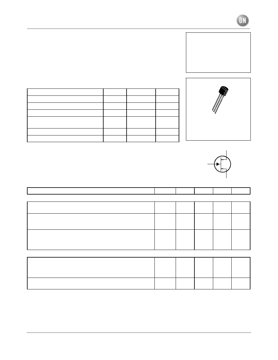
ON Semiconductor Preferred Devices
CASE 29¡11, STYLE 5
TO¡92 (TO¡226AA)
1
2
3
1 DRAIN
2 SOURCE
3
GATE

J308 J309 J310
http://onsemi.com
2
Characteristic
Symbol
Min
Typ
Max
Unit
SMALL¡SIGNAL CHARACTERISTICS
Common¡Source Input Conductance
(V
DS
= 10 Vdc, I
D
= 10 mAdc, f = 100 MHz)
J308
J309
J310
Re(y
is
)
--
--
--
0.7
0.7
0.5
--
--
--
mmhos
Common¡Source Output Conductance
(V
DS
= 10 Vdc, I
D
= 10 mAdc, f = 100 MHz)
Re(y
os
)
--
0.25
--
mmhos
Common¡Gate Power Gain
(V
DS
= 10 Vdc, I
D
= 10 mAdc, f = 100 MHz)
G
pg
--
16
--
dB
1. Pulse Test: Pulse Width
v
300
╡
s, Duty Cycle
v
3.0%.
SMALL¡SIGNAL CHARACTERISTICS (continued)
Common¡Source Forward Transconductance
(V
DS
= 10 Vdc, I
D
= 10 mAdc, f = 100 MHz)
Re(y
fs
)
--
12
--
mmhos
Common¡Gate Input Conductance
(V
DS
= 10 Vdc, I
D
= 10 mAdc, f = 100 MHz)
Re(y
ig
)
--
12
--
mmhos
Common¡Source Forward Transconductance
(V
DS
= 10 Vdc, I
D
= 10 mAdc, f = 1.0 kHz)
J308
J309
J310
g
fs
8000
10000
8000
--
--
--
20000
20000
18000
╡
mhos
Common¡Source Output Conductance
(V
DS
= 10 Vdc, I
D
= 10 mAdc, f = 1.0 kHz)
g
os
--
--
250
╡
mhos
Common¡Gate Forward Transconductance
(V
DS
= 10 Vdc, I
D
= 10 mAdc, f = 1.0 kHz)
J308
J309
J310
g
fg
--
--
--
13000
13000
12000
--
--
--
╡
mhos
Common¡Gate Output Conductance
(V
DS
= 10 Vdc, I
D
= 10 mAdc, f = 1.0 kHz)
J308
J309
J310
g
og
--
--
--
150
100
150
--
--
--
╡
mhos
Gate¡Drain Capacitance
(V
DS
= 0, V
GS
= ¡10 Vdc, f = 1.0 MHz)
C
gd
--
1.8
2.5
pF
Gate¡Source Capacitance
(V
DS
= 0, V
GS
= ¡10 Vdc, f = 1.0 MHz)
C
gs
--
4.3
5.0
pF
FUNCTIONAL CHARACTERISTICS
Noise Figure
(V
DS
= 10 Vdc, I
D
= 10 mAdc, f = 450 MHz)
NF
--
1.5
--
dB
Equivalent Short¡Circuit Input Noise Voltage
(V
DS
= 10 Vdc, I
D
= 10 mAdc, f = 100 Hz)
e
n
--
10
--
nV
Hz
J308 J309 J310
http://onsemi.com
3
C1 = C2 = 0.8 ¡ 10 pF, JFD #MVM010W.
C3 = C4 = 8.35 pF Erie #539¡002D.
C5 = C6 = 5000 pF Erie (2443¡000).
C7 = 1000 pF, Allen Bradley #FA5C.
RFC = 0.33
╡
H Miller #9230¡30.
L1 = One Turn #16 Cu, 1/4
I.D. (Air Core).
L2
P
= One Turn #16 Cu, 1/4
I.D. (Air Core).
L2
S
= One Turn #16 Cu, 1/4
I.D. (Air Core).
50
SOURCE
50
LOAD
U310
C3
C2
C6
C7
C4
1.0 k
RFC
L1
L2
P
L2
S
+V
DD
C1
C5
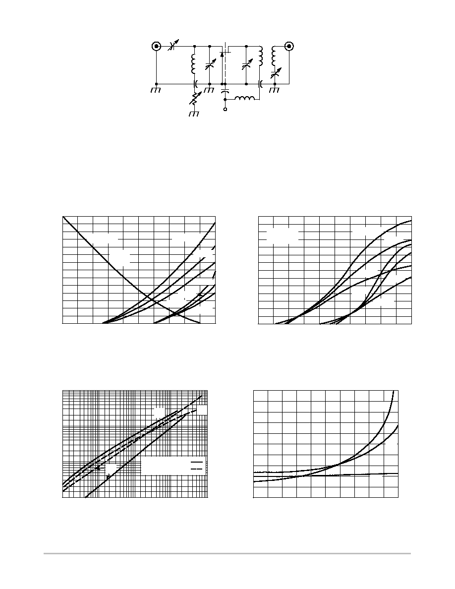
Figure 1. 450 MHz Common¡Gate Amplifier Test Circuit
70
60
50
40
30
20
, SA
TURA
TION DRAIN CURRENT
(mA)
-5.0
-4.0
-3.0
-2.0
-1.0
0
I
D
- V
GS
, GATE-SOURCE VOLTAGE (VOLTS)
I DSS
10
0
70
60
50
40
30
20
10
, DRAIN CURRENT
(mA)
I D
I
DSS
- V
GS
, GATE-SOURCE CUTOFF VOLTAGE (VOLTS)
Figure 2. Drain Current and Transfer
Characteristics versus Gate¡Source Voltage
V
DS
= 10 V
I
DSS
+25
░
C
T
A
= -55
░
C
+25
░
C
+25
░
C
-55
░
C
+150
░
C
+150
░
C
V
GS
, GATE-SOURCE VOLTAGE (VOLTS)
5.0
4.0
3.0
2.0
1.0
0
35
30
25
20
15
10
5.0
0
, FOR
W
ARD
TRANSCONDUCT
ANCE (mmhos)
Y fs
Figure 3. Forward Transconductance
versus Gate¡Source Voltage
V
DS
= 10 V
f = 1.0 MHz
T
A
= -55
░
C
+25
░
C
+150
░
C
+25
░
C
-55
░
C
+150
░
C
I
D
, DRAIN CURRENT (mA)
100 k
10 k
1.0 k
100
1.0 k
100
10
1.0
0.01
0.1 0.2 0.3 0.5 1.0 2.0 3.0 5.0 10 20 30 50 100
, FOR
W
ARD
TRANSCONDUCT
ANCE ( mhos)
Y fs
╡
, OUTPUT
ADMITT
ANCE ( mhos)
Y os
╡
V
GS(off)
= -2.3 V =
V
GS(off)
= -5.7 V =
Figure 4. Common¡Source Output
Admittance and Forward Transconductance
versus Drain Current
Y
fs
Y
fs
Y
os
V
GS
, GATE SOURCE VOLTAGE (VOLTS)
5.0
4.0 3.0
2.0
1.0
0
6.0
7.0
8.0
9.0
10
CAP
ACIT
ANCE (pF)
10
7.0
4.0
1.0
0
120
96
72
48
24
0
, ON RESIST
ANCE (OHMS)
R
DS
R
DS
C
gs
C
gd
Figure 5. On Resistance and Junction
Capacitance versus Gate¡Source Voltage

J308 J309 J310
http://onsemi.com
4
|Y
11
|, |Y
21
|, |Y
22
| (mmhos)
Y 12
(mmhos)
30
24
18
12
6.0
0
1000
100
200
300
500 700
f, FREQUENCY (MHz)
3.0
2.4
1.8
1.2
0.6
|S
21
|, |S
11
|
0.45
0.39
0.33
0.27
0.21
0.15
0.85
0.79
0.73
0.67
0.61
0.55
|S
12
|, |S
22
|
0.060
0.048
0.036
0.024
0.012
1.00
0.98
0.96
0.94
0.92
0.90
1000
100
200
300
500 700
f, FREQUENCY (MHz)
Figure 6. Common¡Gate Y Parameter
Magnitude versus Frequency
Figure 7. Common¡Gate S Parameter
Magnitude versus Frequency
f, FREQUENCY (MHz)
I
D
, DRAIN CURRENT (mA)
NF
, NOISE FIGURE (dB)
NF
, NOISE FIGURE (dB)
G
,
POWER GAIN (dB)
pg
G
,
POWER GAIN (dB)
pg
8.0
7.0
6.0
5.0
4.0
3.0
2.0
1.0
0
4.0 6.0
8.0
10
12
14
16
18
20
22
24
24
21
18
15
12
9.0
6.0
3.0
0
7.0
6.0
5.0
4.0
3.0
2.0
1.0
0
50
100
200 300
500 700 1000
26
22
18
14
10
6.0
2.0
V
DS
= 10 V
I
D
= 10 mA
T
A
= 25
░
C
Y
11
Y
21
Y
22
Y
12
S
22
S
21
S
11
S
12
G
pg
NF
V
DS
= 10 V
I
D
= 10 mA
T
A
= 25
░
C
V
DD
= 20 V
f = 450 MHz
BW
10 MHz
CIRCUIT IN FIGURE 1
V
DS
= 10 V
I
D
= 10 mA
T
A
= 25
░
C
CIRCUIT IN FIGURE 1
G
pg
NF
f, FREQUENCY (MHz)
21
,
11
50
░
40
░
30
░
20
░
10
░
0
░
180
░
170
░
160
░
150
░
140
░
130
░
12
,
22
-2
0
░
-40
░
-80
░
-120
░
-160
░
-200
░
-20
░
-60
░
-100
░
-140
░
-180
░
87
░
86
░
85
░
84
░
83
░
82
░
1000
100
200
300
500
700
Figure 8. Common¡Gate Y Parameter
Phase¡Angle versus Frequency
f, FREQUENCY (MHz)
11
,
12
120
░
100
░
80
░
60
░
40
░
20
░
-20
░
-40
░
-60
░
-80
░
-100
░
-120
░
21
,
22
0
-40
░
-80
░
-20
░
-60
░
-100
░
1000
100
200
300
500
700
Figure 9. S Parameter Phase¡Angle
versus Frequency
22
21
12
11
V
DS
= 10 V
I
D
= 10 mA
T
A
= 25
░
C
11
21
22
21
11
12
V
DS
= 10 V
I
D
= 10 mA
T
A
= 25
░
C
Figure 10. Noise Figure and
Power Gain versus Drain Current
Figure 11. Noise Figure and Power Gain
versus Frequency

J308 J309 J310
http://onsemi.com
5
Figure 12. 450 MHz IMD Evaluation Amplifier
B
W
(3 dB) ¡ 36.5 MHz
I
D
¡ 10 mAdc
V
DS
¡ 20 Vdc
Device case grounded
IM test tones ¡ f1 = 449.5 MHz, f2 = 450.5 MHz
C1 = 1¡10 pF Johanson Air variable trimmer.
C2, C5 = 100 pF feed thru button capacitor.
C3, C4, C6 = 0.5¡6 pF Johanson Air variable trim-
mer.
L1 = 1/8
x 1/32
x 1¡5/8
copper bar.
L2, L4 = Ferroxcube Vk200 choke.
L3 = 1/8
x 1/32
x 1¡7/8
copper bar.
INPUT
R
S
= 50
C1
C2
L1
L2
V
S
S
G
D
SHIELD
C3
U310
C4
V
D
L3
C5
L4
C6
OUTPUT
R
L
= 50
Amplifier power gain and IMD products are a function of the load impedance. For the amplifier design shown above with
C4 and C6 adjusted to reflect a load to the drain resulting in a nominal power gain of 9 dB, the 3rd order intercept point (IP)
value is 29 dBm. Adjusting C4, C6 to provide larger load values will result in higher gain, smaller bandwidth and lower IP
values. For example, a nominal gain of 13 dB can be achieved with an intercept point of 19 dBm.
Example of intercept point plot use:
Assume two in¡band signals of ¡20 dBm at the amplifi-
er input. They will result in a 3rd order IMD signal at
the output of ¡90 dBm. Also, each signal level at the
output will be ¡11 dBm, showing an amplifier gain of
9.0 dB and an intermodulation ratio (IMR) capability
of 79 dB. The gain and IMR values apply only for sig-
nal levels below comparison.
Figure 13. Two Tone 3rd Order Intercept Point
-20
-40
-60
-80
-100
-120
OUTPUT
POWER PER
T
ONE (dBm)
-120
+20
-100
-80
-60
INPUT POWER PER TONE (dBm)
0
+20
+40
-40
-20
0
3RD ORDER INTERCEPT POINT
FUNDAMENTAL OUTPUT
3RD ORDER IMD OUTPUT
U310 JFET
V
DS
= 20 Vdc
I
D
= 10 mAdc
F1 = 449.5 MHz
F2 = 450.5 MHz

J308 J309 J310
http://onsemi.com
6
PACKAGE DIMENSIONS
CASE 29¡11
ISSUE AL
TO¡92 (TO¡226AA)
NOTES:
1. DIMENSIONING AND TOLERANCING PER ANSI
Y14.5M, 1982.
2. CONTROLLING DIMENSION: INCH.
3. CONTOUR OF PACKAGE BEYOND DIMENSION R
IS UNCONTROLLED.
4. LEAD DIMENSION IS UNCONTROLLED IN P AND
BEYOND DIMENSION K MINIMUM.
R
A
P
J
L
B
K
G
H
SECTION X¡X
C
V
D
N
N
X X
SEATING
PLANE
DIM
MIN
MAX
MIN
MAX
MILLIMETERS
INCHES
A
0.175
0.205
4.45
5.20
B
0.170
0.210
4.32
5.33
C
0.125
0.165
3.18
4.19
D
0.016
0.021
0.407
0.533
G
0.045
0.055
1.15
1.39
H
0.095
0.105
2.42
2.66
J
0.015
0.020
0.39
0.50
K
0.500
---
12.70
---
L
0.250
---
6.35
---
N
0.080
0.105
2.04
2.66
P
---
0.100
---
2.54
R
0.115
---
2.93
---
V
0.135
---
3.43
---
1
STYLE 5:
PIN 1. DRAIN
2. SOURCE
3. GATE

J308 J309 J310
http://onsemi.com
7
Notes

J308 J309 J310
http://onsemi.com
8
ON Semiconductor and are trademarks of Semiconductor Components Industries, LLC (SCILLC). SCILLC reserves the right to make changes
without further notice to any products herein. SCILLC makes no warranty, representation or guarantee regarding the suitability of its products for any particular
purpose, nor does SCILLC assume any liability arising out of the application or use of any product or circuit, and specifically disclaims any and all liability,
including without limitation special, consequential or incidental damages. "Typical" parameters which may be provided in SCILLC data sheets and/or
specifications can and do vary in different applications and actual performance may vary over time. All operating parameters, including "Typicals" must be
validated for each customer application by customer's technical experts. SCILLC does not convey any license under its patent rights nor the rights of others.
SCILLC products are not designed, intended, or authorized for use as components in systems intended for surgical implant into the body, or other applications
intended to support or sustain life, or for any other application in which the failure of the SCILLC product could create a situation where personal injury or
death may occur. Should Buyer purchase or use SCILLC products for any such unintended or unauthorized application, Buyer shall indemnify and hold
SCILLC and its officers, employees, subsidiaries, affiliates, and distributors harmless against all claims, costs, damages, and expenses, and reasonable
attorney fees arising out of, directly or indirectly, any claim of personal injury or death associated with such unintended or unauthorized use, even if such claim
alleges that SCILLC was negligent regarding the design or manufacture of the part. SCILLC is an Equal Opportunity/Affirmative Action Employer.
PUBLICATION ORDERING INFORMATION
CENTRAL/SOUTH AMERICA:
Spanish Phone: 303¡308¡7143 (Mon¡Fri 8:00am to 5:00pm MST)
Email: ONlit¡spanish@hibbertco.com
Toll¡Free from Mexico: Dial 01¡800¡288¡2872 for Access ¡
then Dial 866¡297¡9322
ASIA/PACIFIC: LDC for ON Semiconductor ¡ Asia Support
Phone: 1¡303¡675¡2121 (Tue¡Fri 9:00am to 1:00pm, Hong Kong Time)
Toll Free from Hong Kong & Singapore:
001¡800¡4422¡3781
Email: ONlit¡asia@hibbertco.com
JAPAN: ON Semiconductor, Japan Customer Focus Center
4¡32¡1 Nishi¡Gotanda, Shinagawa¡ku, Tokyo, Japan 141¡0031
Phone: 81¡3¡5740¡2700
Email: r14525@onsemi.com
ON Semiconductor Website: http://onsemi.com
For additional information, please contact your local
Sales Representative.
J308/D
NORTH AMERICA Literature Fulfillment:
Literature Distribution Center for ON Semiconductor
P.O. Box 5163, Denver, Colorado 80217 USA
Phone: 303¡675¡2175 or 800¡344¡3860 Toll Free USA/Canada
Fax: 303¡675¡2176 or 800¡344¡3867 Toll Free USA/Canada
Email: ONlit@hibbertco.com
Fax Response Line: 303¡675¡2167 or 800¡344¡3810 Toll Free USA/Canada
N. American Technical Support: 800¡282¡9855 Toll Free USA/Canada
EUROPE: LDC for ON Semiconductor ¡ European Support
German Phone: (+1) 303¡308¡7140 (Mon¡Fri 2:30pm to 7:00pm CET)
Email: ONlit¡german@hibbertco.com
French Phone: (+1) 303¡308¡7141 (Mon¡Fri 2:00pm to 7:00pm CET)
Email: ONlit¡french@hibbertco.com
English Phone: (+1) 303¡308¡7142 (Mon¡Fri 12:00pm to 5:00pm GMT)
Email: ONlit@hibbertco.com
EUROPEAN TOLL¡FREE ACCESS*: 00¡800¡4422¡3781
*Available from Germany, France, Italy, UK, Ireland