 | ÐлекÑÑоннÑй компоненÑ: LM211DR2 | СкаÑаÑÑ:  PDF PDF  ZIP ZIP |
LM211
©
Semiconductor Components Industries, LLC, 2002
May, 2002 Rev. 2
1
Publication Order Number:
LM211/D
LM211, LM311
Single Comparators
The ability to operate from a single power supply of 5.0 V to 30 V or
$15 V split supplies, as commonly used with operational amplifiers,
makes the LM211/LM311 a truly versatile comparator. Moreover, the
inputs of the device can be isolated from system ground while the
output can drive loads referenced either to ground, the V
CC
or the V
EE
supply. This flexibility makes it possible to drive DTL, RTL, TTL, or
MOS logic. The output can also switch voltages to 50 V at currents to
50 mA, therefore, the LM211/LM311 can be used to drive relays,
lamps or solenoids.
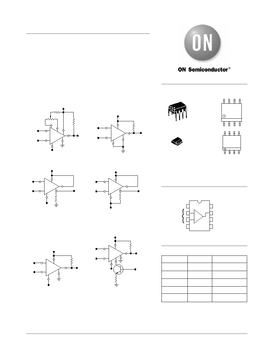
Figure 1. Typical Comparator Design Configurations
Split Power Supply with Offset Balance
Single Supply
GroundReferred Load
Load Referred to Positive Supply
Strobe Capability
Output
V
EE
Inputs
V
CC
R
L
1
2
3
4
5
6
7
8
5.0 k
3.0 k
V
CC
V
CC
V
CC
V
CC
V
CC
Output
Output
Output
Output
Output
R
L
R
L
R
L
R
L
R
L
Inputs
Inputs
Inputs
Inputs
Inputs
V
EE
V
EE
V
EE
V
EE
V
EE
2
3
2
3
2
3
2
3
2
3
4
4
4
4
4
7
8
1
Input polarity is reversed when
Gnd pin is used as an output.
7
1
8
8
7
6
1
1.0 k
TTL Strobe
1
7
8
Load Referred to Negative Supply
1
7
8
Input polarity is reversed when
Gnd pin is used as an output.
+
+
+
+
+
+
-
Device
Package
Shipping
ORDERING INFORMATION
LM211D
SO8
98 Units/Rail
LM311D
SO8
PDIP8
N SUFFIX
CASE 626
1
8
98 Units/Rail
SO8
D SUFFIX
CASE 751
1
8
LM211DR2
SO8
2500 Tape & Reel
MARKING
DIAGRAMS
ALYW
LMx11
1
8
x
= 2 or 3
A
= Assembly Location
WL, L
= Wafer Lot
YY, Y
= Year
WW, W = Work Week
AWL
LM311N
1
8
YYWW
Gnd
Inputs
V
EE
V
CC
Output
Balance/Strobe
Balance
(Top View)
1
2
3
4
8
7
6
5
PIN CONNECTIONS
+
LM311DR2
SO8
2500 Tape & Reel
LM311N
PDIP8
50 Units/Rail
http://onsemi.com
LM211, LM311
http://onsemi.com
2
MAXIMUM RATINGS
(T
A
= +25
°
C, unless otherwise noted.)
Rating
Symbol
LM211
LM311
Unit
Total Supply Voltage
V
CC
+
V
EE
36
36
Vdc
Output to Negative Supply Voltage
V
O
V
EE
50
40
Vdc
Ground to Negative Supply Voltage
V
EE
30
30
Vdc
Input Differential Voltage
V
ID
±
30
±
30
Vdc
Input Voltage (Note 2)
V
in
±
15
±
15
Vdc
Voltage at Strobe Pin
V
CC
to V
CC
5
V
CC
to V
CC
5
Vdc
Power Dissipation and Thermal Characteristics
Plastic DIP
P
D
625
mW
Derate Above T
A
= +25
°
C
R
q
JA
5.0
mW/
°
C
Operating Ambient Temperature Range
T
A
25 to +85
0 to +70
°
C
Operating Junction Temperature
T
J(max)
+150
+150
°
C
Storage Temperature Range
T
stg
65 to +150
65 to +150
°
C
ELECTRICAL CHARACTERISTICS
(V
CC
= +15 V, V
EE
= 15 V, T
A
= 25
°
C, unless otherwise noted [Note 1])
LM211
LM311
Characteristic
Symbol
Min
Typ
Max
Min
Typ
Max
Unit
Input Offset Voltage (Note 3)
V
IO
mV
R
S
50 k
W
, T
A
= +25
°
C
0.7
3.0
2.0
7.5
R
S
50 k
W
, T
low
T
A
T
high
*
4.0
10
Input Offset Current (Note 3) T
A
= +25
°
C
I
IO
1.7
10
1.7
50
nA
T
low
T
A
T
high
*
20
70
Input Bias Current T
A
= +25
°
C
I
IB
45
100
45
250
nA
T
low
T
A
T
high
*
150
300
Voltage Gain
A
V
40
200
40
200
V/mV
Response Time (Note 4)
200
200
ns
Saturation Voltage
V
OL
V
V
ID
5.0 mV, I
O
= 50 mA, T
A
= 25
°
C
0.75
1.5
V
ID
10 mV, I
O
= 50 mA, T
A
= 25
°
C
0.75
1.5
V
CC
4.5 V, V
EE
= 0, T
low
T
A
T
high
*
V
ID
6
6.0 mV, I
sink
8.0 mA
0.23
0.4
V
ID
6
10 mV, I
sink
8.0 mA
0.23
0.4
Strobe "On" Current (Note 5)
I
S
3.0
3.0
mA
Output Leakage Current
V
ID
5.0 mV,
V
O
= 35 V, T
A
= 25
°
C, I
strobe
= 3.0 mA
0.2
10
nA
V
ID
10 mV,
V
O
= 35 V, T
A
= 25
°
C, I
strobe
= 3.0 mA
0.2
50
nA
V
ID
5.0 mV,
V
O
= 35 V, T
low
T
A
T
high
*
0.1
0.5
m
A
Input Voltage Range (T
low
T
A
T
high
*)
V
ICR
14.5
14.7 to
13.8
+13.0
14.5
14.7 to
13.8
+13.0
V
Positive Supply Current
I
CC
+2.4
+6.0
+2.4
+7.5
mA
Negative Supply Current
I
EE
1.3
5.0
1.3
5.0
mA
* LM211: T
low
= 25
°
C, T
high
= +85
°
C
LM311: T
low
= 0
°
C, T
high
= +70
°
C
1. Offset voltage, offset current and bias current specifications apply for a supply voltage range from a single 5.0 V supply up to
±
15 V supplies.
2. This rating applies for
±
15 V supplies. The positive input voltage limit is 30 V above the negative supply. The negative input voltage limit is
equal to the negative supply voltage or 30 V below the positive supply, whichever is less.
3. The offset voltages and offset currents given are the maximum values required to drive the output within a volt of either supply with a 1.0 mA
load. Thus, these parameters define an error band and take into account the "worst case" effects of voltage gain and input impedance.
4. The response time specified is for a 100 mV input step with 5.0 mV overdrive.
5. Do not short the strobe pin to ground; it should be current driven at 3.0 mA to 5.0 mA.
LM211, LM311
http://onsemi.com
3
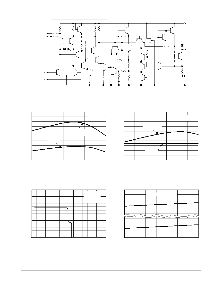
Figure 2. Circuit Schematic
Figure 3. Input Bias Current
versus Temperature
Figure 4. Input Offset Current
versus Temperature
Figure 5. Input Bias Current versus
Differential Input Voltage
Figure 6. Common Mode Limits
versus Temperature
T
A
, TEMPERATURE (
°
C)
T
A
, TEMPERATURE (
°
C)
DIFFERENTIAL INPUT VOLTAGE (V)
I IB
, INPUT
BIAS CURRENT
(nA)
I IO
, INPUT
OFFSET
CURRENT
(nA)
COMMON MODE LIMITS (V)
140
120
100
80
40
0
140
120
100
80
40
0
60
20
-55
-25
0
25
50
75
100
125
-16
-12
-8.0
-4.0
0
4.0
8.0
12
16
5.0
4.0
3.0
2.0
1.0
0
-55
-25
0
25
50
75
100
125
-55
-25
0
25
50
75
100
125
V
CC
-0.5
-1.0
-1.5
0.4
0.2
V
EE
8
7
1
4
V
EE
Gnd
Output
V
CC
5.0 k
200
600
3.0 k
300
900
800
5.4 k
1.3 k
250
800
800
100
3.7 k
730 340
3.7 k
300
5
6
300
2
3
Inputs
1.3 k
1.3 k
1.3 k
Balance
Balance/Strobe
T
A
, TEMPERATURE (
°
C)
Normal
V
CC
= +15 V
V
EE
= -15 V
I IB
, INPUT
BIAS CURRENT
(nA)
Referred to Supply Voltages
V
CC
= +15 V
V
EE
= -15 V
T
A
= +25
°
C
Normal
Pins 5 & 6 Tied
to V
CC
V
CC
= +15 V
V
EE
= -15 V
Pins 5 & 6 Tied
to V
CC
LM211, LM311
http://onsemi.com
4
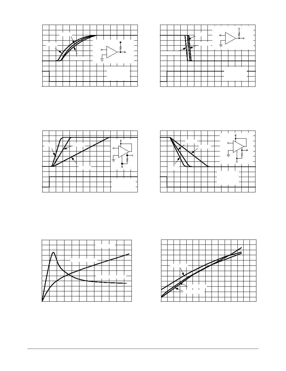
Figure 7. Response Time for
Various Input Overdrives
Figure 8. Response Time for
Various Input Overdrives
Figure 9. Response Time for
Various Input Overdrives
Figure 10. Response Time for
Various Input Overdrives
Figure 11. Output Short Circuit Current
Characteristics and Power Dissipation
Figure 12. Output Saturation Voltage
versus Output Current
t
TLH
, RESPONSE TIME (ms)
t
THL
, RESPONSE TIME (ms)
t
TLH
, RESPONSE TIME (ms)
t
THL
, RESPONSE TIME (ms)
V
O
, OUTPUT VOLTAGE (V)
I
O
, OUTPUT CURRENT (mA)
V in
INPUT
VOL
T
AGE (mV)
,
V O
, OUTPUT
VOL
T
AGE (V)
V in
INPUT
VOL
T
AGE (mV)
,
V O
, OUTPUT
VOL
T
AGE (V)
V in
INPUT
VOL
T
AGE (mV)
,
V O
, OUTPUT
VOL
T
AGE (V)
V in
INPUT
VOL
T
AGE (mV)
,
V O
, OUTPUT
VOL
T
AGE (V)
OUTPUT
SHOR
T
CIRCUIT
CURRENT
(mA)
V OL
, SA
TURA
TION VOL
T
AGE (V)
P D
, POWER DISSIP
A
TION (W)
5.0
4.0
3.0
2.0
1.0
0
0
50
100
0
0.1
0.2
0.3
0.4
0.5
0.6
5.0
4.0
3.0
2.0
1.0
0
-100
-50
0
0
0.1
0.2
0.3
0.4
0.5
0.6
15
10
5.0
0
-5.0
-10
-15
0
-50
-100
0
1.0
2.0
0
1.0
2.0
15
10
5.0
0
-5.0
-10
-15
0
50
100
150
125
100
75
50
25
0
0
5.0
10
15
0.90
0.75
0.60
0.45
0.30
0.15
0
0.90
0.75
0.60
0.45
0.30
0.15
0
0
8.0
16
24
32
40
48
56
T
A
= +25
°
C
T
A
= -55
°
C
T
A
= +25
°
C
T
A
= +125
°
C
5.0 mV
20 mV
2.0 mV
V
in
+5.0 V
500 W
V
O
*
)
+5.0 V
500 W
V
O
V
in
20 mV
5.0 mV
20 mV
5.0 mV
2.0 mV
V
in
V
CC
V
O
2.0 k
V
EE
*
)
20 mV
5.0 mV
2.0 mV
V
in
V
CC
V
O
2.0 k
V
EE
*
)
*
)
Power Dissipation
Short Circuit Current
2.0 mV
V
CC
= +15 V
V
EE
= -15 V
T
A
= +25
°
C
V
CC
= +15 V
V
EE
= -15 V
T
A
= +25
°
C
V
CC
= +15 V
V
EE
= -15 V
T
A
= +25
°
C
V
CC
= +15 V
V
EE
= -15 V
T
A
= +25
°
C
LM211, LM311
http://onsemi.com
5
8
8
Figure 13. Output Leakage Current
versus Temperature
Figure 14. Power Supply Current
versus Supply Voltage
Figure 15. Power Supply Current
versus Temperature
APPLICATIONS INFORMATION
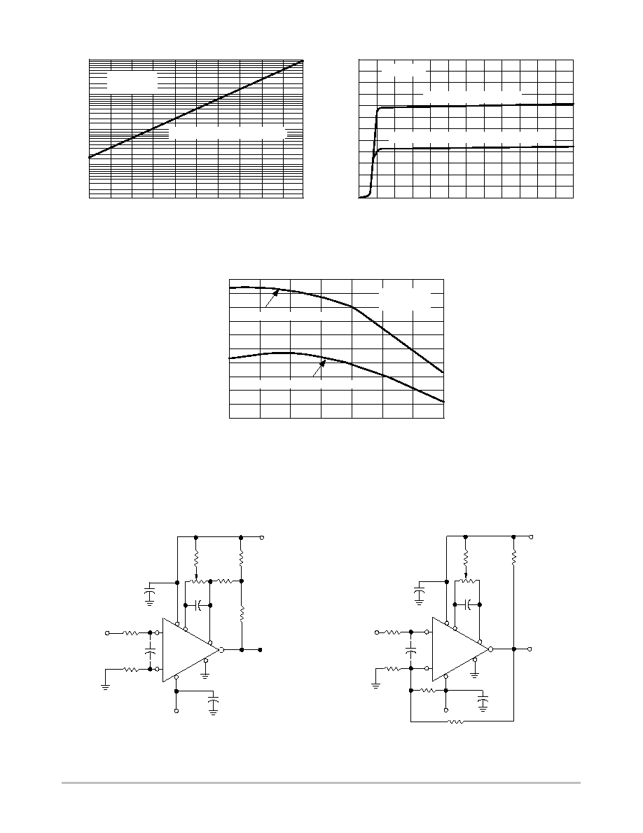
Figure 16. Improved Method of Adding
Hysteresis Without Applying Positive
Feedback to the Inputs
Figure 17. Conventional Technique
for Adding Hysteresis
OUTPUT
LEAKAGE CURRENT
(mA)
POWER SUPPL
Y
CURRENT
(mA)
SUPPL
Y
CURRENT
(mA)
T
A
, TEMPERATURE (
°
C)
T
A
, TEMPERATURE (
°
C)
V
CC
-V
EE
, POWER SUPPLY VOLTAGE (V)
100
10
1.0
0.1
0.01
25
45
65
85
105
125
3.6
3.0
2.4
1.8
1.2
0.6
0
0
5.0
10
15
20
25
30
2.2
1.8
1.4
1.0
-55
-25
0
25
50
75
100
125
Positive and Negative Supply - Output High
Postive Supply - Output Low
+15 V
82
3.0 k
33 k
5.0 k
C1
0.002
mF
6
2
R1
R2
C2
Input
3
4
1 7
-15 V
5
4.7 k
LM311
0.1 mF
Output
+
-
0.1 mF
+15 V
3.0 k
5.0 k
C1
6
3
R1
R2
C2
Input
2
4
1 7
-15 V
5
4.7 k
LM311
0.1 mF
Output
+
-
0.1 mF
510 k
1.0 M
100
100
3.0
2.6
V
CC
= +15 V
V
EE
= -15 V
T
A
= +25
°
C
Output V
O
= +50 V (LM211 only)
Positive Supply - Output Low
Positive and Negative Power Supply - Output H igh
V
CC
= +15 V
V
EE
= -15 V