©
Semiconductor Components Industries, LLC, 2001
November, 2001 ≠ Rev. 1
1
Publication Order Number:
M1MA174T1/D
M1MA174T1
Preferred Device
Silicon Switching Diode
MAXIMUM RATINGS
Rating
Symbol
Value
Unit
Continuous Reverse Voltage
VR
100
V
Recurrent Peak Forward Current
IF
200
mA
Peak Forward Surge Current
Pulse Width = 10
µ
s
IFM(surge)
500
mA
Total Power Dissipation,
One Diode Loaded
TA = 25
∞
C
Derate above 25
∞
C
Mounted on a Ceramic Substrate
(10 x 8 x 0.6 mm)
PD
200
1.6
mW
mW/
∞
C
Operating and Storage Junction
Temperature Range
TJ, Tstg
≠55 to
+150
∞
C
THERMAL CHARACTERISTICS
Characteristic
Symbol
Max
Unit
Thermal Resistance,
Junction to Ambient
One Diode Loaded
Mounted on a Ceramic Substrate
(10 x 8 x 0.6 mm)
R
JA
0.625
∞
C/mW
ELECTRICAL CHARACTERISTICS
(TA = 25
∞
C unless otherwise noted)
Characteristic
Symbol
Min
Max
Unit
Reverse Breakdown Voltage
(IR = 100
µ
Adc)
V(BR)
100
≠
Vdc
Reverse Voltage Leakage Current
(VR = 20 Vdc)
(VR = 75 Vdc)
IR
≠
≠
25
5.0
nAdc
µ
Adc
Diode Capacitance
(VR = 0, f = 1.0 MHz)
CT
≠
4.0
pF
Forward Voltage
(IF = 10 mAdc)
VF
≠
1.0
Vdc
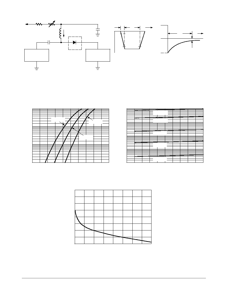
Reverse Recovery Time
(IF = IR = 10 mAdc) (Figure 1)
trr
≠
4.0
ns
Device
Package
Shipping
ORDERING INFORMATION
SC≠70/SOT≠323
CASE 419
STYLE 2
http://onsemi.com
M1MA174T1
SC≠70
3000/Tape & Reel
MARKING DIAGRAM
J6 M
J6
= Device Code
M
= Date Code
Preferred devices are recommended choices for future use
and best overall value.
3
CATHODE
1
ANODE
2
1
3
M1MA174T1
http://onsemi.com
2
Notes: 1. A 2.0 k
variable resistor adjusted for a Forward Current (IF) of 10 mA.
Notes:
2. Input pulse is adjusted so IR(peak) is equal to 10 mA.
Notes:
3. tp ª trr
+10 V
2.0 k
820
0.1
µ
F
DUT
VR
100
µ
H
0.1
µ
F
50
OUTPUT
PULSE
GENERATOR
50
INPUT
SAMPLING
OSCILLOSCOPE
tr
tp
t
10%
90%
IF
IR
trr
t
iR(REC) = 1.0 mA
OUTPUT PULSE
(IF = IR = 10 mA; MEASURED
at iR(REC) = 1.0 mA)
IF
INPUT SIGNAL
Figure 1. Recovery Time Equivalent Test Circuit
Figure 2. Forward Voltage
VF, FORWARD VOLTAGE (VOLTS)
1.0
10
100
0.1
Figure 3. Leakage Current
VR, REVERSE VOLTAGE (VOLTS)
10
0
I
1.0
0.1
0.001
0.01
10
20
30
40
50
I
1.0
1.2
0.2
0.4
0.6
0.8
Figure 4. Capacitance
VR, REVERSE VOLTAGE (VOLTS)
0
C
0.68
0.64
0.60
0.52
0.56
2.0
4.0
6.0
8.0
, FOR
W
ARD CURRENT
(mA)
F
TA = 85
∞
C
TA = -40
∞
C
TA = 25
∞
C
, REVERSE CURRENT
(
A)
R
m
, DIODE CAP
ACIT
ANCE (pF)
D
TA = 25
∞
C
TA = 55
∞
C
TA = 85
∞
C
TA = 150
∞
C
TA = 125
∞
C

M1MA174T1
http://onsemi.com
3
PD =
TJ(max) ≠ TA
R
JA
PD =
150
∞
C ≠ 25
∞
C
0.625
∞
C/W
= 200 milliwatts
∑
The soldering temperature and time should not exceed
260
∞
C for more than 10 seconds.
∑
When shifting from preheating to soldering, the
maximum temperature gradient should be 5
∞
C or less.
∑
After soldering has been completed, the device should
be allowed to cool naturally for at least three minutes.
Gradual cooling should be used as the use of forced
cooling will increase the temperature gradient and
result in latent failure due to mechanical stress.
∑
Mechanical stress or shock should not be applied dur-
ing cooling
* Soldering a device without preheating can cause exces-
sive thermal shock and stress which can result in damage
to the device.
INFORMATION FOR USING THE SC≠70/SOT≠323 SURFACE MOUNT PACKAGE
MINIMUM RECOMMENDED FOOTPRINT FOR SURFACE MOUNTED APPLICATIONS
Surface mount board layout is a critical portion of the total
design. The footprint for the semiconductor packages must
be the correct size to insure proper solder connection
SC≠70/SOT≠323 POWER DISSIPATION
The power dissipation of the SC≠70/SOT≠323 is a func-
tion of the pad size. This can vary from the minimum pad
size for soldering to the pad size given for maximum power
dissipation. Power dissipation for a surface mount device
is determined by TJ(max), the maximum rated junction tem-
perature of the die, R
JA, the thermal resistance from the
device junction to ambient; and the operating temperature,
TA. Using the values provided on the data sheet, PD can be
calculated as follows.
The values for the equation are found in the maximum
ratings table on the data sheet. Substituting these values into
the equation for an ambient temperature TA of 25
∞
C, one
can calculate the power dissipation of the device which in
this case is 200 milliwatts.
The 0.625
∞
C/W assumes the use of the recommended
footprint on a glass epoxy printed circuit board to achieve
a power dissipation of 200 milliwatts. Another alternative
would be to use a ceramic substrate or an aluminum core
board such as Thermal Clad
TM
. Using a board material such
as Thermal Clad, a higher power dissipation of 300 milli-
watts can be achieved using the same footprint.
interface between the board and the package. With the
correct pad geometry, the packages will self align when
subjected to a solder reflow process.
SOLDERING PRECAUTIONS
The melting temperature of solder is higher than the rated
temperature of the device. When the entire device is heated
to a high temperature, failure to complete soldering within
a short time could result in device failure. Therefore, the
following items should always be observed in order to
minimize the thermal stress to which the devices are
subjected.
∑
Always preheat the device.
∑
The delta temperature between the preheat and
soldering should be 100
∞
C or less.*
∑
When preheating and soldering, the temperature of the
leads and the case must not exceed the maximum
temperature ratings as shown on the data sheet. When
using infrared heating with the reflow soldering
method, the difference should be a maximum of 10
∞
C.
mm
inches
0.035
0.9
0.075
0.7
1.9
0.028
0.65
0.025
0.65
0.025

M1MA174T1
http://onsemi.com
4
STEP 1
PREHEAT
ZONE 1
RAMP"
STEP 2
VENT
SOAK"
STEP 3
HEATING
ZONES 2 & 5
RAMP"
STEP 4
HEATING
ZONES 3 & 6
SOAK"
STEP 5
HEATING
ZONES 4 & 7
SPIKE"
STEP 6
VENT
STEP 7
COOLING
200
∞
C
150
∞
C
100
∞
C
50
∞
C
TIME (3 TO 7 MINUTES TOTAL)
TMAX
SOLDER IS LIQUID FOR
40 TO 80 SECONDS
(DEPENDING ON
MASS OF ASSEMBLY)
205
∞
TO 219
∞
C
PEAK AT
SOLDER JOINT
DESIRED CURVE FOR LOW
MASS ASSEMBLIES
100
∞
C
150
∞
C
160
∞
C
140
∞
C
Figure 5. Typical Solder Heating Profile
DESIRED CURVE FOR HIGH
MASS ASSEMBLIES
170
∞
C
For any given circuit board, there will be a group of
control settings that will give the desired heat pattern. The
operator must set temperatures for several heating zones,
and a figure for belt speed. Taken together, these control
settings make up a heating "profile" for that particular
circuit board. On machines controlled by a computer, the
computer remembers these profiles from one operating
session to the next. Figure 7 shows a typical heating profile
for use when soldering a surface mount device to a printed
circuit board. This profile will vary among soldering
systems but it is a good starting point. Factors that can
affect the profile include the type of soldering system in
use, density and types of components on the board, type of
solder used, and the type of board or substrate material
being used. This profile shows temperature versus time.
SOLDER STENCIL GUIDELINES
Prior to placing surface mount components onto a printed
circuit board, solder paste must be applied to the pads. A
solder stencil is required to screen the optimum amount of
solder paste onto the footprint. The stencil is made of brass
or stainless steel with a typical thickness of 0.008 inches.
The stencil opening size for the surface mounted package
should be the same as the pad size on the printed circuit
board, i.e., a 1:1 registration.
TYPICAL SOLDER HEATING PROFILE
The line on the graph shows the actual temperature that
might be experienced on the surface of a test board at or
near a central solder joint. The two profiles are based on a
high density and a low density board. The Vitronics
SMD310 convection/infrared reflow soldering system was
used to generate this profile. The type of solder used was
62/36/2 Tin Lead Silver with a melting point between
177≠189
∞
C. When this type of furnace is used for solder
reflow work, the circuit boards and solder joints tend to
heat first. The components on the board are then heated by
conduction. The circuit board, because it has a large surface
area, absorbs the thermal energy more efficiently, then
distributes this energy to the components. Because of this
effect, the main body of a component may be up to 30
degrees cooler than the adjacent solder joints.

M1MA174T1
http://onsemi.com
5
PACKAGE DIMENSIONS
SC≠70 (SOT≠323)
CASE 419≠04
ISSUE L
C
N
A
L
D
G
S
B
H
J
K
3
1
2
NOTES:
1. DIMENSIONING AND TOLERANCING PER ANSI
Y14.5M, 1982.
2. CONTROLLING DIMENSION: INCH.
DIM
MIN
MAX
MIN
MAX
MILLIMETERS
INCHES
A
0.071
0.087
1.80
2.20
B
0.045
0.053
1.15
1.35
C
0.032
0.040
0.80
1.00
D
0.012
0.016
0.30
0.40
G
0.047
0.055
1.20
1.40
H
0.000
0.004
0.00
0.10
J
0.004
0.010
0.10
0.25
K
0.017 REF
0.425 REF
L
0.026 BSC
0.650 BSC
N
0.028 REF
0.700 REF
S
0.079
0.095
2.00
2.40
0.05 (0.002)
STYLE 2:
PIN 1. ANODE
2. N.C.
3. CATHODE

M1MA174T1
http://onsemi.com
6
Notes

M1MA174T1
http://onsemi.com
7
Notes
M1MA174T1
http://onsemi.com
8
ON Semiconductor and are trademarks of Semiconductor Components Industries, LLC (SCILLC). SCILLC reserves the right to make changes
without further notice to any products herein. SCILLC makes no warranty, representation or guarantee regarding the suitability of its products for any particular
purpose, nor does SCILLC assume any liability arising out of the application or use of any product or circuit, and specifically disclaims any and all liability,
including without limitation special, consequential or incidental damages. "Typical" parameters which may be provided in SCILLC data sheets and/or
specifications can and do vary in different applications and actual performance may vary over time. All operating parameters, including "Typicals" must be
validated for each customer application by customer's technical experts. SCILLC does not convey any license under its patent rights nor the rights of others.
SCILLC products are not designed, intended, or authorized for use as components in systems intended for surgical implant into the body, or other applications
intended to support or sustain life, or for any other application in which the failure of the SCILLC product could create a situation where personal injury or
death may occur. Should Buyer purchase or use SCILLC products for any such unintended or unauthorized application, Buyer shall indemnify and hold
SCILLC and its officers, employees, subsidiaries, affiliates, and distributors harmless against all claims, costs, damages, and expenses, and reasonable
attorney fees arising out of, directly or indirectly, any claim of personal injury or death associated with such unintended or unauthorized use, even if such claim
alleges that SCILLC was negligent regarding the design or manufacture of the part. SCILLC is an Equal Opportunity/Affirmative Action Employer.
PUBLICATION ORDERING INFORMATION
JAPAN: ON Semiconductor, Japan Customer Focus Center
4≠32≠1 Nishi≠Gotanda, Shinagawa≠ku, Tokyo, Japan 141≠0031
Phone: 81≠3≠5740≠2700
Email: r14525@onsemi.com
ON Semiconductor Website: http://onsemi.com
For additional information, please contact your local
Sales Representative.
M1MA174T1/D
Thermal Clad is a trademark of the Bergquist Company.
Literature Fulfillment:
Literature Distribution Center for ON Semiconductor
P.O. Box 5163, Denver, Colorado 80217 USA
Phone: 303≠675≠2175 or 800≠344≠3860 Toll Free USA/Canada
Fax: 303≠675≠2176 or 800≠344≠3867 Toll Free USA/Canada
Email: ONlit@hibbertco.com
N. American Technical Support: 800≠282≠9855 Toll Free USA/Canada