©
Semiconductor Components Industries, LLC, 2002
October, 2002 ≠ Rev. 1
1
Publication Order Number:
MBR120ESFT1/D
MBR120ESFT1
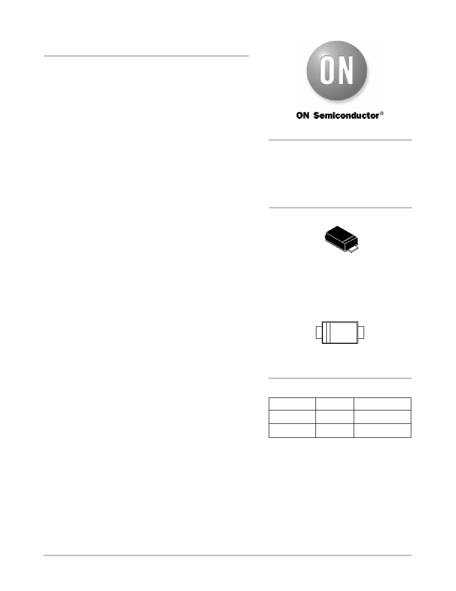
Surface Mount
Schottky Power Rectifier
Plastic SOD≠123 Package
. . . using the Schottky Barrier principle with a large area
metal≠to≠silicon power diode. Ideally suited for low voltage, high
frequency rectification or as free wheeling and polarity protection
diodes in surface mount applications where compact size and weight
are critical to the system. This package also provides an easy to work
with alternative to leadless 34 package style. Because of its small size,
it is ideal for use in portable and battery powered products such as
cellular and cordless phones, chargers, notebook computers, printers,
PDAs and PCMCIA cards. Typical applications are ac/dc and dc≠dc
converters, reverse battery protection, and "Oring" of multiple supply
voltages and any other application where performance and size are
critical. These state≠of≠the≠art devices have the following features:
∑
Guardring for Stress Protection
∑
Low Leakage
∑
150
∞
C Operating Junction Temperature
∑
Epoxy Meets UL94, V0 at 1/8
∑
Package Designed for Optimal Automated Board Assembly
∑
ESD Ratings: Machine Model, C
ESD Ratings:
Human Body Model, 3B
Mechanical Characteristics
∑
Reel Options: MBR120ESFT1 = 3,000 per 7
reel/8 mm tape
Reel Options:
MBR120ESFT3 = 10,000 per 13
reel/8 mm tape
∑
Device Marking: L2E
∑
Polarity Designator: Cathode Band
∑
Weight: 11.7 mg (approximately)
∑
Case: Epoxy, Molded
∑
Finish: All External Surfaces Corrosion Resistant and Terminal
Leads are Readily Solderable
∑
Lead and Mounting Surface Temperature for Soldering Purposes:
260
∞
C Max. for 10 Seconds
Device
Package
Shipping
ORDERING INFORMATION
MBR120ESFT1 SOD≠123FL
SOD≠123FL
CASE 498
PLASTIC
3000/Tape & Reel
SCHOTTKY BARRIER
RECTIFIER
1.0 AMPERES
20 VOLTS
MBR120ESFT3 SOD≠123FL 10,000/Tape & Reel
DEVICE MARKING
L2E
D
L2E
= Specific Device Code
D
= Date Code
http://onsemi.com

MBR120ESFT1
http://onsemi.com
2
MAXIMUM RATINGS
Rating
Symbol
Value
Unit
Peak Repetitive Reverse Voltage
Working Peak Reverse Voltage
DC Blocking Voltage
V
RRM
V
RWM
V
R
20
V
Average Rectified Forward Current (At Rated V
R
, T
L
= 140
∞
C)
I
O
1.0
A
Peak Repetitive Forward Current
(At Rated V
R
, Square Wave, 20 kHz, T
L
= 125
∞
C)
I
FRM
2.0
A
Non≠Repetitive Peak Surge Current
(Non≠Repetitive peak surge current, halfwave, single phase, 60 Hz)
I
FSM
40
A
Storage Temperature
T
stg
≠65 to 150
∞
C
Operating Junction Temperature
T
J
≠65 to 150
∞
C
Voltage Rate of Change (Rated V
R
, T
J
= 25
∞
C)
dv/dt
10,000
V/
m
s
THERMAL CHARACTERISTICS
Thermal Resistance ≠ Junction≠to≠Lead (Note 1)
Thermal Resistance ≠ Junction≠to≠Lead (Note 2)
Thermal Resistance ≠ Junction≠to≠Ambient (Note 1)
Thermal Resistance ≠ Junction≠to≠Ambient (Note 2)
R
tjl
R
tjl
R
tja
R
tja
26
21
325
82
∞
C/W
1. Mounted with minimum recommended pad size, PC Board FR4.
2. Mounted with 1 in. copper pad (Cu area 700 mm
2
).
ELECTRICAL CHARACTERISTICS
Maximum Instantaneous Forward Voltage (Note 3), See Figure 2
V
F
T
J
= 25
∞
C
T
J
= 100
∞
C
V
(I
F
= 0.1 A)
(I
F
= 1.0 A)
(I
F
= 2.0 A)
0.455
0.530
0.595
0.360
0.455
0.540
Maximum Instantaneous Reverse Current (Note 3), See Figure 4
I
R
T
J
= 25
∞
C
T
J
= 100
∞
C
m
A
(V
R
= 20 V)
(V
R
= 10 V)
(V
R
= 5.0 V)
10
1.0
0.5
1600
500
300
3. Pulse Test: Pulse Width
250
µ
s, Duty Cycle
2%.
i
F
, INST
ANT
ANEOUS FOR
W
ARD CURRENT (AMPS)
i
F
, INST
ANT
ANEOUS FOR
W
ARD CURRENT (AMPS)
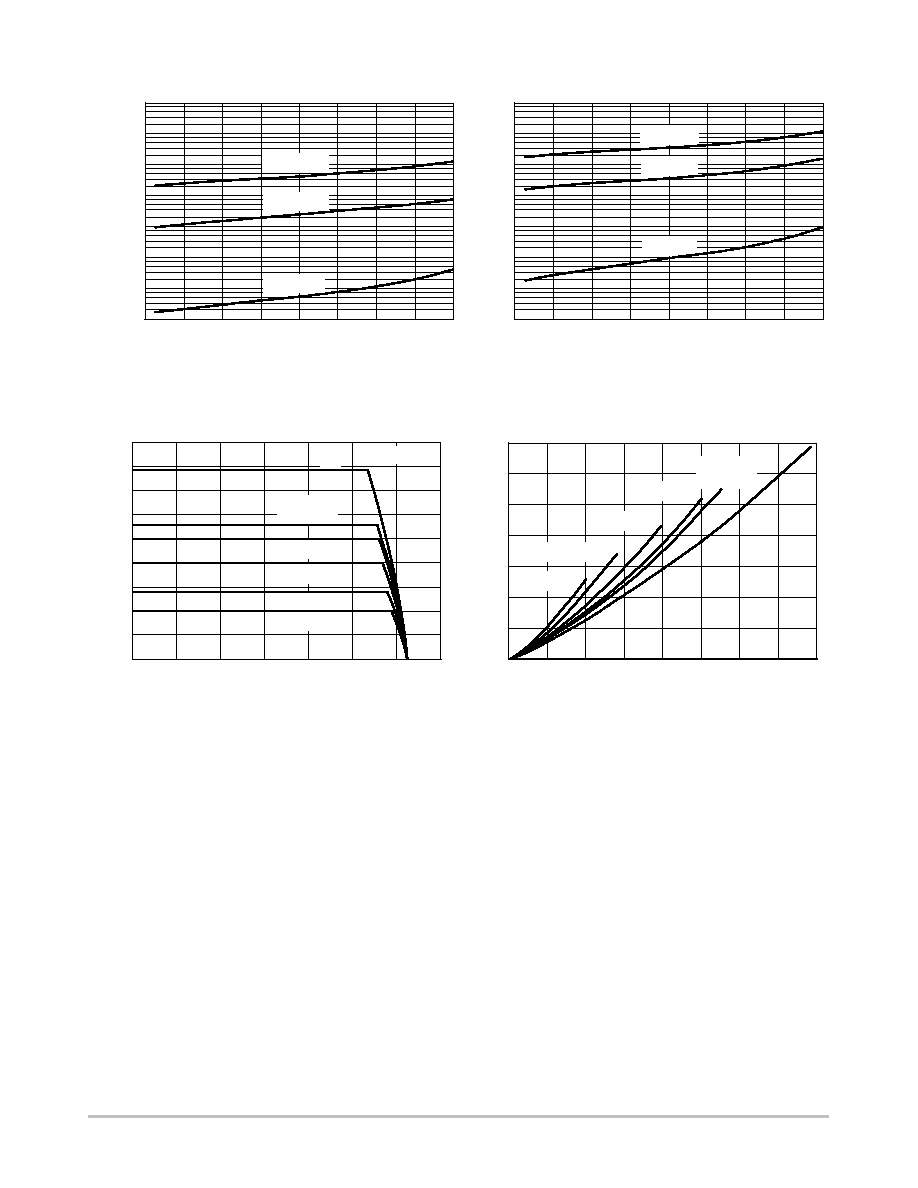
Figure 1. Typical Forward Voltage
Figure 2. Maximum Forward Voltage
0.2
v
F
, INSTANTANEOUS FORWARD VOLTAGE (VOLTS)
10
1.0
V
F
, MAXIMUM INSTANTANEOUS FORWARD VOLTAGE
(VOLTS)
0.1
0.6
0.4
0.8
T
J
= 100
∞
C
T
J
= 150
∞
C
T
J
= ≠40
∞
C
T
J
= 25
∞
C
0.2
10
1.0
0.1
0.6
0.4
0.8
T
J
= 100
∞
C
T
J
= 150
∞
C
T
J
= 25
∞
C
MBR120ESFT1
http://onsemi.com
3
V
R
, REVERSE VOLTAGE (VOLTS)
I
R
, MAXIMUM REVERSE CURRENT (AMPS)
I
R
, REVERSE CURRENT (AMPS)
Figure 3. Typical Reverse Current
Figure 4. Maximum Reverse Current
20
0
V
R
, REVERSE VOLTAGE (VOLTS)
100E≠3
10E≠3
10E≠6
1E≠6
100E≠9
10E≠9
5.0
10
15
20
0
100E≠3
10E≠3
1E≠3
100E≠9
10E≠9
5.0
10
15
T
J
= 150
∞
C
T
J
= 100
∞
C
T
J
= 25
∞
C
T
J
= 150
∞
C
T
J
= 100
∞
C
T
J
= 25
∞
C
100E≠6
10E≠6
1E≠6
100E≠6
1E≠3
Figure 5. Current Derating
Figure 6. Forward Power Dissipation
P
FO
, A
VERAGE DISSIP
A
TION (W
A
TTS)
I
pk
/I
o
= 5
I
O
, AVERAGE FORWARD CURRENT (AMPS)
0.2
0
0.7
0.6
0.5
0.3
0.1
0
1.0
0.4
0.8
1.2
1.6
0.4
SQUARE
WAVE
dc
I
pk
/I
o
=
p
I
pk
/I
o
= 10
I
pk
/I
o
= 20
0.6
1.4
0.2
I
O
, A
VERAGE FOR
W
ARD CURRENT (AMPS)
T
L
, LEAD TEMPERATURE (
∞
C)
45
25
1.8
1.2
1.0
0.6
0.2
0
85
105
165
0.8
65
125
0.4
1.4
1.6
I
pk
/I
o
= 20
I
pk
/I
o
= 10
I
pk
/I
o
= 5
I
pk
/I
o
=
p
SQUARE
WAVE
dc
freq = 20 kHz
145

MBR120ESFT1
http://onsemi.com
4
C, CAP
ACIT
ANCE (pF)
Figure 7. Capacitance
12
0
V
R
, REVERSE VOLTAGE (VOLTS)
1000
100
10
6.0
2.0
4.0
8.0
10
T
J
= 25
∞
C
20
18
16
14
Figure 8. Typical Operating Temperature
Derating*
* Reverse power dissipation and the possibility of thermal runaway must be considered when operating this device under any re-
verse voltage conditions. Calculations of T
J
therefore must include forward and reverse power effects. The allowable operating
T
J
may be calculated from the equation:
T
J
= T
Jmax
≠ r(t)(Pf + Pr) where
r(t) = thermal impedance under given conditions,
Pf = forward power dissipation, and
Pr = reverse power dissipation
This graph displays the derated allowable T
J
due to reverse bias under DC conditions only and is calculated as T
J
= T
Jmax
≠ r(t)Pr,
where r(t) = Rthja. For other power applications further calculations must be performed.
T
J
, DERA
TED OPERA
TING
TEMPERA
TURE (
∞
C)
12
0
V
R
, DC REVERSE VOLTAGE (VOLTS)
155
145
6.0
2.0
4.0
8.0
10
20
14
16
18
135
137
139
141
143
147
149
151
153
R
q
JA
= 25.6
∞
C/W
400
∞
C/W
324.9
∞
C/W
235
∞
C/W
130
∞
C/W
r(t), TRANSIENT THERMAL RESIST
ANCE
Figure 9. Thermal Response
1000
0.1
0.00001
t
1
, TIME (sec)
1000
1
0.0001
0.001
0.01
1
10
100
0.000001
0.1
10
100
P
(pk)
t
1
t
2
DUTY CYCLE, D = t
1
/t
2
q
JA = 321.8
∞
C/W
Test Type > Min Pad < Die Size 38x38 @ 75% mils
D = 0.5
SINGLE PULSE
0.2
0.1
0.05
0.01

MBR120ESFT1
http://onsemi.com
5
PACKAGE DIMENSIONS
SOD≠123LF
CASE 498≠01
ISSUE O
NOTES:
1. DIMENSIONING AND TOLERANCING PER ANSI
Y14.5M, 1982.
2. CONTROLLING DIMENSION: MILLIMETER.
3. DIMENSIONS A AND B DO NOT INCLUDE MOLD
FLASH.
4. DIMENSIONS D AND J ARE TO BE MEASURED
ON FLAT SECTION OF THE LEAD: BETWEEN 0.10
AND 0.25 MM FROM THE LEAD TIP.
DIM
MIN
MAX
MIN
MAX
INCHES
MILLIMETERS
A
1.50
1.80
0.059
0.071
B
2.50
2.90
0.098
0.114
C
0.90
1.00
0.039
D
0.70
1.10
0.028
0.043
E
0.55
0.95
0.022
0.037
H
0.00
0.10
0.000
0.004
J
0.10
0.20
0.004
0.008
K
3.40
3.80
0.134
0.150
L
0
8
∞
∞
0
8
∞
∞
0.035
A
B
K
D
C
H
E
L
J
L
POLARITY INDICATOR
OPTIONAL AS NEEDED