 | –≠–ª–µ–∫—Ç—Ä–æ–Ω–Ω—ã–π –∫–æ–º–ø–æ–Ω–µ–Ω—Ç: MBRM130L | –°–∫–∞—á–∞—Ç—å:  PDF PDF  ZIP ZIP |
©
Semiconductor Components Industries, LLC, 2002
December, 2002 - Rev. 1
1
Publication Order Number:
MBRM130L/D
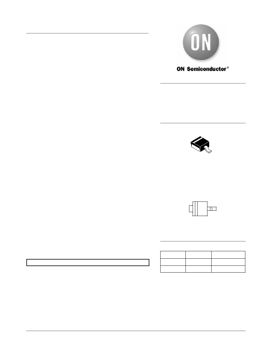
MBRM130L
Surface Mount
Schottky Power Rectifier
POWERMITE
Æ
Power Surface Mount Package
The Schottky Powermite employs the Schottky Barrier principle
with a barrier metal and epitaxial construction that produces optimal
forward voltage drop- reverse current tradeoff. The advanced
packaging techniques provide for a highly efficient micro miniature,
space saving surface mount Rectifier. With its unique heatsink design,
the Powermite has the same thermal performance as the SMA while
being 50% smaller in footprint area, and delivering one of the lowest
height profiles,
<
1.1 mm in the industry. Because of its small size, it is
ideal for use in portable and battery powered products such as cellular
and cordless phones, chargers, notebook computers, printers, PDAs
and PCMCIA cards. Typical applications are ac/dc and dc-dc
converters, reverse battery protection, and "Oring" of multiple supply
voltages and any other application where performance and size are
critical.
Features:
∑
Low Profile - Maximum Height of 1.1 mm
∑
Small Footprint - Footprint Area of 8.45 mm2
∑
Low V
F
Provides Higher Efficiency and Extends Battery Life
∑
Supplied in 12 mm Tape and Reel
∑
Low Thermal Resistance with Direct Thermal Path of Die on
Exposed Cathode Heat Sink
Mechanical Characteristics:
∑
Powermite is JEDEC Registered as DO-216AA
∑
Case: Molded Epoxy
∑
Epoxy Meets UL94V-0 at 1/8
∑
Weight: 62 mg (approximately)
∑
Device Marking: BCG
∑
Lead and Mounting Surface Temperature for Soldering Purposes.
260
∞
C Maximum for 10 Seconds
MAXIMUM RATINGS
Please See the Table on the Following Page
Device
Package
Shipping
ORDERING INFORMATION
MBRM130LT1
POWERMITE
3000/Tape & Reel
MBRM130LT3
POWERMITE 12,000/Tape & Reel
SCHOTTKY BARRIER
RECTIFIER
1.0 AMPERES
30 VOLTS
POWERMITE
CASE 457
PLASTIC
CATHODE
ANODE
MARKING DIAGRAM
M
BCG
BCG
= Device Code
M
= Date Code
http://onsemi.com

MBRM130L
http://onsemi.com
2
MAXIMUM RATINGS
Rating
Symbol
Value
Unit
Peak Repetitive Reverse Voltage
Working Peak Reverse Voltage
DC Blocking Voltage
V
RRM
V
RWM
V
R
30
V
Average Rectified Forward Current (At Rated V
R
, T
C
= 135
∞
C)
I
O
1.0
A
Peak Repetitive Forward Current
(At Rated V
R
, Square Wave, 100 kHz, T
C
= 135
∞
C)
I
FRM
2.0
A
Non-Repetitive Peak Surge Current
(Non-Repetitive peak surge current, halfwave, single phase, 60 Hz)
I
FSM
50
A
Storage Temperature
T
stg
-55 to 150
∞
C
Operating Junction Temperature
T
J
-55 to 125
∞
C
Voltage Rate of Change (Rated V
R
, T
J
= 25
∞
C)
dv/dt
10,000
V/
m
s
THERMAL CHARACTERISTICS
Thermal Resistance - Junction-to-Lead (Anode) (Note 1)
Thermal Resistance - Junction-to-Tab (Cathode) (Note 1)
Thermal Resistance - Junction-to-Ambient (Note 1)
R
tjl
R
tjtab
R
tja
35
23
277
∞
C/W
1. Mounted with minimum recommended pad size, PC Board FR4, See Figures 9 & 10.
ELECTRICAL CHARACTERISTICS
Maximum Instantaneous Forward Voltage (Note 2), See Figure 2
V
F
T
J
= 25
∞
C
T
J
= 85
∞
C
V
(I
F
= 0.1 A)
(I
F
= 1.0 A)
(I
F
= 3.0 A)
0.30
0.38
0.52
0.20
0.33
0.50
Maximum Instantaneous Reverse Current (Note 2), See Figure 4
I
R
T
J
= 25
∞
C
T
J
= 85
∞
C
mA
(V
R
= 30 V)
(V
R
= 20 V)
(V
R
= 10 V)
0.41
0.13
0.05
11
5.3
3.2
2. Pulse Test: Pulse Width
250
µ
s, Duty Cycle
2%.

MBRM130L
http://onsemi.com
3
I
R
, MAXIMUM REVERSE CURRENT (AMPS)
I
R
, REVERSE CURRENT (AMPS)
I
F
, INST
ANT
ANEOUS FOR
W
ARD CURRENT (AMPS)
i
F
, INST
ANT
ANEOUS FOR
W
ARD CURRENT (AMPS)
Figure 1. Typical Forward Voltage
Figure 2. Maximum Forward Voltage
Figure 3. Typical Reverse Current
Figure 4. Maximum Reverse Current
0
v
F
, INSTANTANEOUS FORWARD VOLTAGE (VOLTS)
10
1.0
V
F
, MAXIMUM INSTANTANEOUS FORWARD VOLTAGE
(VOLTS)
20
0
V
R
, REVERSE VOLTAGE (VOLTS)
10E-3
1.0E-3
100E-6
10E-6
1.0E-6
V
R
, REVERSE VOLTAGE (VOLTS)
0.1
0.3
0.1
0.2
0.4
5.0
10
15
30
0
100E-6
10E-6
5.0
10
15
T
J
= 85
∞
C
T
J
= 125
∞
C
T
J
= -40
∞
C
T
J
= 25
∞
C
T
J
= 85
∞
C
T
J
= 25
∞
C
10
1.0
0.1
100E-3
10E-3
1.0E-3
30
25
20
25
0.6
T
J
= 125
∞
C
0.5
0
0.3
0.1
0.2
0.4
T
J
= 85
∞
C
T
J
= 125
∞
C
T
J
= -40
∞
C
T
J
= 25
∞
C
0.6
T
J
= 125
∞
C
0.5
T
J
= 85
∞
C
T
J
= 25
∞
C

MBRM130L
http://onsemi.com
4
P
FO
, A
VERAGE POWER DISSIP
A
TION (W
A
TTS)
I
O
, A
VERAGE FOR
W
ARD CURRENT (AMPS)
I
pk
/I
o
= 5
Figure 5. Current Derating
Figure 6. Forward Power Dissipation
45
75
25
T
L
, LEAD TEMPERATURE (
∞
C)
1.8
1.2
1.0
0.8
0.2
0
I
O
, AVERAGE FORWARD CURRENT (AMPS)
0.2
0
0.7
0.6
0.5
0.3
0.1
0
1.0
55
115
105
1.4
0.4
0.8
1.2
1.6
0.4
125
1.6
SQUARE
WAVE
dc
I
pk
/I
o
=
p
I
pk
/I
o
= 10
I
pk
/I
o
= 20
I
pk
/I
o
= 20
I
pk
/I
o
= 10
I
pk
/I
o
= 5
I
pk
/I
o
=
p
SQUARE WAVE
dc
0.6
0.4
FREQ = 20 kHz
0.6
1.4
0.2
35
65
85
95
T
J
, DERA
TED OPERA
TING TEMPERA
TURE (
_
C)
C, CAP
ACIT
ANCE (pF)
Figure 7. Capacitance
Figure 8. Typical Operating Temperature Derating*
0
V
R
, REVERSE VOLTAGE (VOLTS)
1000
100
10
V
R
, DC REVERSE VOLTAGE (VOLTS)
15
30
0
60
40
20
10
5.0
15
20
5.0
10
50
140
150
* Reverse power dissipation and the possibility of thermal runaway must be considered when operating this device under any re-
verse voltage conditions. Calculations of T
J
therefore must include forward and reverse power effects. The allowable operating
T
J
may be calculated from the equation:
T
J
= T
Jmax
- r(t)(Pf + Pr) where
r(t) = thermal impedance under given conditions,
Pf = forward power dissipation, and
Pr = reverse power dissipation
This graph displays the derated allowable T
J
due to reverse bias under DC conditions only and is calculated as T
J
= T
Jmax
- r(t)Pr,
where r(t) = Rthja. For other power applications further calculations must be performed.
R
tja
= 10
∞
C/W
15
∞
C/W
25
∞
C/W
35
∞
C/W
T
J
= 25
∞
C
30
20
25
80
25
20
∞
C/W
30
120
100
110
130
90
70

MBRM130L
http://onsemi.com
5
R
(T)
, TRANSIENT THERMAL RESIST
ANCE (NORMALIZED)
R
(T)
, TRANSIENT THERMAL RESIST
ANCE (NORMALIZED)
T, TIME (s)
1.0
0.1
0.01
0.001
100
0.1
0.00001
1,000
0.0001
0.001
0.01
1.0
10
Rtjl(t) = Rtjl*r(t)
50%
20%
10%
5.0%
2.0%
1.0%
Figure 9. Thermal Response Junction to Lead
100
0.1
0.00001
T, TIME (s)
1.0
0.1
0.01
0.0001
0.001
0.01
1.0
10
0.001
Rtjl(t) = Rtjl*r(t)
50%
20%
10%
5.0%
2.0%
1.0%
Figure 10. Thermal Response Junction to Ambient
Minimum Recommended Footprint
0.100
2.54
0.025
0.635
0.050
1.27
0.105
2.67
0.030
0.762
inches
mm