©
Semiconductor Components Industries, LLC, 2002
April, 2002 ≠ Rev. 4
1
Publication Order Number:
MC10E212/D
MC10E212, MC100E212
5V ECL 3 Bit Scannable
Registered Address Driver
The MC10E/100E212 is a scannable registered ECL driver typically
used as a fan-out memory address driver for ECL cache driving. In a
VLSI array based CPU design, use of the E212 allows the user to
conserve array output cell functionality and also output pins.
The input shift register is designed with control logic which greatly
facilitates its use in boundary scan applications.
The 100 Series contains temperature compensation.
∑
Scannable Version E112 Driver
∑
1025 ps Max. CLK to Output
∑
Dual Differential Outputs
∑
Master Reset
∑
PECL Mode Operating Range: VCC= 4.2 V to 5.7 V
with VEE= 0 V
∑
NECL Mode Operating Range: VCC= 0 V
with VEE= ≠4.2 V to ≠5.7 V
∑
Internal Input Pulldown Resistors
∑
ESD Protection: > 1 KV HBM, > 75 V MM
∑
Meets or Exceeds JEDEC Spec EIA/JESD78 IC Latchup Test
∑
Moisture Sensitivity Level 1
For Additional Information, see Application Note AND8003/D
∑
Flammability Rating: UL≠94 code V≠0 @ 1/8",
Oxygen Index 28 to 34
∑
Transistor Count = 259 devices
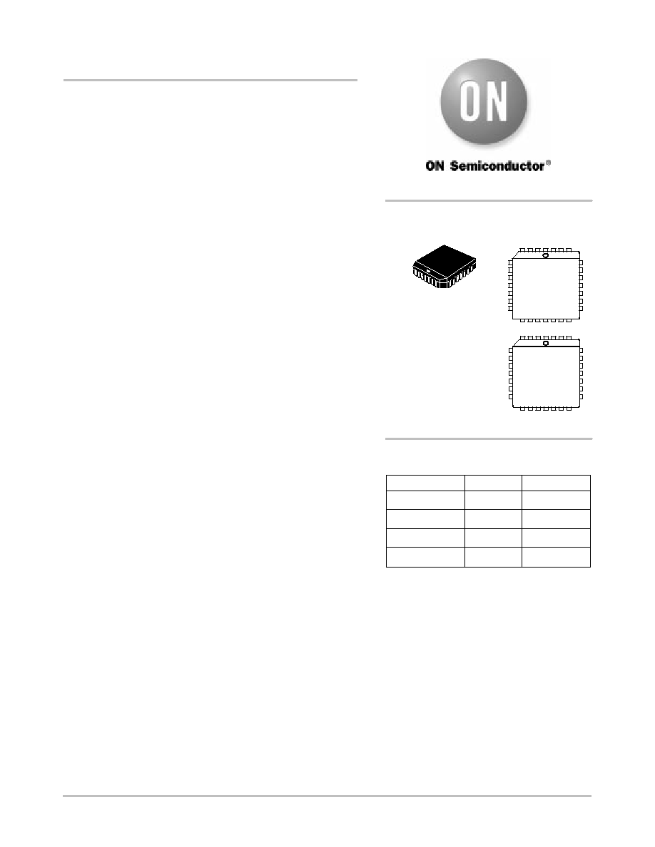
Device
Package
Shipping
ORDERING INFORMATION
MC10E212FN
PLCC≠28
37 Units/Rail
MC10E212FNR2
PLCC≠28
500 Units/Reel
MC100E212FN
PLCC≠28
37 Units/Rail
MC100E212FNR2
PLCC≠28
500 Units/Reel
MARKING
DIAGRAMS
A
= Assembly Location
WL = Wafer Lot
YY = Year
WW = Work Week
PLCC≠28
FN SUFFIX
CASE 776
MC10E212FN
AWLYYWW
MC100E212FN
AWLYYWW
http://onsemi.com
1 28
1 28

LOGIC DIAGRAM
D2
D1
D0
S-IN
LOAD
SHIFT
CLK
MR
D
Q
D
D
Q
Q
S OUT
Q2b
Q2a
Q2b
Q2a
Q1b
Q1a
Q1b
Q1a
Q0b
Q0a
Q0b
Q0a
1
0
1
0
1
0
1
0
1
0
1
0
MC10E212, MC100E212
http://onsemi.com
2
5
25
24
23
22
21
20
19
18
17
16
15
14
13
12
5
6
7
8
9
10
11
26
27
28
2
3
4
SHIFT MR NC S-OUT VCCOQ2b Q2a
Q2b
Q2a
VCC
Q1b
Q1a
Q1b
Q1a
NC VCCOQ0a
LOAD
CLK
D2
VEE
D1
D0
S-IN
Q0b Q0a Q0b VCCO
1
Pinout: 28-Lead PLCC
(Top View)
* All VCC and VCCO pins are tied together on the die.
LOGIC DIAGRAM AND PINOUT ASSIGNMENT
Warning: All VCC, VCCO, and VEE pins must be externally
connected to Power Supply to guarantee proper operation.
PIN DESCRIPTION
PIN
FUNCTION
D0 ≠ D2
ECL Data Inputs
S-IN
ECL Scan Input
LOAD
ECL LOAD/HOLD Control
SHIFT
ECL Scan Control
CLK
ECL Clock
MR
ECL Reset
S-OUT
ECL Scan Output
Q[0:2]a, Q[0:2]b
ECL True Outputs
Q[0:2]a, Q[0:2]b
ECL Inverting Outputs
VCC, VCCO
Positive Supply
VEE
Negative Supply
NC
No Connect
FUNCTION TABLE
LOAD
SHIFT
MR
MODE
L
L
L
Load
H
L
L
Hold
X
H
L
Shift
X
X
H
Reset

MC10E212, MC100E212
http://onsemi.com
3
MAXIMUM RATINGS
(Note 1)
Symbol
Parameter
Condition 1
Condition 2
Rating
Units
VCC
PECL Mode Power Supply
VEE = 0 V
8
V
VEE
NECL Mode Power Supply
VCC = 0 V
≠8
V
VI
PECL Mode Input Voltage
VEE = 0 V
VI
VCC
6
V
I
C
ode
u
o age
NECL Mode Input Voltage
EE
0
VCC = 0 V
I
CC
VI
VEE
6
≠6
V
Iout
Output Current
Continuous
Surge
50
100
mA
mA
TA
Operating Temperature Range
0 to +85
∞
C
Tstg
Storage Temperature Range
≠65 to +150
∞
C
JA
Thermal Resistance (Junction to Ambient)
0 LFPM
500 LFPM
28 PLCC
28 PLCC
63.5
43.5
∞
C/W
∞
C/W
JC
Thermal Resistance (Junction to Case)
std bd
28 PLCC
22 to 26
∞
C/W
VEE
PECL Operating Range
NECL Operating Range
4.2 to 5.7
≠5.7 to ≠4.2
V
V
Tsol
Wave Solder
<2 to 3 sec @ 248
∞
C
265
∞
C
1. Maximum Ratings are those values beyond which device damage may occur.
10E SERIES PECL DC CHARACTERISTICS
VCCx= 5.0 V; VEE= 0.0 V (Note 1)
0
∞
C
25
∞
C
85
∞
C
Symbol
Characteristic
Min
Typ
Max
Min
Typ
Max
Min
Typ
Max
Unit
IEE
Power Supply Current
80
96
80
96
80
96
mA
VOH
Output HIGH Voltage (Note 2)
3980
4070
4160
4020
4105
4190
4090
4185
4280
mV
VOL
Output LOW Voltage (Note 2)
3050
3210
3370
3050
3210
3370
3050
3227
3405
mV
VIH
Input HIGH Voltage
3830
3995
4160
3870
4030
4190
3940
4110
4280
mV
VIL
Input LOW Voltage
3050
3285
3520
3050
3285
3520
3050
3302
3555
mV
IIH
Input HIGH Current
150
150
150
µ
A
IIL
Input LOW Current
0.5
0.3
0.5
0.25
0.3
0.2
µ
A
NOTE: Devices are designed to meet the DC specifications shown in the above table, after thermal equilibrium has been established. The
circuit is in a test socket or mounted on a printed circuit board and transverse air flow greater than 500 lfpm is maintained.
1. Input and output parameters vary 1:1 with VCC. VEE can vary +0.46 V / ≠0.06 V.
2. Outputs are terminated through a 50 ohm resistor to VCC≠2 volts.
10E SERIES NECL DC CHARACTERISTICS
VCCx= 0.0 V; VEE= ≠5.0 V (Note 1)
0
∞
C
25
∞
C
85
∞
C
Symbol
Characteristic
Min
Typ
Max
Min
Typ
Max
Min
Typ
Max
Unit
IEE
Power Supply Current
80
96
80
96
80
96
mA
VOH
Output HIGH Voltage (Note 2)
≠1020
≠930
≠840
≠980
≠895
≠810
≠910
≠815
≠720
mV
VOL
Output LOW Voltage (Note 2)
≠1950
≠1790
≠1630
≠1950
≠1790
≠1630
≠1950
≠1773
≠1595
mV
VIH
Input HIGH Voltage
≠1170
≠1005
≠840
≠1130
≠970
≠810
≠1060
≠890
≠720
mV
VIL
Input LOW Voltage
≠1950
≠1715
≠1480
≠1950
≠1715
≠1480
≠1950
≠1698
≠1445
mV
IIH
Input HIGH Current
150
150
150
µ
A
IIL
Input LOW Current
0.5
0.3
0.5
0.065
0.3
0.2
µ
A
NOTE: Devices are designed to meet the DC specifications shown in the above table, after thermal equilibrium has been established. The
circuit is in a test socket or mounted on a printed circuit board and transverse air flow greater than 500 lfpm is maintained.
1. Input and output parameters vary 1:1 with VCC. VEE can vary +0.46 V / ≠0.06 V.
2. Outputs are terminated through a 50 ohm resistor to VCC≠2 volts.

MC10E212, MC100E212
http://onsemi.com
4
100E SERIES PECL DC CHARACTERISTICS
VCCx= 5.0 V; VEE= 0.0 V (Note 1)
0
∞
C
25
∞
C
85
∞
C
Symbol
Characteristic
Min
Typ
Max
Min
Typ
Max
Min
Typ
Max
Unit
IEE
Power Supply Current
80
96
80
96
92
110
mA
VOH
Output HIGH Voltage (Note 2)
3975
4050
4120
3975
4050
4120
3975
4050
4120
mV
VOL
Output LOW Voltage (Note 2)
3190
3295
3380
3190
3255
3380
3190
3260
3380
mV
VIH
Input HIGH Voltage
3835
4050
4120
3835
4120
4120
3835
4120
4120
mV
VIL
Input LOW Voltage
3190
3300
3525
3190
3525
3525
3190
3525
3525
mV
IIH
Input HIGH Current
150
150
150
µ
A
IIL
Input LOW Current
0.5
0.3
0.5
0.25
0.5
0.2
µ
A
NOTE: Devices are designed to meet the DC specifications shown in the above table, after thermal equilibrium has been established. The
circuit is in a test socket or mounted on a printed circuit board and transverse air flow greater than 500 lfpm is maintained.
1. Input and output parameters vary 1:1 with VCC. VEE can vary +0.4 6V / ≠0.8 V.
2. Outputs are terminated through a 50 ohm resistor to VCC≠2 volts.
100E SERIES NECL DC CHARACTERISTICS
VCCx= 0.0 V; VEE= ≠5.0 V (Note 1)
0
∞
C
25
∞
C
85
∞
C
Symbol
Characteristic
Min
Typ
Max
Min
Typ
Max
Min
Typ
Max
Unit
IEE
Power Supply Current
80
96
80
96
92
110
mA
VOH
Output HIGH Voltage (Note 2)
≠1025
≠950
≠880
≠1025
≠950
≠880
≠1025
≠950
≠880
mV
VOL
Output LOW Voltage (Note 2)
≠1810
≠1705
≠1620
≠1810
≠1745
≠1620
≠1810
≠1740
≠1620
mV
VIH
Input HIGH Voltage
≠1165
≠950
≠880
≠1165
≠880
≠880
≠1165
≠880
≠880
mV
VIL
Input LOW Voltage
≠1810
≠1700
≠1475
≠1810
≠1475
≠1475
≠1810
≠1475
≠1475
mV
IIH
Input HIGH Current
150
150
150
µ
A
IIL
Input LOW Current
0.5
0.3
0.5
0.25
0.5
0.2
µ
A
NOTE: Devices are designed to meet the DC specifications shown in the above table, after thermal equilibrium has been established. The
circuit is in a test socket or mounted on a printed circuit board and transverse air flow greater than 500 lfpm is maintained.
1. Input and output parameters vary 1:1 with VCC. VEE can vary +0.46 V / ≠0.8 V.
2. Outputs are terminated through a 50 ohm resistor to VCC≠2 volts.
AC CHARACTERISTICS
VCCx= 5.0 V; VEE= 0.0 V or VCCx= 0.0 V; VEE= ≠5.0 V (Note 1)
0
∞
C
25
∞
C
85
∞
C
Symbol
Characteristic
Min
Typ
Max
Min
Typ
Max
Min
Typ
Max
Unit
fMAX
Maximum Toggle Frequency
TBD
TBD
TBD
GHz
tPLH
Propagation Delay to Output
ps
tPHL
CLK
575
800
1025
575
800
1025
575
800
1025
MR
575
800
1025
575
800
1025
575
800
1025
CLK to S-OUT
575
800
1025
575
800
1025
575
800
1025
ts
Setup Time
ps
D
175
25
175
25
175
25
SHIFT
150
≠ 50
150
≠ 50
150
≠ 50
LOAD
225
50
225
50
225
50
S-IN
150
≠ 50
150
≠ 50
150
≠ 50
th
Hold Time
ps
D
250
25
250
25
250
25
SHIFT
300
100
300
100
300
100
LOAD
225
0
225
0
225
0
S-IN
300
100
300
100
300
100
tRR
Reset Recovery
600
350
600
350
600
350
ps
tSKEW
Within-Device Skew (Note 1.)
100
100
100
ps
tSKEW
Within-Gate Skew (Note 2.)
50
50
50
ps
tJITTER
Cycle≠to≠Cycle Jitter
TBD
TBD
TBD
ps
tr
Rise/Fall Times
ps
tf
(20 - 80%)
275
425
650
275
425
650
275
425
650
1. 10 Series: VEE can vary +0.46 V / ≠0.06 V.
100 Series: VEE can vary +0.46 V / ≠0.8 V.
1. Within-device skew is defined as identical transitions on similar paths through a device.

MC10E212, MC100E212
http://onsemi.com
5
2. Within-gate skew is defined as the difference in delays between various outputs of a gate when driven from the same input.
Figure 1. Typical Termination for Output Driver and Device Evaluation
(See Application Note AND8020 ≠ Termination of ECL Logic Devices.)
W
Driver
Device
Receiver
Device
Q
D
50
W
50
V TT
Q
D
VTT = VCC ≠ 2.0 V
Resource Reference of Application Notes
AN1404
≠
ECLinPS Circuit Performance at Non≠Standard VIH Levels
AN1405
≠
ECL Clock Distribution Techniques
AN1406
≠
Designing with PECL (ECL at +5.0 V)
AN1503
≠
ECLinPS I/O SPICE Modeling Kit
AN1504
≠
Metastability and the ECLinPS Family
AN1568
≠
Interfacing Between LVDS and ECL
AN1596
≠
ECLinPS Lite Translator ELT Family SPICE I/O Model Kit
AN1650
≠
Using Wire≠OR Ties in ECLinPS Designs
AN1672
≠
The ECL Translator Guide
AND8001
≠
Odd Number Counters Design
AND8002
≠
Marking and Date Codes
AND8020
≠
Termination of ECL Logic Devices