⌐
Semiconductor Components Industries, LLC, 2001
April, 2001 ¡ Rev. 1
1
Publication Order Number:
MC100EP16F/D
MC100EP16F
3.3V / 5V ECL Differential
Receiver/Driver With
Reduced Output Swing
The MC100EP16F is a differential receiver/driver. The device is
functionally equivalent to the EP16 device with higher performance
capabilities. With reduced output swings, rise/fall transition times are
significantly faster than on the EP16. The EP16F is ideally suited for
interfacing with high frequency sources.
The V
BB
pin, an internally generated voltage supply, is available to
this device only. For single¡ended input conditions, the unused
differential input is connected to V
BB
as a switching reference voltage.
V
BB
may also rebias AC coupled inputs. When used, decouple V
BB
and V
CC
via a 0.01
mF capacitor and limit current sourcing or sinking
to 0.5 mA. When not used, V
BB
should be left open.
╖
100 ps Typical Rise and Fall Time
╖
Max Frequency >4 GHz Typical
╖
The 100 Series Contains Temperature Compensation
╖
PECL Mode Operating Range: V
CC
=
3.0 V to 5.5 V
with V
EE
= 0 V
╖
NECL Mode Operating Range: V
CC
=
0V
with V
EE
= ¡3.0 V to ¡5.5 V
╖
Open Input Default State
╖
Safety Clamp on Inputs
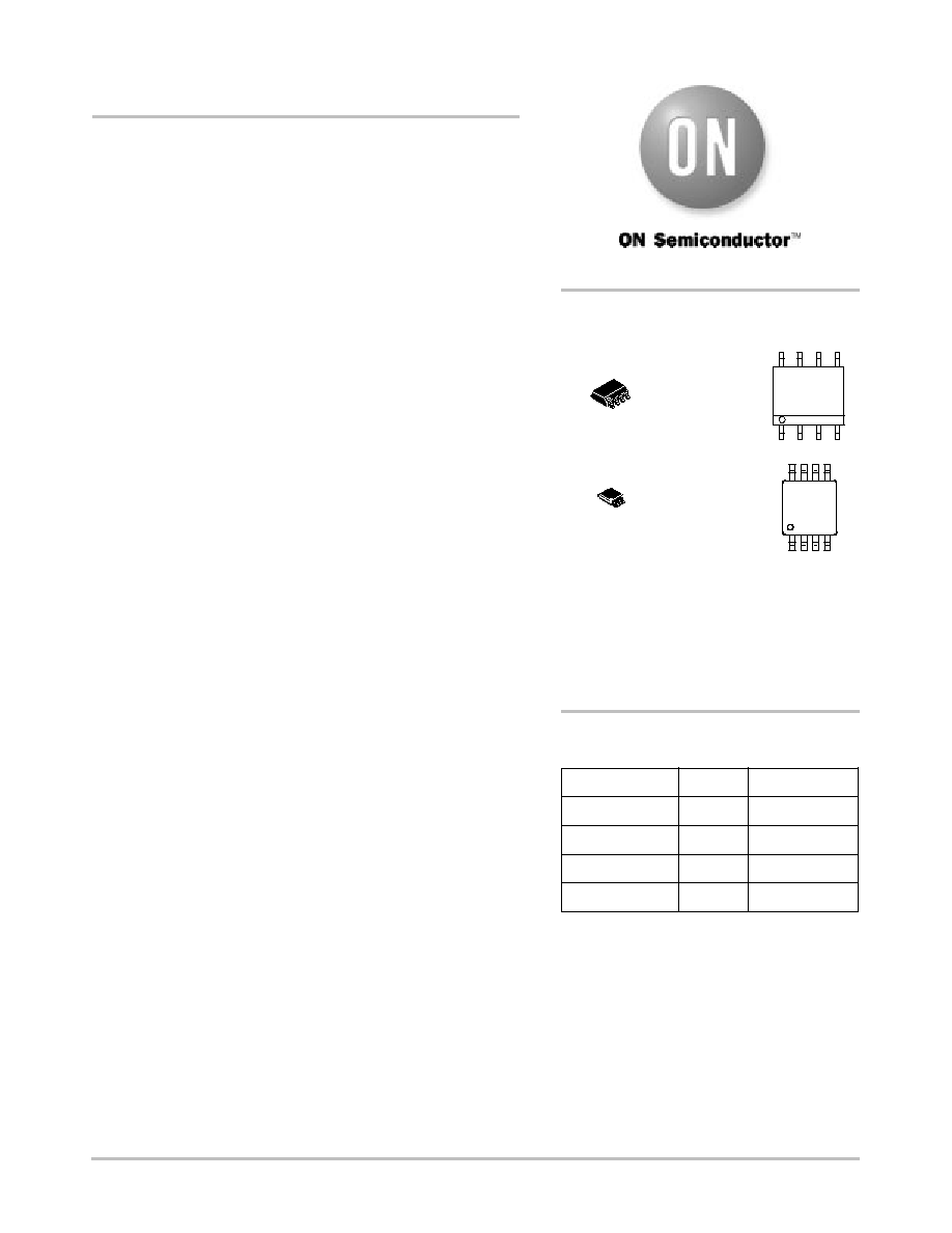
MC100EP16FDT
Device
Package
Shipping
ORDERING INFORMATION
MC100EP16FD
SO¡8
98 Units/Rail
MC100EP16FDR2
SO¡8
2500 Tape & Reel
TSSOP¡8
100 Units/Rail
MC100EP16FDTR2
TSSOP¡8 2500 Tape & Reel
http://onsemi.com
A = Assembly Location
L = Wafer Lot
Y = Year
W = Work Week
*For additional information, see Application Note
AND8002/D
SO¡8
D SUFFIX
CASE 751
TSSOP¡8
DT SUFFIX
CASE 948R
1
8
1
8
ALYW
HKP60
1
KEP60
1
8
ALYW
8
MARKING
DIAGRAMS*

MC100EP16F
http://onsemi.com
2
1
2
3
4
5
6
7
8
Q
V
EE
V
CC
Figure 1. 8¡Lead Pinout (Top View) and Logic Diagram
D
Q
D
V
BB
NC
Q, Q
ECL Data Outputs
ECL Data Inputs
V
BB
Reference Voltage Output
PIN DESCRIPTION
PIN
D*, D**
FUNCTION
V
CC
Positive Supply
V
EE
Negative Supply
NC
No Connect
* Pins will default LOW when left open.
** Pins will default to V
CC
/2 when left open.
ATTRIBUTES
Characteristics
Value
Internal Input Pulldown Resistor
75 k
W
Internal Input Pullup Resistor
37.5 k
W
ESD Protection
Human Body Model
Machine Model
Charged Device Model
> 4 kV
> 200 V
> 2 kV
Moisture Sensitivity, Indefinite Time Out of Drypack (Note 1.)
Level 1
Flammability Rating
Oxygen Index
UL¡94 code V¡0 A 1/8"
28 to 34
Transistor Count
139
Meets or exceeds JEDEC Spec EIA/JESD78 IC Latchup Test
1. For additional information, see Application Note AND8003/D.
MAXIMUM RATINGS
(Note 2.)
Symbol
Parameter
Condition 1
Condition 2
Rating
Units
V
CC
PECL Mode Power Supply
V
EE
= 0 V
6
V
V
EE
NECL Mode Power Supply
V
CC
= 0 V
¡6
V
V
I
PECL Mode Input Voltage
V
EE
= 0 V
V
I
V
CC
6
V
I
C
ode
u
o age
NECL Mode Input Voltage
EE
0
V
CC
= 0 V
I
CC
V
I
V
EE
6
¡6
V
I
out
Output Current
Continuous
Surge
50
100
mA
mA
I
BB
V
BB
Sink/Source
▒
0.5
mA
TA
Operating Temperature Range
¡40 to +85
░
C
T
stg
Storage Temperature Range
¡65 to +150
░
C
JA
Thermal Resistance (Junction to Ambient)
0 LFPM
500 LFPM
8 SOIC
8 SOIC
190
130
░
C/W
░
C/W
JC
Thermal Resistance (Junction to Case)
std bd
8 SOIC
41 to 44
▒
5%
░
C/W
JA
Thermal Resistance (Junction to Ambient)
0 LFPM
500 LFPM
8 TSSOP
8 TSSOP
185
140
░
C/W
░
C/W
JC
Thermal Resistance (Junction to Case)
std bd
8 TSSOP
41 to 44
▒
5%
░
C/W
T
sol
Wave Solder
<2 to 3 sec @ 248
░
C
265
░
C
2. Maximum Ratings are those values beyond which device damage may occur.

MC100EP16F
http://onsemi.com
3
DC CHARACTERISTICS, PECL
V
CC
= 3.3 V, V
EE
= 0 V (Note 3.)
¡40
░
C
25
░
C
85
░
C
Symbol
Characteristic
Min
Typ
Max
Min
Typ
Max
Min
Typ
Max
Unit
IEE
Power Supply Current
23
28
35
25
31
38
26
33
40
mA
V
OH
Output HIGH Voltage (Note 4.)
2155
2280
2405
2155
2280
2405
2155
2280
2405
mV
V
OL
Output LOW Voltage (Note 4.)
1575
1690
1775
1575
1690
1775
1575
1690
1775
mV
V
IH
Input HIGH Voltage (Single Ended)
2075
2420
2075
2420
2075
2420
mV
V
IL
Input LOW Voltage (Single Ended)
(Note 5.)
1490
1675
1490
1675
1490
1675
mV
V
BB
Output Voltage Reference
1775
1875
1975
1775
1875
1975
1775
1875
1975
mV
V
IHCMR
Input HIGH Voltage Common Mode
Range (Differential) (Note 6.)
2.0
3.3
2.0
3.3
2.0
3.3
V
I
IH
Input HIGH Current
150
150
150
╡
A
I
IL
Input LOW Current
D
D
0.5
¡150
0.5
¡150
0.5
¡150
╡
A
NOTE: EP circuits are designed to meet the DC specifications shown in the above table after thermal equilibrium has been established. The
circuit is in a test socket or mounted on a printed circuit board and transverse airflow greater than 500 lfpm is maintained.
3. Input and output parameters vary 1:1 with V
CC
. V
EE
can vary +0.3 V to ¡2.2 V.
4. All loading with 50 ohms to V
CC
¡2.0 volts.
5. Not recommended for single ended operation when using an EP16F to drive another EP16F. V
OL
has reduced output swing and may not
meet the V
IL
specification over temperature.
6. V
IHCMR
min varies 1:1 with V
EE
, V
IHCMR
max varies 1:1 with V
CC
. The V
IHCMR
range is referenced to the most positive side of the differential
input signal.
DC CHARACTERISTICS, PECL
V
CC
= 5.0 V, V
EE
= 0 V (Note 7.)
¡40
░
C
25
░
C
85
░
C
Symbol
Characteristic
Min
Typ
Max
Min
Typ
Max
Min
Typ
Max
Unit
IEE
Power Supply Current
23
28
35
25
31
38
26
33
40
mA
V
OH
Output HIGH Voltage (Note 8.)
3855
3980
4105
3855
3980
4105
3855
3980
4105
mV
V
OL
Output LOW Voltage (Note 8.)
3275
3390
3475
3275
3390
3475
3275
3390
3475
mV
V
IH
Input HIGH Voltage (Single Ended)
3775
4120
3775
4120
3775
4120
mV
V
IL
Input LOW Voltage (Single Ended)
(Note 9.)
3190
3375
3190
3375
3190
3375
mV
V
BB
Output Voltage Reference
3475
3575
3675
3475
3575
3675
3475
3575
3675
mV
V
IHCMR
Input HIGH Voltage Common Mode
Range (Differential) (Note 10.)
2.0
5.0
2.0
5.0
2.0
5.0
V
I
IH
Input HIGH Current
150
150
150
╡
A
I
IL
Input LOW Current
D
D
0.5
¡150
0.5
¡150
0.5
¡150
╡
A
NOTE: EP circuits are designed to meet the DC specifications shown in the above table after thermal equilibrium has been established. The
circuit is in a test socket or mounted on a printed circuit board and transverse airflow greater than 500 lfpm is maintained.
7. Input and output parameters vary 1:1 with V
CC
. V
EE
can vary +2.0 V to ¡0.5 V.
8. All loading with 50 ohms to V
CC
¡2.0 volts.
9. Not recommended for single ended operation when using an EP16F to drive another EP16F. V
OL
has reduced output swing and may not
meet the V
IL
specification over temperature.
10. V
IHCMR
min varies 1:1 with V
EE
, V
IHCMR
max varies 1:1 with V
CC
. The V
IHCMR
range is referenced to the most positive side of the differential
input signal.

MC100EP16F
http://onsemi.com
4
DC CHARACTERISTICS, NECL
V
CC
= 0V; V
EE
= ¡5.5V to ¡3.0V (Note 11.)
¡40
░
C
25
░
C
85
░
C
Symbol
Characteristic
Min
Typ
Max
Min
Typ
Max
Min
Typ
Max
Unit
IEE
Power Supply Current
23
28
35
25
31
38
26
33
40
mA
V
OH
Output HIGH Voltage (Note 12.)
¡1145
¡1020
¡895
¡1145
¡1020
¡895
¡1145
¡1020
¡895
mV
V
OL
Output LOW Voltage (Note 12.)
¡1725
¡1610
¡1525
¡1725
¡1610
¡1525
¡1725
¡1610
¡1525
mV
V
IH
Input HIGH Voltage (Single Ended)
¡1225
¡880
¡1225
¡880
¡1225
¡880
mV
V
IL
Input LOW Voltage (Single Ended)
(Note 13.)
¡1810
¡1625
¡1810
¡1625
¡1810
¡1625
mV
V
BB
Output Voltage Reference
¡1525
¡1425
¡1325
¡1525
¡1425
¡1325
¡1525
¡1425
¡1325
mV
V
IHCMR
Input HIGH Voltage Common Mode
Range (Differential) (Note 14.)
V
EE
+2.0
0.0
V
EE
+2.0
0.0
V
EE
+2.0
0.0
V
I
IH
Input HIGH Current
150
150
150
╡
A
I
IL
Input LOW Current
D
D
0.5
¡150
0.5
¡150
0.5
¡150
╡
A
NOTE: EP circuits are designed to meet the DC specifications shown in the above table after thermal equilibrium has been established. The
circuit is in a test socket or mounted on a printed circuit board and transverse airflow greater than 500 lfpm is maintained.
11. Input and output parameters vary 1:1 with V
CC
.
12. All loading with 50 ohms to V
CC
¡2.0 volts.
13. Not recommended for single ended operation when using an EP16F to drive another EP16F. V
OL
has reduced output swing and may not
meet the V
IL
specification over temperature.
14. V
IHCMR
min varies 1:1 with V
EE
, V
IHCMR
max varies 1:1 with V
CC
. The V
IHCMR
range is referenced to the most positive side of the differential
input signal.
AC CHARACTERISTICS
V
CC
= 0V; V
EE
= ¡3.0V to ¡5.5V or V
CC
= 3.0V to 5.5V; V
EE
=
0V (Note 15.)
¡40
░
C
25
░
C
85
░
C
Symbol
Characteristic
Min
Typ
Max
Min
Typ
Max
Min
Typ
Max
Unit
f
max
Maximum Toggle Frequency
(See Figure 2. F
max
/JITTER)
> 4
> 4
> 4
GHz
t
PLH
,
t
PHL
Propagation Delay to Output Differen-
tial
170
210
250
180
220
260
200
250
300
ps
t
SKEW
Duty Cycle Skew
5.0
20
5.0
20
5.0
20
ps
t
JITTER
Cycle¡to¡Cycle Jitter (RMS)
(See Figure 2. F
max
/JITTER)
0.2
< 1
0.2
< 1
0.2
< 1
ps
V
PP
Input Voltage Swing (Differential)
150
800
1200
150
800
1200
150
800
1200
mV
t
r
t
f
Output Rise/Fall Times
Q
(20% ¡ 80%)
70
85
110
80
100
120
90
110
130
ps
15. Measured using a 750 mV source, 50% duty cycle clock source. All loading with 50 ohms to V
CC
¡2.0 V.

MC100EP16F
http://onsemi.com
5
0
100
200
300
400
500
600
700
800
0
1000
2000
3000
4000
5000
6000
Figure 2. F
max/JITTER
FREQUENCY (MHz)
Measured
Simulated
1
2
3
4
5
6
7
8
(JITTER)
╔╔╔╔╔╔╔╔
╔╔╔╔╔╔╔╔
╔╔╔╔╔╔╔╔
V
OUTpp
(mV)
JITTER
OUT
ps (RMS)
╔
╔
V TT = V CC ¡ 2.0 V
Figure 3. Typical Termination for Output Driver and Device Evaluation
(See Application Note AND8020 ¡ Termination of ECL Logic Devices.)
W
Driver
Device
Receiver
Device
Q
Qb
D
Db
50
W
50
V TT
Resource Reference of Application Notes
AN1404
¡
ECLinPS Circuit Performance at Non¡Standard V
IH
Levels
AN1405
¡
ECL Clock Distribution Techniques
AN1406
¡
Designing with PECL (ECL at +5.0 V)
AN1504
¡
Metastability and the ECLinPS Family
AN1568
¡
Interfacing Between LVDS and ECL
AN1650
¡
Using Wire¡OR Ties in ECLinPS Designs
AN1672
¡
The ECL Translator Guide
AND8001
¡
Odd Number Counters Design
AND8002
¡
Marking and Date Codes
AND8009
¡
ECLinPS Plus Spice I/O Model Kit
AND8020
¡
Termination of ECL Logic Devices
AND8033
¡
Method for AC Data Measurement
For an updated list of Application Notes, please see our website at http://onsemi.com.

MC100EP16F
http://onsemi.com
6
PACKAGE DIMENSIONS
SO¡8
D SUFFIX
PLASTIC SOIC PACKAGE
CASE 751¡07
ISSUE W
SEATING
PLANE
1
4
5
8
N
J
X 45
_
K
NOTES:
1. DIMENSIONING AND TOLERANCING PER ANSI
Y14.5M, 1982.
2. CONTROLLING DIMENSION: MILLIMETER.
3. DIMENSION A AND B DO NOT INCLUDE MOLD
PROTRUSION.
4. MAXIMUM MOLD PROTRUSION 0.15 (0.006) PER
SIDE.
5. DIMENSION D DOES NOT INCLUDE DAMBAR
PROTRUSION. ALLOWABLE DAMBAR
PROTRUSION SHALL BE 0.127 (0.005) TOTAL IN
EXCESS OF THE D DIMENSION AT MAXIMUM
MATERIAL CONDITION.
A
B
S
D
H
C
0.10 (0.004)
DIM
A
MIN
MAX
MIN
MAX
INCHES
4.80
5.00
0.189
0.197
MILLIMETERS
B
3.80
4.00
0.150
0.157
C
1.35
1.75
0.053
0.069
D
0.33
0.51
0.013
0.020
G
1.27 BSC
0.050 BSC
H
0.10
0.25
0.004
0.010
J
0.19
0.25
0.007
0.010
K
0.40
1.27
0.016
0.050
M
0
8
0
8
N
0.25
0.50
0.010
0.020
S
5.80
6.20
0.228
0.244
¡X¡
¡Y¡
G
M
Y
M
0.25 (0.010)
¡Z¡
Y
M
0.25 (0.010)
Z
S
X
S
M
_
_
_
_
DIM
MIN
MAX
MIN
MAX
INCHES
MILLIMETERS
A
2.90
3.10
0.114
0.122
B
2.90
3.10
0.114
0.122
C
0.80
1.10
0.031
0.043
D
0.05
0.15
0.002
0.006
F
0.40
0.70
0.016
0.028
G
0.65 BSC
0.026 BSC
L
4.90 BSC
0.193 BSC
M
0
6
0
6
_
_
_
_
SEATING
PLANE
PIN 1
1
4
8
5
DETAIL E
B
C
D
A
G
DETAIL E
F
M
L
2X
L/2
¡U¡
S
U
0.15 (0.006) T
S
U
0.15 (0.006) T
S
U
M
0.10 (0.004)
V
S
T
0.10 (0.004)
¡T¡
¡V¡
¡W¡
0.25 (0.010)
8x REF
K
IDENT
K
0.25
0.40
0.010
0.016
TSSOP¡8
DT SUFFIX
PLASTIC TSSOP PACKAGE
CASE 948R¡02
ISSUE A
NOTES:
1. DIMENSIONING AND TOLERANCING PER ANSI
Y14.5M, 1982.
2. CONTROLLING DIMENSION: MILLIMETER.
3. DIMENSION A DOES NOT INCLUDE MOLD FLASH.
PROTRUSIONS OR GATE BURRS. MOLD FLASH
OR GATE BURRS SHALL NOT EXCEED 0.15
(0.006) PER SIDE.
4. DIMENSION B DOES NOT INCLUDE INTERLEAD
FLASH OR PROTRUSION. INTERLEAD FLASH OR
PROTRUSION SHALL NOT EXCEED 0.25 (0.010)
PER SIDE.
5. TERMINAL NUMBERS ARE SHOWN FOR
REFERENCE ONLY.
6. DIMENSION A AND B ARE TO BE DETERMINED
AT DATUM PLANE -W-.

MC100EP16F
http://onsemi.com
7
Notes

MC100EP16F
http://onsemi.com
8
ON Semiconductor and are trademarks of Semiconductor Components Industries, LLC (SCILLC). SCILLC reserves the right to make changes
without further notice to any products herein. SCILLC makes no warranty, representation or guarantee regarding the suitability of its products for any particular
purpose, nor does SCILLC assume any liability arising out of the application or use of any product or circuit, and specifically disclaims any and all liability,
including without limitation special, consequential or incidental damages. "Typical" parameters which may be provided in SCILLC data sheets and/or
specifications can and do vary in different applications and actual performance may vary over time. All operating parameters, including "Typicals" must be
validated for each customer application by customer's technical experts. SCILLC does not convey any license under its patent rights nor the rights of others.
SCILLC products are not designed, intended, or authorized for use as components in systems intended for surgical implant into the body, or other applications
intended to support or sustain life, or for any other application in which the failure of the SCILLC product could create a situation where personal injury or
death may occur. Should Buyer purchase or use SCILLC products for any such unintended or unauthorized application, Buyer shall indemnify and hold
SCILLC and its officers, employees, subsidiaries, affiliates, and distributors harmless against all claims, costs, damages, and expenses, and reasonable
attorney fees arising out of, directly or indirectly, any claim of personal injury or death associated with such unintended or unauthorized use, even if such claim
alleges that SCILLC was negligent regarding the design or manufacture of the part. SCILLC is an Equal Opportunity/Affirmative Action Employer.
PUBLICATION ORDERING INFORMATION
CENTRAL/SOUTH AMERICA:
Spanish Phone: 303¡308¡7143 (Mon¡Fri 8:00am to 5:00pm MST)
Email: ONlit¡spanish@hibbertco.com
Toll¡Free from Mexico: Dial 01¡800¡288¡2872 for Access ¡
then Dial 866¡297¡9322
ASIA/PACIFIC: LDC for ON Semiconductor ¡ Asia Support
Phone: 303¡675¡2121 (Tue¡Fri 9:00am to 1:00pm, Hong Kong Time)
Toll Free from Hong Kong & Singapore:
001¡800¡4422¡3781
Email: ONlit¡asia@hibbertco.com
JAPAN: ON Semiconductor, Japan Customer Focus Center
4¡32¡1 Nishi¡Gotanda, Shinagawa¡ku, Tokyo, Japan 141¡0031
Phone: 81¡3¡5740¡2700
Email: r14525@onsemi.com
ON Semiconductor Website: http://onsemi.com
For additional information, please contact your local
Sales Representative.
MC10EP16F/D
NORTH AMERICA Literature Fulfillment:
Literature Distribution Center for ON Semiconductor
P.O. Box 5163, Denver, Colorado 80217 USA
Phone: 303¡675¡2175 or 800¡344¡3860 Toll Free USA/Canada
Fax: 303¡675¡2176 or 800¡344¡3867 Toll Free USA/Canada
Email: ONlit@hibbertco.com
Fax Response Line: 303¡675¡2167 or 800¡344¡3810 Toll Free USA/Canada
N. American Technical Support: 800¡282¡9855 Toll Free USA/Canada
EUROPE: LDC for ON Semiconductor ¡ European Support
German Phone: (+1) 303¡308¡7140 (Mon¡Fri 2:30pm to 7:00pm CET)
Email: ONlit¡german@hibbertco.com
French Phone: (+1) 303¡308¡7141 (Mon¡Fri 2:00pm to 7:00pm CET)
Email: ONlit¡french@hibbertco.com
English Phone: (+1) 303¡308¡7142 (Mon¡Fri 12:00pm to 5:00pm GMT)
Email: ONlit@hibbertco.com
EUROPEAN TOLL¡FREE ACCESS*: 00¡800¡4422¡3781
*Available from Germany, France, Italy, UK, Ireland