©
Semiconductor Components Industries, LLC, 2002
September, 2002 ≠ Rev. 2
1
Publication Order Number:
MC10EP29/D
MC10EP29, MC100EP29
3.3V / 5V ECL Dual
Differential Data and Clock
D Flip-Flop With Set and
Reset
The MC10/100EP29 is a dual master≠slave flip≠flop. The device
features fully differential Data and Clock inputs as well as outputs.
T h e M C 1 0 / 1 0 0 E P 2 9 i s f u n c t i o n a l l y e q u i v a l e n t t o t h e
MC10/100EL29. Data enters the master latch when the clock is LOW
and transfers to the slave upon a positive transition on the clock input.
The differential inputs have special circuitry which ensures device
stability under open input conditions. When both differential inputs
are left open the D input will pull down to V
EE
and the D input will
bias around V
CC
/2. The outputs will go to a defined state, however the
state will be random based on how the flip flop powers up.
Both flip flops feature asynchronous, overriding Set and Reset
inputs. Note that the Set and Reset inputs cannot both be HIGH
simultaneously.
The V
BB
pin, an internally generated voltage supply, is available to
this device only. For single-ended input conditions, the unused
differential input is connected to V
BB
as a switching reference voltage.
V
BB
may also rebias AC coupled inputs. When used, decouple V
BB
and V
CC
via a 0.01
mF capacitor and limit current sourcing or sinking
to 0.5 mA. When not used, V
BB
should be left open.
The 100 Series contains temperature compensation.
∑
Maximum Frequency > 3 GHz Typical
∑
500 ps Typical Propagation Delays
∑
PECL Mode Operating Range: V
CC
= 3.0 V to 5.5 V
with V
EE
= 0 V
∑
NECL Mode Operating Range: V
CC
= 0 V
with V
EE
= ≠3.0 V to ≠5.5 V
∑
Open Input Default State
∑
Safety Clamp on Inputs
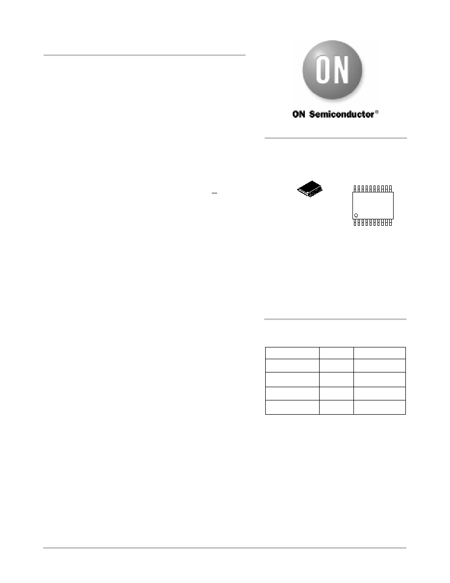
MARKING
DIAGRAM*
TSSOP≠20
DT SUFFIX
CASE 948E
Device
Package
Shipping
ORDERING INFORMATION
MC10EP29DT
TSSOP≠20
75 Units/Rail
MC10EP29DTR2
TSSOP≠20 2500 Tape & Reel
xxx = MC10 or 100
A
= Assembly Location
L
= Wafer Lot
Y
= Year
W
= Work Week
*For additional information, see Application Note
AND8002/D
xxx
EP29
ALYW
20
1
MC100EP29DT
TSSOP≠20
75 Units/Rail
MC100EP29DTR2 TSSOP≠20 2500 Tape & Reel
1
20
http://onsemi.com
MC10EP29, MC100EP29
http://onsemi.com
2
V
BB
Figure 1. 20≠Lead Pinout (Top View) and Logic Diagram
CLK0
D1
CLK1
17
18
16
15
14
13
12
4
3
5
6
7
8
9
Q0
11
10
Q0
S0
S1
V
CC
Q1
Q1
V
EE
D0
19
20
2
1
R0
V
CC
CLK0
D1
D0
CLK1
R1
CLK
D
S
R
Q
Q
CLK
D
R
S
Q
Q
R
L
L
H
L
H
TRUTH TABLE
S
L
L
L
H
H
D
L
H
X
X
X
CLK
Z
Z
X
X
X
Q
L
H
L
H
Undef
Z = LOW to HIGH Transition
X = Don't Care
Q
H
L
H
L
Undef
PIN DESCRIPTION
FUNCTION
ECL Differential Data Inputs
ECL Reset Inputs
ECL Differential Clock Inputs
ECL Differential Clock Inputs
ECL Set Inputs
ECL Differential Data Outputs
Reference Voltage Output
Positive Supply
Negative Supply
PIN
D0*, D0*; D1*, D1*
R0*, R1*
CLK0*, CLK0*
CLK1*, CLK1*
S0*, S1*
Q0, Q0; Q1, Q1
V
BB
V
CC
V
EE
Warning: All V
CC
and V
EE
pins must be externally connected
to Power Supply to guarantee proper operation.
* Pins will default LOW when left open.
ATTRIBUTES
Characteristics
Value
Internal Input Pulldown Resistor
75 k
W
Internal Input Pullup Resistor
N/A
ESD Protection
Human Body Model
Machine Model
Charged Device Model
> 2 kV
> 200 V
> 2 kV
Moisture Sensitivity, Indefinite Time Out of Drypack (Note 1)
Level 1
Flammability Rating
Oxygen Index: 28 to 34
UL 94 V≠0 @ 0.125 in
Transistor Count
383 Devices
Meets or exceeds JEDEC Spec EIA/JESD78 IC Latchup Test
1. For additional information, see Application Note AND8003/D.
MC10EP29, MC100EP29
http://onsemi.com
3
MAXIMUM RATINGS
(Note 2)
Symbol
Parameter
Condition 1
Condition 2
Rating
Units
V
CC
PECL Mode Power Supply
V
EE
= 0 V
6
V
V
EE
NECL Mode Power Supply
V
CC
= 0 V
≠6
V
V
I
PECL Mode Input Voltage
V
EE
= 0 V
V
I
V
CC
6
V
V
I
PECL Mode In ut Voltage
NECL Mode Input Voltage
V
EE
0 V
V
CC
= 0 V
V
I
V
CC
V
I
V
EE
6
≠6
V
V
I
out
Output Current
Continuous
Surge
50
100
mA
mA
I
BB
V
BB
Sink/Source
±
0.5
mA
TA
Operating Temperature Range
≠40 to +85
∞
C
T
stg
Storage Temperature Range
≠65 to +150
∞
C
q
JA
Thermal Resistance (Junction≠to≠Ambient)
0 LFPM
500 LFPM
20 TSSOP
20 TSSOP
140
100
∞
C/W
∞
C/W
q
JC
Thermal Resistance (Junction≠to≠Case)
std bd
20 TSSOP
23 to 41
∞
C/W
T
sol
Wave Solder
<2 to 3 sec @ 248
∞
C
265
∞
C
2. Maximum Ratings are those values beyond which device damage may occur.
10EP DC CHARACTERISTICS, PECL
V
CC
= 3.3 V, V
EE
= 0 V (Note 3)
≠40
∞
C
25
∞
C
85
∞
C
Symbol
Characteristic
Min
Typ
Max
Min
Typ
Max
Min
Typ
Max
Unit
I
EE
Power Supply Current
35
46
55
37
48
57
40
49
60
mA
V
OH
Output HIGH Voltage (Note 4)
2165
2290
2415
2230
2355
2480
2290
2415
2540
mV
V
OL
Output LOW Voltage (Note 4)
1365
1490
1615
1430
1555
1680
1490
1615
1740
mV
V
IH
Input HIGH Voltage (Single≠Ended)
2090
2415
2155
2480
2215
2540
mV
V
IL
Input LOW Voltage (Single≠Ended)
1365
1690
1460
1755
1490
1815
mV
V
BB
Output Voltage Reference
1790
1890
1990
1855
1955
2055
1915
2015
2115
mV
V
IHCMR
Input HIGH Voltage Common Mode
Range (Differential) (Note 5)
2.0
3.3
2.0
3.3
2.0
3.3
V
I
IH
Input HIGH Current
150
150
150
m
A
I
IL
Input LOW Current
0.5
0.5
0.5
m
A
NOTE: EP circuits are designed to meet the DC specifications shown in the above table after thermal equilibrium has been established. The
circuit is in a test socket or mounted on a printed circuit board and transverse airflow greater than 500 lfpm is maintained.
3. Input and output parameters vary 1:1 with V
CC
. V
EE
can vary +0.3 V to ≠2.2 V.
4. All loading with 50
W
to V
CC
≠2.0 volts.
5. V
IHCMR
min varies 1:1 with V
EE
, V
IHCMR
max varies 1:1 with V
CC
. The V
IHCMR
range is referenced to the most positive side of the differential
input signal.

MC10EP29, MC100EP29
http://onsemi.com
4
10EP DC CHARACTERISTICS, PECL
V
CC
= 5.0 V, V
EE
= 0 V (Note 6)
≠40
∞
C
25
∞
C
85
∞
C
Symbol
Characteristic
Min
Typ
Max
Min
Typ
Max
Min
Typ
Max
Unit
I
EE
Power Supply Current
35
46
55
37
48
57
40
49
60
mA
V
OH
Output HIGH Voltage (Note 7)
3865
3990
4115
3930
4055
4180
3990
4115
4240
mV
V
OL
Output LOW Voltage (Note 7)
3065
3190
3315
3130
3255
3380
3190
3315
3440
mV
V
IH
Input HIGH Voltage (Single≠Ended)
3790
4115
3855
4180
3915
4240
mV
V
IL
Input LOW Voltage (Single≠Ended)
3065
3390
3130
3455
3190
3515
mV
V
BB
Output Voltage Reference
3490
3590
3690
3555
3655
3755
3615
3715
3815
mV
V
IHCMR
Input HIGH Voltage Common Mode
Range (Differential) (Note 8)
2.0
5.0
2.0
5.0
2.0
5.0
V
I
IH
Input HIGH Current
150
150
150
m
A
I
IL
Input LOW Current
0.5
0.5
0.5
m
A
NOTE: EP circuits are designed to meet the DC specifications shown in the above table after thermal equilibrium has been established. The
circuit is in a test socket or mounted on a printed circuit board and transverse airflow greater than 500 lfpm is maintained.
6. Input and output parameters vary 1:1 with V
CC
. V
EE
can vary +2.0 V to ≠0.5 V.
7. All loading with 50
W
to V
CC
≠2.0 volts.
8. V
IHCMR
min varies 1:1 with V
EE
, V
IHCMR
max varies 1:1 with V
CC
. The V
IHCMR
range is referenced to the most positive side of the differential
input signal.
10EP DC CHARACTERISTICS, NECL
V
CC
= 0 V; V
EE
= ≠5.5 V to ≠3.0 V (Note 9)
≠40
∞
C
25
∞
C
85
∞
C
Symbol
Characteristic
Min
Typ
Max
Min
Typ
Max
Min
Typ
Max
Unit
I
EE
Power Supply Current
35
46
55
37
48
57
40
49
60
mA
V
OH
Output HIGH Voltage (Note 10)
≠1135
≠1010
≠885
≠1070
≠945
≠820
≠1010
≠885
≠760
mV
V
OL
Output LOW Voltage (Note 10)
≠1935
≠1810
≠1685
≠1870
≠1745
≠1620
≠1810
≠1685
≠1560
mV
V
IH
Input HIGH Voltage (Single≠Ended)
≠1210
≠885
≠1145
≠820
≠1085
≠760
mV
V
IL
Input LOW Voltage (Single≠Ended)
≠1935
≠1610
≠1870
≠1545
≠1810
≠1485
mV
V
BB
Output Voltage Reference
≠1510
≠1410
≠1310
≠1445
≠1345
≠1245
≠1385
≠1285
≠1185
mV
V
IHCMR
Input HIGH Voltage Common Mode
Range (Differential) (Note 11)
V
EE
+2.0
0.0
V
EE
+2.0
0.0
V
EE
+2.0
0.0
V
I
IH
Input HIGH Current
150
150
150
m
A
I
IL
Input LOW Current
0.5
0.5
0.5
m
A
NOTE: EP circuits are designed to meet the DC specifications shown in the above table after thermal equilibrium has been established. The
circuit is in a test socket or mounted on a printed circuit board and transverse airflow greater than 500 lfpm is maintained.
9. Input and output parameters vary 1:1 with V
CC
.
10. All loading with 50
W
to V
CC
≠2.0 volts.
11. V
IHCMR
min varies 1:1 with V
EE
, V
IHCMR
max varies 1:1 with V
CC
. The V
IHCMR
range is referenced to the most positive side of the differential
input signal.

MC10EP29, MC100EP29
http://onsemi.com
5
100EP DC CHARACTERISTICS, PECL
V
CC
= 3.3 V, V
EE
= 0 V (Note 12)
≠40
∞
C
25
∞
C
85
∞
C
Symbol
Characteristic
Min
Typ
Max
Min
Typ
Max
Min
Typ
Max
Unit
I
EE
Power Supply Current
35
46
55
37
48
57
40
49
60
mA
V
OH
Output HIGH Voltage (Note 13)
2155
2280
2405
2155
2280
2405
2155
2280
2405
mV
V
OL
Output LOW Voltage (Note 13)
1355
1480
1605
1355
1480
1605
1355
1480
1605
mV
V
IH
Input HIGH Voltage (Single≠Ended)
2075
2420
2075
2420
2075
2420
mV
V
IL
Input LOW Voltage (Single≠Ended)
1355
1675
1355
1675
1355
1675
mV
V
BB
Output Voltage Reference
1775
1875
1975
1775
1875
1975
1775
1875
1975
mV
V
IHCMR
Input HIGH Voltage Common Mode
Range (Differential) (Note 14)
2.0
3.3
2.0
3.3
2.0
3.3
V
I
IH
Input HIGH Current
150
150
150
m
A
I
IL
Input LOW Current
0.5
0.5
0.5
m
A
NOTE: EP circuits are designed to meet the DC specifications shown in the above table after thermal equilibrium has been established. The
circuit is in a test socket or mounted on a printed circuit board and transverse airflow greater than 500 lfpm is maintained.
12. Input and output parameters vary 1:1 with V
CC
. V
EE
can vary +0.3 V to ≠2.2 V.
13. All loading with 50
W
to V
CC
≠2.0 volts.
14. V
IHCMR
min varies 1:1 with V
EE
, V
IHCMR
max varies 1:1 with V
CC
. The V
IHCMR
range is referenced to the most positive side of the differential
input signal.
100EP DC CHARACTERISTICS, PECL
V
CC
= 5.0 V, V
EE
= 0 V (Note 15)
≠40
∞
C
25
∞
C
85
∞
C
Symbol
Characteristic
Min
Typ
Max
Min
Typ
Max
Min
Typ
Max
Unit
I
EE
Power Supply Current
35
46
55
37
48
57
40
49
60
mA
V
OH
Output HIGH Voltage (Note 16)
3855
3980
4105
3855
3980
4105
3855
3980
4105
mV
V
OL
Output LOW Voltage (Note 16)
3055
3180
3305
3055
3180
3305
3055
3180
3305
mV
V
IH
Input HIGH Voltage (Single≠Ended)
3775
4120
3775
4120
3775
4120
mV
V
IL
Input LOW Voltage (Single≠Ended)
3055
3375
3055
3375
3055
3375
mV
V
BB
Output Voltage Reference
3475
3575
3675
3475
3575
3675
3475
3575
3675
mV
V
IHCMR
Input HIGH Voltage Common Mode
Range (Differential) (Note 17)
2.0
5.0
2.0
5.0
2.0
5.0
V
I
IH
Input HIGH Current
150
150
150
m
A
I
IL
Input LOW Current
0.5
0.5
0.5
m
A
NOTE: EP circuits are designed to meet the DC specifications shown in the above table after thermal equilibrium has been established. The
circuit is in a test socket or mounted on a printed circuit board and transverse airflow greater than 500 lfpm is maintained.
15. Input and output parameters vary 1:1 with V
CC
. V
EE
can vary +2.0 V to ≠0.5 V.
16. All loading with 50
W
to V
CC
≠2.0 volts.
17. V
IHCMR
min varies 1:1 with V
EE
, V
IHCMR
max varies 1:1 with V
CC
. The V
IHCMR
range is referenced to the most positive side of the differential
input signal.