Äîêóìåíòàöèÿ è îïèñàíèÿ www.docs.chipfind.ru
©
Semiconductor Components Industries, LLC, 2004
June, 2004 - Rev. 6
1
Publication Order Number:
MC10EP451/D
MC10EP451, MC100EP451
3.3V / 5V ECL 6-Bit
Differential Register with
Master Reset
The MC10/100EP451 is a 6-bit fully differential register with
common clock and single-ended Master Reset (MR). It is ideal for
very high frequency applications where a registered data path is
necessary.
All inputs have a 75 k
W pulldown resistor internally. Differential
inputs have an override clamp. Unused differential register inputs can
be left open and will default LOW. When the differential inputs are
forced to < V
EE
+ 1.2 V, the clamp will override and force the output to
a default state. When in the default state, and since the flip-flop is edge
triggered, the output reaches a determined, but not predicted, valid
state.
The positive transition of CLK (pin 4) will latch the registers.
Master Reset (MR) HIGH will asynchronously reset all registers
forcing Q outputs to go LOW.
The 100 Series contains temperature compensation.
·
450 ps Typical Propagation Delay
·
Maximum Frequency > 3.0 GHz Typical
·
Asynchronous Master Reset
·
20 ps Skew Within Device, 35 ps Skew Device-To-Device
·
PECL Mode Operating Range: V
CC
= 3.0 V to 5.5 V
With V
EE
= 0 V
·
NECL Mode Operating Range: V
CC
= 0 V
With V
EE
= -3.0 V to -5.5 V
·
Open Input Default State
·
Safety Clamp on Inputs
·
Pb-Free Packages are Available*
*For additional information on our Pb-Free strategy and soldering details, please
download the ON Semiconductor Soldering and Mounting Techniques
Reference Manual, SOLDERRM/D.
LQFP-32
FA SUFFIX
CASE 873A
MARKING
DIAGRAM*
MCxxx
AWLYYWW
xxx = 10 or 100
A
= Assembly Location
WL = Wafer Lot
YY = Year
WW = Work Week
EP451
1
32
http://onsemi.com
See detailed ordering and shipping information in the package
dimensions section on page 7 of this data sheet.
ORDERING INFORMATION
*For additional marking information, refer to
Application Note AND8002/D.
MC10EP451, MC100EP451
http://onsemi.com
2
Q1
25
26
27
28
29
30
31
32
15
14
13
12
11
10
9
1
2
3
4
5
6
7
8
24
23
22
21
20
19
18
17
16
Q1
Q2
Q2
V
CC
Q3
Q3
V
CC
D1
D2
D2
MR
V
EE
D3
D3
D4
Q0
Q0
V
CC
CLK
CLK
D0
D1
Q4
Q4
V
EE
Q5
Q5
D5
D4
D5
D0
PIN
D [0:5]*, D [0:5]*
ECL Differential Data Inputs
FUNCTION
MR*
CLK*, CLK*
ECL Differential Clock Inputs
ECL Master Reset Input
ECL Differential Data Outputs
V
CC
Positive Supply
V
EE
Negative Supply
Figure 1. LQFP-32 Pinout (Top View)
Warning: All V
CC
and V
EE
pins must be externally connected to Power
Supply to guarantee proper operation.
Figure 2. Logic Diagram
Q [0:5], Q [0:5]
D
Q
R
D
Q
R
D
Q
R
D
Q
R
D
Q
R
D
Q
R
MR
CLK
CLK
D5
D5
D4
D4
D3
D3
D2
D2
D1
D1
D0
D0
Q0
Q0
Q1
Q1
Q2
Q2
Q3
Q3
Q4
Q4
Q5
Q5
MC10EP451
MC100EP451
* Pins will default LOW when left open.
V
EE
Table 1. PIN DESCRIPTION
Table 2. ATTRIBUTES
Characteristics
Value
Internal Input Pulldown Resistor
75 k
W
Internal Input Pullup Resistor
N/A
ESD Protection
Human Body Model
Machine Model
Charged Device Model
> 2 kV
> 200 V
> 2 kV
Moisture Sensitivity (Note 1)
Level 2
Flammability Rating
Oxygen Index: 28 to 34
UL 94 V-0 @ 0.125 in
Transistor Count
919 Devices
Meets or exceeds JEDEC Spec EIA/JESD78 IC Latchup Test
1. For additional information, see Application Note AND8003/D.
MC10EP451, MC100EP451
http://onsemi.com
3
Table 3. MAXIMUM RATINGS
Symbol
Parameter
Condition 1
Condition 2
Rating
Unit
V
CC
PECL Mode Power Supply
V
EE
= 0 V
6
V
V
EE
NECL Mode Power Supply
V
CC
= 0 V
-6
V
V
I
PECL Mode Input Voltage
NECL Mode Input Voltage
V
EE
= 0 V
V
CC
= 0 V
V
I
v
V
CC
V
I
w
V
EE
6
-6
V
V
I
out
Output Current
Continuous
Surge
50
100
mA
mA
T
A
Operating Temperature Range
-40 to +85
°
C
T
stg
Storage Temperature Range
-65 to +150
°
C
q
JA
Thermal Resistance (Junction to Ambient)
0 lfpm
500 lfpm
LQFP-32
LQFP-32
80
55
°
C/W
°
C/W
q
JC
Thermal Resistance (Junction to Case)
Standard Board
LQFP-32
12 to 17
°
C/W
T
sol
Wave Solder
<2 to 3 sec @ 248
°
C
265
°
C
Maximum ratings are those values beyond which device damage can occur. Maximum ratings applied to the device are individual stress limit
values (not normal operating conditions) and are not valid simultaneously. If these limits are exceeded, device functional operation is not implied,
damage may occur and reliability may be affected.
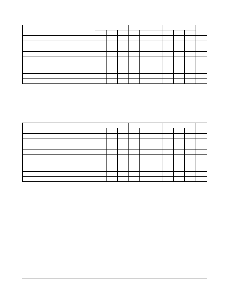
Table 4. 10EP DC CHARACTERISTICS, PECL
V
CC
= 3.3 V, V
EE
= 0 V (Note 2)
-40
°
C
25
°
C
85
°
C
Symbol
Characteristic
Min
Typ
Max
Min
Typ
Max
Min
Typ
Max
Unit
I
EE
Power Supply Current
80
95
125
80
95
125
80
95
125
mA
V
OH
Output HIGH Voltage (Note 3)
2165
2290
2415
2230
2355
2480
2290
2415
2540
mV
V
OL
Output LOW Voltage (Note 3)
1365
1490
1615
1430
1555
1680
1470
1615
1740
mV
V
IH
Input HIGH Voltage (Single-Ended)
2090
2415
2155
2480
2215
2540
mV
V
IL
Input LOW Voltage (Single-Ended)
1365
1690
1430
1755
1490
1815
mV
V
IHCMR
Input HIGH Voltage Common Mode
Range (Differential Configuration)
(Note 4)
2.0
3.3
2.0
3.3
2.0
3.3
V
I
IH
Input HIGH Current
150
150
150
m
A
I
IL
Input LOW Current
0.5
0.5
0.5
m
A
NOTE: Device will meet the specifications after thermal equilibrium has been established when mounted in a test socket or printed circuit
board with maintained transverse airflow greater than 500 lfpm. Electrical parameters are guaranteed only over the declared
operating temperature range. Functional operation of the device exceeding these conditions is not implied. Device specification limit
values are applied individually under normal operating conditions and not valid simultaneously.
2. Input and output parameters vary 1:1 with V
CC
. V
EE
can vary +0.3 V to -2.2 V.
3. All loading with 50
W
to V
CC
- 2.0 V.
4. V
IHCMR
min varies 1:1 with V
EE
, V
IHCMR
max varies 1:1 with V
CC
. The V
IHCMR
range is referenced to the most positive side of the differential
input signal.
MC10EP451, MC100EP451
http://onsemi.com
4
Table 5. 10EP DC CHARACTERISTICS, PECL
V
CC
= 5.0 V, V
EE
= 0 V (Note 5)
-40
°
C
25
°
C
85
°
C
Symbol
Characteristic
Min
Typ
Max
Min
Typ
Max
Min
Typ
Max
Unit
I
EE
Power Supply Current
80
95
125
80
95
125
80
95
125
mA
V
OH
Output HIGH Voltage (Note 6)
3865
3990
4115
3930
4055
4180
3990
4115
4240
mV
V
OL
Output LOW Voltage (Note 6)
3065
3190
3315
3130
3255
3380
3170
3315
3440
mV
V
IH
Input HIGH Voltage (Single-Ended)
3790
4115
3855
4180
3915
4240
mV
V
IL
Input LOW Voltage (Single-Ended)
3065
3390
3130
3455
3190
3515
mV
V
IHCMR
Input HIGH Voltage Common Mode
Range (Differential Configuration)
(Note 7)
2.0
5.0
2.0
5.0
2.0
5.0
V
I
IH
Input HIGH Current
150
150
150
m
A
I
IL
Input LOW Current
0.5
0.5
0.5
m
A
NOTE: Device will meet the specifications after thermal equilibrium has been established when mounted in a test socket or printed circuit
board with maintained transverse airflow greater than 500 lfpm. Electrical parameters are guaranteed only over the declared
operating temperature range. Functional operation of the device exceeding these conditions is not implied. Device specification limit
values are applied individually under normal operating conditions and not valid simultaneously.
5. Input and output parameters vary 1:1 with V
CC
. V
EE
can vary +2.0 V to -0.5 V.
6. All loading with 50
W
to V
CC
- 2.0 V.
7. V
IHCMR
min varies 1:1 with V
EE
, V
IHCMR
max varies 1:1 with V
CC
. The V
IHCMR
range is referenced to the most positive side of the differential
input signal.
Table 6. 10EP DC CHARACTERISTICS, NECL
V
CC
= 0 V, V
EE
= -5.5 V to -3.0 V (Note 8)
-40
°
C
25
°
C
85
°
C
Symbol
Characteristic
Min
Typ
Max
Min
Typ
Max
Min
Typ
Max
Unit
I
EE
Power Supply Current
80
95
125
80
95
125
80
95
125
mA
V
OH
Output HIGH Voltage (Note 9)
-1135
-1010
-885
-1070
-945
-820
-1010
-885
-760
mV
V
OL
Output LOW Voltage (Note 9)
-1935
-1810
-1685
-1870
-1745
-1620
-1830
-1685
-1560
mV
V
IH
Input HIGH Voltage (Single-Ended)
-1210
-885
-1145
-820
-1085
-760
mV
V
IL
Input LOW Voltage (Single-Ended)
-1935
-1610
-1870
-1545
-1810
-1485
mV
V
IHCMR
Input HIGH Voltage Common Mode
Range (Differential Configuration)
(Note 10)
V
EE
+2.0
0.0
V
EE
+2.0
0.0
V
EE
+2.0
0.0
V
I
IH
Input HIGH Current
150
150
150
m
A
I
IL
Input LOW Current
0.5
0.5
0.5
m
A
NOTE: Device will meet the specifications after thermal equilibrium has been established when mounted in a test socket or printed circuit
board with maintained transverse airflow greater than 500 lfpm. Electrical parameters are guaranteed only over the declared
operating temperature range. Functional operation of the device exceeding these conditions is not implied. Device specification limit
values are applied individually under normal operating conditions and not valid simultaneously.
8. Input and output parameters vary 1:1 with V
CC
.
9. All loading with 50
W
to V
CC
- 2.0 V.
10. V
IHCMR
min varies 1:1 with V
EE
, V
IHCMR
max varies 1:1 with V
CC
. The V
IHCMR
range is referenced to the most positive side of the differential
input signal.
MC10EP451, MC100EP451
http://onsemi.com
5
Table 7. 100EP DC CHARACTERISTICS, PECL
V
CC
= 3.3 V, V
EE
= 0 V (Note 11)
-40
°
C
25
°
C
85
°
C
Symbol
Characteristic
Min
Typ
Max
Min
Typ
Max
Min
Typ
Max
Unit
I
EE
Power Supply Current
85
105
135
85
105
135
85
105
135
mA
V
OH
Output HIGH Voltage (Note 12)
2155
2280
2405
2155
2280
2405
2155
2280
2405
mV
V
OL
Output LOW Voltage (Note 12)
1355
1480
1605
1355
1480
1605
1355
1480
1605
mV
V
IH
Input HIGH Voltage (Single-Ended)
2075
2420
2075
2420
2075
2420
mV
V
IL
Input LOW Voltage (Single-Ended)
1355
1675
1355
1675
1355
1675
mV
V
IHCMR
Input HIGH Voltage Common Mode
Range (Differential Configuration)
(Note 13)
2.0
3.3
2.0
3.3
2.0
3.3
V
I
IH
Input HIGH Current
150
150
150
m
A
I
IL
Input LOW Current
0.5
0.5
0.5
m
A
NOTE: Device will meet the specifications after thermal equilibrium has been established when mounted in a test socket or printed circuit
board with maintained transverse airflow greater than 500 lfpm. Electrical parameters are guaranteed only over the declared
operating temperature range. Functional operation of the device exceeding these conditions is not implied. Device specification limit
values are applied individually under normal operating conditions and not valid simultaneously.
11. Input and output parameters vary 1:1 with V
CC
. V
EE
can vary +0.3 V to -2.2 V.
12. All loading with 50
W
to V
CC
- 2.0 V.
13. V
IHCMR
min varies 1:1 with V
EE
, V
IHCMR
max varies 1:1 with V
CC
. The V
IHCMR
range is referenced to the most positive side of the differential
input signal.
Table 8. 100EP DC CHARACTERISTICS, PECL
V
CC
= 5.0 V, V
EE
= 0 V (Note 14)
-40
°
C
25
°
C
85
°
C
Symbol
Characteristic
Min
Typ
Max
Min
Typ
Max
Min
Typ
Max
Unit
I
EE
Power Supply Current
85
105
135
85
105
135
85
105
135
mA
V
OH
Output HIGH Voltage (Note 15)
3855
3980
4105
3855
3980
4105
3855
3980
4105
mV
V
OL
Output LOW Voltage (Note 15)
3055
3180
3305
3055
3180
3305
3055
3180
3305
mV
V
IH
Input HIGH Voltage (Single-Ended)
3775
4120
3775
4120
3775
4120
mV
V
IL
Input LOW Voltage (Single-Ended)
3055
3375
3055
3375
3055
3375
mV
V
IHCMR
Input HIGH Voltage Common Mode
Range (Differential Configuration)
(Note 16)
2.0
5.0
2.0
5.0
2.0
5.0
V
I
IH
Input HIGH Current
150
150
150
m
A
I
IL
Input LOW Current
0.5
0.5
0.5
m
A
NOTE: Device will meet the specifications after thermal equilibrium has been established when mounted in a test socket or printed circuit
board with maintained transverse airflow greater than 500 lfpm. Electrical parameters are guaranteed only over the declared
operating temperature range. Functional operation of the device exceeding these conditions is not implied. Device specification limit
values are applied individually under normal operating conditions and not valid simultaneously.
14. Input and output parameters vary 1:1 with V
CC
. V
EE
can vary +2.0 V to -0.5 V.
15. All loading with 50
W
to V
CC
- 2.0 V.
16. V
IHCMR
min varies 1:1 with V
EE
, V
IHCMR
max varies 1:1 with V
CC
. The V
IHCMR
range is referenced to the most positive side of the differential
input signal.