©
Semiconductor Components Industries, LLC, 2000
October, 2000 ≠ Rev. 1
1
Publication Order Number:
MC100LVEL31/D
MC100LVEL31
3.3V ECL D Flip Flop
with Set and Reset
The MC100LVEL31 is a D flip-flop with set and reset. The device is
functionally equivalent to the EL31 device but operates from a 3.3 V
supply. With propagation delays and output transition times essentially
equivalent to the EL31, the LVEL31 is ideally suited for those
applications which require the ultimate in AC performance at low power
supply voltages.
Both set and reset inputs are asynchronous, level triggered signals.
Data enters the master portion of the flip-flop when clock is LOW and is
transferred to the slave, and thus the outputs, upon a positive transition of
the clock.
∑
475 ps Typical Propagation Delay
∑
2.9 GHz Toggle Frequency
∑
ESD Protection: >4 KV HBM, >200 V MM
∑
The 100 Series Contains Temperature Compensation
∑
PECL Mode Operating Range: V
CC
= 3.0 V to 3.8 V
with V
EE
= 0 V
∑
NECL Mode Operating Range: V
CC
= 0 V
with V
EE
= ≠3.0 V to ≠3.8 V
∑
Internal Input Pulldown Resistors
∑
Meets or Exceeds JEDEC Spec EIA/JESD78 IC Latchup Test
∑
Moisture Sensitivity Level 1
For Additional Information, see Application Note AND8003/D
∑
Flammability Rating: UL≠94 code V≠0 @ 1/8",
Oxygen Index 28 to 34
∑
Transistor Count = 121 devices
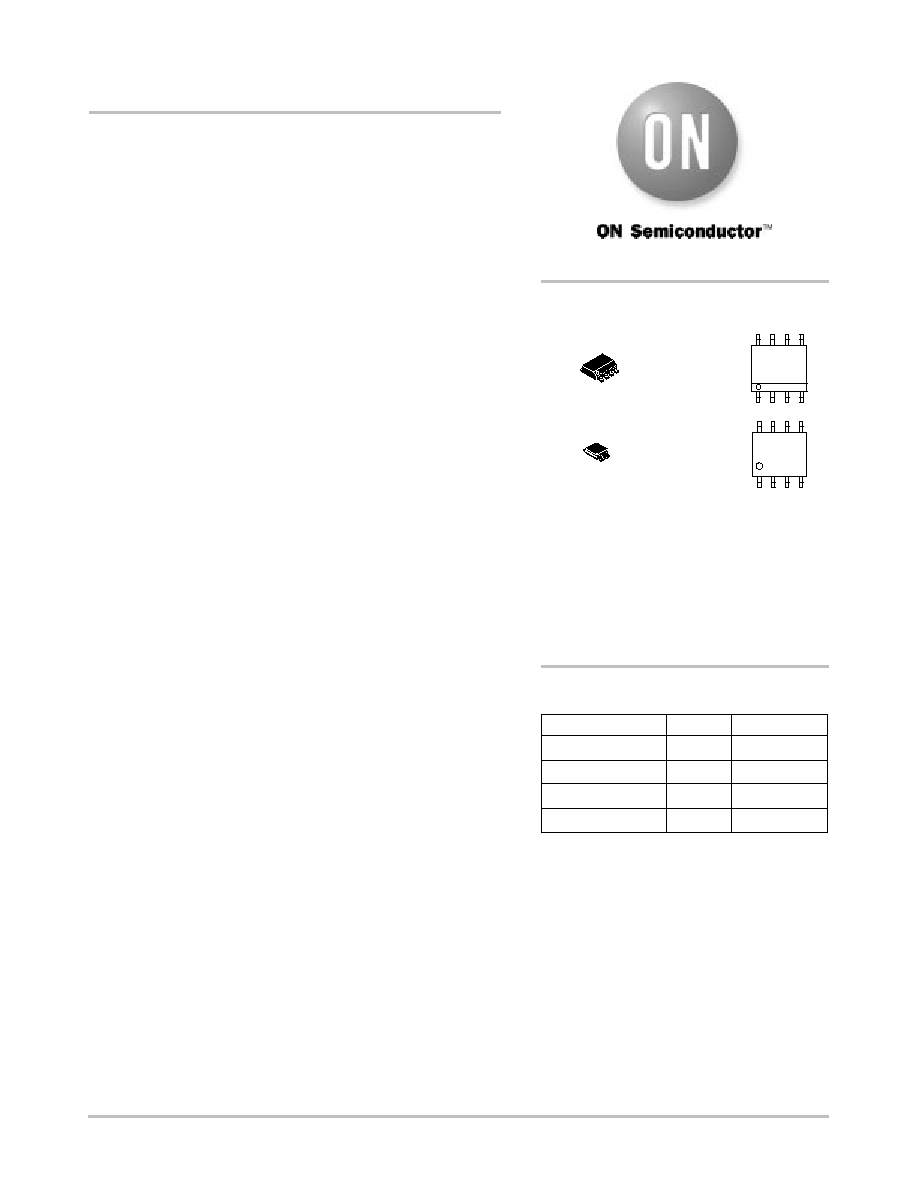
http://onsemi.com
Device
Package
Shipping
ORDERING INFORMATION
MC100LVEL31D
SO≠8
98 Units / Rail
MC100LVEL31DR2
SO≠8
2500 / Reel
MC100LVEL31DT
TSSOP≠8
98 Units / Rail
MC100LVEL31DTR2
TSSOP≠8
2500 / Reel
*For additional information, see Application Note
AND8002/D
SO≠8
D SUFFIX
CASE 751
MARKING
DIAGRAMS*
TSSOP≠8
DT SUFFIX
CASE 948R
A = Assembly Location
L = Wafer Lot
Y = Year
W = Work Week
1
8
1
8
ALYW
KVL31
1
8
ALYW
KV31
1
8
MC100LVEL31
http://onsemi.com
2
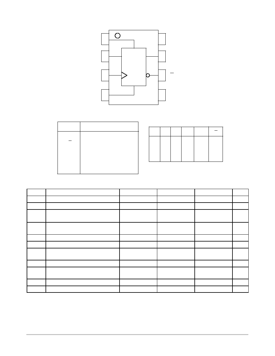
LOGIC DIAGRAM AND PINOUT ASSIGNMENT
1
2
3
4
5
6
7
8
Q
V
EE
V
CC
D
Q
CLK
R
D
S
Flip Flop
R
S
PIN
FUNCTION
CLK
ECL Clock Input
Q, Q
ECL Differential Data Outputs
D
ECL Data Input
R
ECL Reset Input
S
ECL Set Input
V
CC
Positive Supply
V
EE
Negative Supply
PIN DESCRIPTION
D
L
H
X
X
X
TRUTH TABLE
S
L
L
H
L
H
R
L
L
L
H
H
CLK
Z
Z
X
X
X
Q
L
H
H
L
Undef
Z = LOW to HIGH Transition
X = Don't Care
Q
H
L
L
H
Undef
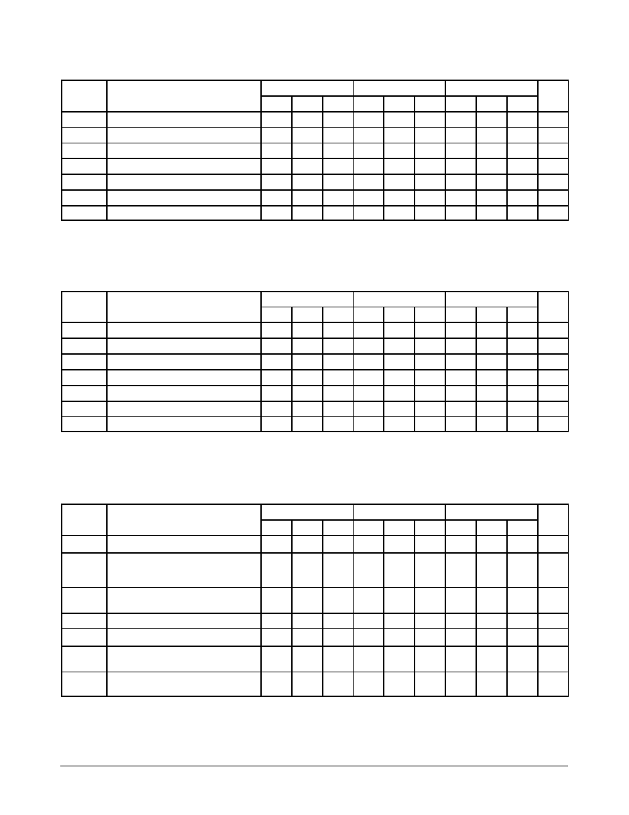
MAXIMUM RATINGS
(Note 1.)
Symbol
Parameter
Condition 1
Condition 2
Rating
Units
V
CC
PECL Mode Power Supply
V
EE
= 0 V
8 to 0
V
V
EE
NECL Mode Power Supply
V
CC
= 0 V
≠8 to 0
V
V
I
PECL Mode Input Voltage
V
EE
= 0 V
V
I
V
CC
6 to 0
V
I
C
ode
u
o age
NECL Mode Input Voltage
EE
0
V
CC
= 0 V
I
CC
V
I
V
EE
6 o 0
≠6 to 0
V
I
out
Output Current
Continuous
Surge
50
100
mA
mA
TA
Operating Temperature Range
≠40 to +85
∞
C
T
stg
Storage Temperature Range
≠65 to +150
∞
C
JA
Thermal Resistance (Junction to Ambient)
0 LFPM
500 LFPM
8 SOIC
8 SOIC
190
130
∞
C/W
∞
C/W
JC
Thermal Resistance (Junction to Case)
std bd
8 SOIC
41 to 44
±
5%
∞
C/W
JA
Thermal Resistance (Junction to Ambient)
0 LFPM
500 LFPM
8 TSSOP
8 TSSOP
185
140
∞
C/W
∞
C/W
JC
Thermal Resistance (Junction to Case)
std bd
8 TSSOP
41 to 44
±
5%
∞
C/W
T
sol
Wave Solder
<2 to 3 sec @ 248
∞
C
265
∞
C
1. Maximum Ratings are those values beyond which device damage may occur.
MC100LVEL31
http://onsemi.com
3
LVPECL DC CHARACTERISTICS
V
CC
= 3.3 V; V
EE
= 0.0 V (Note 1)
≠40
∞
C
25
∞
C
85
∞
C
Symbol
Characteristic
Min
Typ
Max
Min
Typ
Max
Min
Typ
Max
Unit
I
EE
Power Supply Current
30
35
30
35
32
38
mA
V
OH
Output HIGH Voltage (Note 2.)
2215
2295
2420
2275
2345
2420
2275
2345
2420
mV
V
OL
Output LOW Voltage (Note 2.)
1470
1605
1745
1490
1595
1680
1490
1595
1680
mV
V
IH
Input HIGH Voltage
2135
2420
2135
2420
2135
2420
mV
V
IL
Input LOW Voltage
1490
1825
1490
1825
1490
1825
mV
I
IH
Input HIGH Current
150
150
150
µ
A
I
IL
Input LOW Current
0.5
0.5
0.5
µ
A
NOTE: Devices are designed to meet the DC specifications shown in the above table, after thermal equilibrium has been established. The
circuit is in a test socket or mounted on a printed circuit board and transverse air flow greater than 500 lfpm is maintained.
1. Input and output parameters vary 1:1 with V
CC
. V
EE
can vary
±
0.3 V.
2. Outputs are terminated through a 50 ohm resistor to V
CC
≠2 volts.
LVNECL DC CHARACTERISTICS
V
CC
= 0.0 V; V
EE
= ≠3.3 V (Note 1)
≠40
∞
C
25
∞
C
85
∞
C
Symbol
Characteristic
Min
Typ
Max
Min
Typ
Max
Min
Typ
Max
Unit
I
EE
Power Supply Current
30
35
30
35
32
38
mA
V
OH
Output HIGH Voltage (Note 2.)
≠1085
≠1005
≠880
≠1025
≠955
≠880
≠1025
≠955
≠880
mV
V
OL
Output LOW Voltage (Note 2.)
≠1830
≠1695
≠1555
≠1810
≠1705
≠1620
≠1810
≠1705
≠1620
mV
V
IH
Input HIGH Voltage
≠1165
≠880
≠1165
≠880
≠1165
≠880
mV
V
IL
Input LOW Voltage
≠1810
≠1475
≠1810
≠1475
≠1810
≠1475
mV
I
IH
Input HIGH Current
150
150
150
µ
A
I
IL
Input LOW Current
0.5
0.5
0.5
µ
A
NOTE: Devices are designed to meet the DC specifications shown in the above table, after thermal equilibrium has been established. The
circuit is in a test socket or mounted on a printed circuit board and transverse air flow greater than 500 lfpm is maintained.
1. Input and output parameters vary 1:1 with V
CC
. V
EE
can vary
±
0.3 V.
2. Outputs are terminated through a 50 ohm resistor to V
CC
≠2 volts.
AC CHARACTERISTICS
V
CC
= 3.3 V; V
EE
= 0.0 V or V
CC
= 0.0 V; V
EE
= ≠3.3 V (Note 1.)
≠40
∞
C
25
∞
C
85
∞
C
Symbol
Characteristic
Min
Typ
Max
Min
Typ
Max
Min
Typ
Max
Unit
f
max
Maximum Toggle Frequency
2.7
2.9
2.9
GHz
t
PLH
t
PHL
Propagation Delay
to Output
CLK
S, R
365
385
465
475
580
620
375
395
475
485
590
630
415
435
530
525
630
670
ps
t
S
t
H
Setup Time
Hold Time
150
250
0
100
150
250
0
100
150
250
0
100
ps
t
RR
Set/Reset Recovery
400
200
400
200
400
200
ps
t
JITTER
Cycle≠to≠Cycle Jitter
TBD
TBD
TBD
ps
t
PW
Minimum Pulse Width
CLK
Set, Reset
340
600
340
600
340
600
ps
t
r
t
f
Output Rise/Fall Times Q
(20% ≠ 80%)
120
220
320
120
220
320
120
220
320
ps
1. V
EE
can vary
±
0.3 V.
MC100LVEL31
http://onsemi.com
4
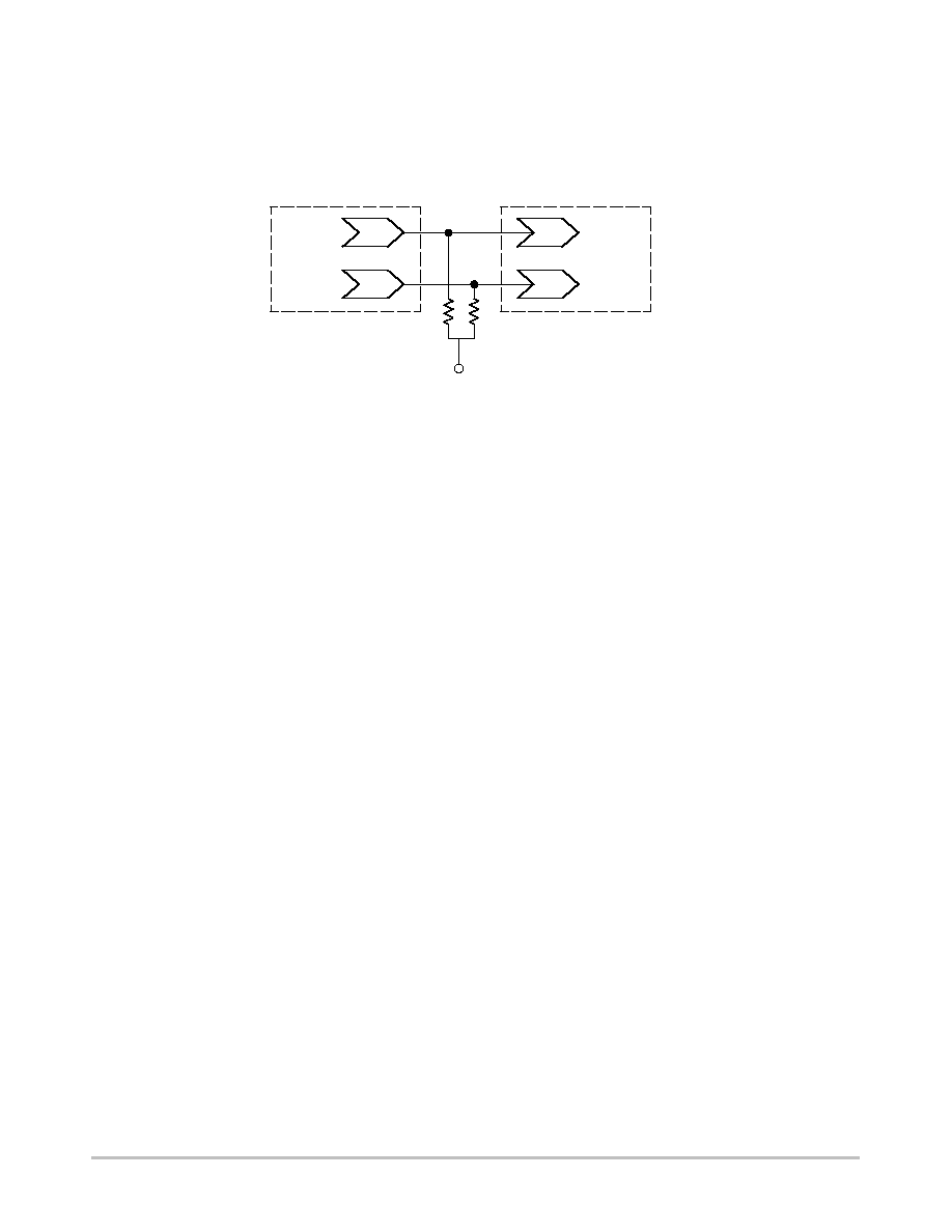
V TT = V CC ≠ 2.0 V
Figure 1. Typical Termination for Output Driver and Device Evaluation
(See Application Note AND8020 ≠ Termination of ECL Logic Devices.)
W
Driver
Device
Receiver
Device
Q
Qb
D
Db
50
W
50
V TT
Resource Reference of Application Notes
AN1404
≠
ECLinPS Circuit Performance at Non≠Standard V
IH
Levels
AN1405
≠
ECL Clock Distribution Techniques
AN1406
≠
Designing with PECL (ECL at +5.0 V)
AN1503
≠
ECLinPS I/O SPICE Modeling Kit
AN1504
≠
Metastability and the ECLinPS Family
AN1560
≠
Low Voltage ECLinPS SPICE Modeling Kit
AN1568
≠
Interfacing Between LVDS and ECL
AN1596
≠
ECLinPS Lite Translator ELT Family SPICE I/O Model Kit
AN1650
≠
Using Wire≠OR Ties in ECLinPS Designs
AN1672
≠
The ECL Translator Guide
AND8001
≠
Odd Number Counters Design
AND8002
≠
Marking and Date Codes
AND8020
≠
Termination of ECL Logic Devices
MC100LVEL31
http://onsemi.com
5
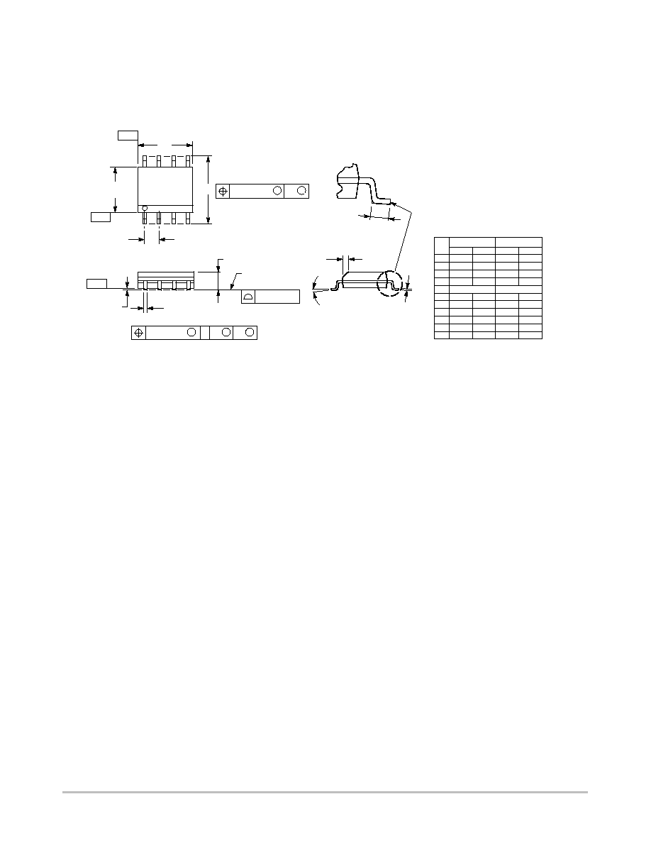
PACKAGE DIMENSIONS
SO≠8
D SUFFIX
PLASTIC SOIC PACKAGE
CASE 751≠07
ISSUE V
SEATING
PLANE
1
4
5
8
N
J
X 45
_
K
NOTES:
1. DIMENSIONING AND TOLERANCING PER ANSI
Y14.5M, 1982.
2. CONTROLLING DIMENSION: MILLIMETER.
3. DIMENSION A AND B DO NOT INCLUDE MOLD
PROTRUSION.
4. MAXIMUM MOLD PROTRUSION 0.15 (0.006) PER
SIDE.
5. DIMENSION D DOES NOT INCLUDE DAMBAR
PROTRUSION. ALLOWABLE DAMBAR
PROTRUSION SHALL BE 0.127 (0.005) TOTAL IN
EXCESS OF THE D DIMENSION AT MAXIMUM
MATERIAL CONDITION.
A
B
S
D
H
C
0.10 (0.004)
DIM
A
MIN
MAX
MIN
MAX
INCHES
4.80
5.00
0.189
0.197
MILLIMETERS
B
3.80
4.00
0.150
0.157
C
1.35
1.75
0.053
0.069
D
0.33
0.51
0.013
0.020
G
1.27 BSC
0.050 BSC
H
0.10
0.25
0.004
0.010
J
0.19
0.25
0.007
0.010
K
0.40
1.27
0.016
0.050
M
0
8
0
8
N
0.25
0.50
0.010
0.020
S
5.80
6.20
0.228
0.244
≠X≠
≠Y≠
G
M
Y
M
0.25 (0.010)
≠Z≠
Y
M
0.25 (0.010)
Z
S
X
S
M
_
_
_
_