
©
Semiconductor Components Industries, LLC, 2000
October, 2000 ≠ Rev. 2
1
Publication Order Number:
MC100LVEL51/D
MC100LVEL51
3.3V ECL Differential Clock
D Flip Flop
The MC100LVEL51 is a differential clock D flip-flop with reset. The
device is functionally equivalent to the EL51 device, but operates from a
3.3 V supply. With propagation delays and output transition times
essentially equal to the EL51, the LVEL51 is ideally suited for those
applications which require the ultimate in AC performance at 3.3 V V
CC
.
The reset input is an asynchronous, level triggered signal. Data enters
the master portion of the flip-flop when the clock is LOW and is
transferred to the slave, and thus the outputs, upon a positive transition of
the clock. The differential clock inputs of the LVEL51 allow the device to
be used as a negative edge triggered flip-flop.
The differential input employs clamp circuitry to maintain stability
under open input conditions. When left open, the CLK input will be
pulled down to V
EE
and the CLK input will be biased at V
CC
/2.
∑
475 ps Propagation Delay
∑
2.8 GHz Toggle Frequency
∑
ESD Protection: >4 KV HBM, >200 V MM
∑
The 100 Series Contains Temperature Compensation
∑
PECL Mode Operating Range: V
CC
= 3.0 V to 3.8 V
with V
EE
= 0 V
∑
NECL Mode Operating Range: V
CC
= 0 V
with V
EE
= ≠3.0 V to ≠3.8 V
∑
Internal Input Pulldown Resistors
∑
Meets or Exceeds JEDEC Spec EIA/JESD78 IC Latchup Test
∑
Moisture Sensitivity Level 1
For Additional Information, see Application Note AND8003/D
∑
Flammability Rating: UL≠94 code V≠0 @ 1/8",
Oxygen Index 28 to 34
∑
Transistor Count = 114 devices
http://onsemi.com
Device
Package
Shipping
ORDERING INFORMATION
MC100LVEL51D
SO≠8
98 Units / Rail
MC100LVEL51DR2
SO≠8
2500 / Reel
MC100LVEL51DT
TSSOP≠8
98 Units / Rail
MC100LVEL51DTR2 TSSOP≠8
2500 / Reel
*For additional information, see Application Note
AND8002/D
SO≠8
D SUFFIX
CASE 751
MARKING
DIAGRAMS*
TSSOP≠8
DT SUFFIX
CASE 948R
A = Assembly Location
L = Wafer Lot
Y = Year
W = Work Week
1
8
1
8
ALYW
KVL51
1
8
ALYW
KV51
1
8
MC100LVEL51
http://onsemi.com
2
1
2
3
4
5
6
7
8
Q
V
EE
V
CC
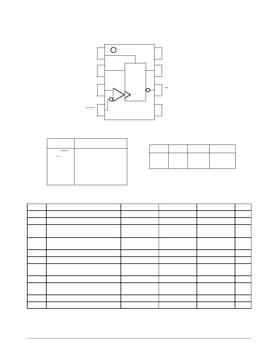
LOGIC DIAGRAM AND PINOUT ASSIGNMENT
D
Q
CLK
CLK
R
D
R
Flip-Flop
TRUTH TABLE
D
L
H
X
R
L
L
H
CLK
Z
Z
X
Q
L
H
L
Z = LOW to HIGH Transition
X = Don't Care
CLK, CLK
ECL Differential Clock Input
Q, Q
ECL Differential Output
D
ECL D Input
R
ECL Reset Input
V
CC
Positive Supp;y
V
EE
Negative Supply
PIN DESCRIPTION
PIN
FUNCTION
MAXIMUM RATINGS
(Note 1.)
Symbol
Parameter
Condition 1
Condition 2
Rating
Units
V
CC
PECL Mode Power Supply
V
EE
= 0 V
8 to 0
V
V
EE
NECL Mode Power Supply
V
CC
= 0 V
≠8 to 0
V
V
I
PECL Mode Input Voltage
V
EE
= 0 V
V
I
V
CC
6 to 0
V
I
C
ode
u
o age
NECL Mode Input Voltage
EE
0
V
CC
= 0 V
I
CC
V
I
V
EE
6 o 0
≠6 to 0
V
I
out
Output Current
Continuous
Surge
50
100
mA
mA
TA
Operating Temperature Range
≠40 to +85
∞
C
T
stg
Storage Temperature Range
≠65 to +150
∞
C
JA
Thermal Resistance (Junction to Ambient)
0 LFPM
500 LFPM
8 SOIC
8 SOIC
190
130
∞
C/W
∞
C/W
JC
Thermal Resistance (Junction to Case)
std bd
8 SOIC
41 to 44
±
5%
∞
C/W
JA
Thermal Resistance (Junction to Ambient)
0 LFPM
500 LFPM
8 TSSOP
8 TSSOP
185
140
∞
C/W
∞
C/W
JC
Thermal Resistance (Junction to Case)
std bd
8 TSSOP
41 to 44
±
5%
∞
C/W
T
sol
Wave Solder
<2 to 3 sec @ 248
∞
C
265
∞
C
1. Maximum Ratings are those values beyond which device damage may occur.
MC100LVEL51
http://onsemi.com
3
LVPECL DC CHARACTERISTICS
V
CC
= 3.3 V; V
EE
= 0.0 V (Note 1)
≠40
∞
C
25
∞
C
85
∞
C
Symbol
Characteristic
Min
Typ
Max
Min
Typ
Max
Min
Typ
Max
Unit
I
EE
Power Supply Current
30
35
30
35
32
37
mA
V
OH
Output HIGH Voltage (Note 2.)
2215
2295
2420
2275
2345
2420
2275
2345
2420
mV
V
OL
Output LOW Voltage (Note 2.)
1470
1605
1745
1490
1595
1680
1490
1595
1680
mV
V
IH
Input HIGH Voltage (Single Ended)
2135
2420
2135
2420
2135
2420
mV
V
IL
Input LOW Voltage (Single Ended)
1490
1825
1490
1825
1490
1825
mV
V
IHCMR
Input HIGH Voltage Common Mode
Range (Differential) (Note 3.)
Vpp < 500 mV
Vpp
y
500 mV
1.2
1.4
3.0
3.0
1.1
1.3
3.0
3.0
1.1
1.3
3.0
3.0
V
V
I
IH
Input HIGH Current
150
150
150
µ
A
I
IL
Input LOW Current
Others
CLK
0.5
≠600
0.5
≠600
0.5
≠600
µ
A
µ
A
NOTE: Devices are designed to meet the DC specifications shown in the above table, after thermal equilibrium has been established. The
circuit is in a test socket or mounted on a printed circuit board and transverse air flow greater than 500 lfpm is maintained.
1. Input and output parameters vary 1:1 with V
CC
. V
EE
can vary
±
0.3 V.
2. Outputs are terminated through a 50 ohm resistor to V
CC
≠2 volts.
3. V
IHCMR
min varies 1:1 with V
EE
, max varies 1:1 with V
CC
. The V
IHCMR
range is referenced to the most positive side of the differential input signal.
Normal operation is obtained if the HIGH level falls within the specified range and the peak-to-peak voltage lies between V
PP
min and 1 V.
LVNECL DC CHARACTERISTICS
V
CC
= 0.0 V; V
EE
= ≠3.3 V (Note 1.)
≠40
∞
C
25
∞
C
85
∞
C
Symbol
Characteristic
Min
Typ
Max
Min
Typ
Max
Min
Typ
Max
Unit
I
EE
Power Supply Current
30
35
30
35
32
37
mA
V
OH
Output HIGH Voltage (Note 2.)
≠1085
≠1005
≠880
≠1025
≠955
≠880
≠1025
≠955
≠880
mV
V
OL
Output LOW Voltage (Note 2.)
≠1830
≠1695
≠1555
≠1810
≠1705
≠1620
≠1810
≠1705
≠1620
mV
V
IH
Input HIGH Voltage (Single Ended)
≠1165
≠880
≠1165
≠880
≠1165
≠880
mV
V
IL
Input LOW Voltage (Single Ended)
≠1810
≠1475
≠1810
≠1475
≠1810
≠1475
mV
V
IHCMR
Input HIGH Voltage Common Mode
Range (Differential) (Note 3.)
Vpp < 500 mV
Vpp
y
500 mV
≠2.1
≠1.9
≠0.3
≠0.3
≠2.2
≠2.0
≠0.3
≠0.3
≠2.2
≠2.0
≠0.3
≠0.3
V
V
I
IH
Input HIGH Current
150
150
150
µ
A
I
IL
Input LOW Current
Others
CLK
0.5
≠600
0.5
≠600
0.5
≠600
µ
A
µ
A
NOTE: Devices are designed to meet the DC specifications shown in the above table, after thermal equilibrium has been established. The
circuit is in a test socket or mounted on a printed circuit board and transverse air flow greater than 500 lfpm is maintained.
1. Input and output parameters vary 1:1 with V
CC
. V
EE
can vary
±
0.3 V.
2. Outputs are terminated through a 50 ohm resistor to V
CC
≠2 volts.
3. V
IHCMR
min varies 1:1 with V
EE
, max varies 1:1 with V
CC
. The V
IHCMR
range is referenced to the most positive side of the differential input signal.
Normal operation is obtained if the HIGH level falls within the specified range and the peak-to-peak voltage lies between V
PP
min and 1 V.
MC100LVEL51
http://onsemi.com
4
AC CHARACTERISTICS
V
CC
= 3.3 V; V
EE
= 0.0 V or V
CC
= 0.0 V; V
EE
= ≠3.3 V (Note 1.)
≠40
∞
C
25
∞
C
85
∞
C
Symbol
Characteristic
Min
Typ
Max
Min
Typ
Max
Min
Typ
Max
Unit
f
max
Maximum Toggle Frequency
2.7
2.8
2.9
GHz
t
PLH
t
PHL
Propagation Delay
to Output
CLK
R
330
340
465
455
510
540
340
350
475
765
520
550
370
390
530
510
550
590
ps
t
S
Setup Time
150
0
150
0
150
0
ps
t
H
Hold Time
200
100
200
100
200
100
ps
t
RR
Reset Recovery
350
200
350
200
350
200
ps
t
PW
Minimum Pulse
CLK
Width
Reset
400
500
400
500
400
500
ps
t
JITTER
Cycle≠to≠Cycle Jitter
TBD
TBD
TBD
ps
V
PP
Input Swing (Note 2.)
150
1000
150
1000
150
1000
mV
t
r
t
f
Output Rise/Fall Times Q
(20% ≠ 80%)
120
320
120
320
120
320
ps
1. V
EE
can vary
±
0.3 V.
2. V
PP
(min) is minimum input swing for which AC parameters are guaranteed.
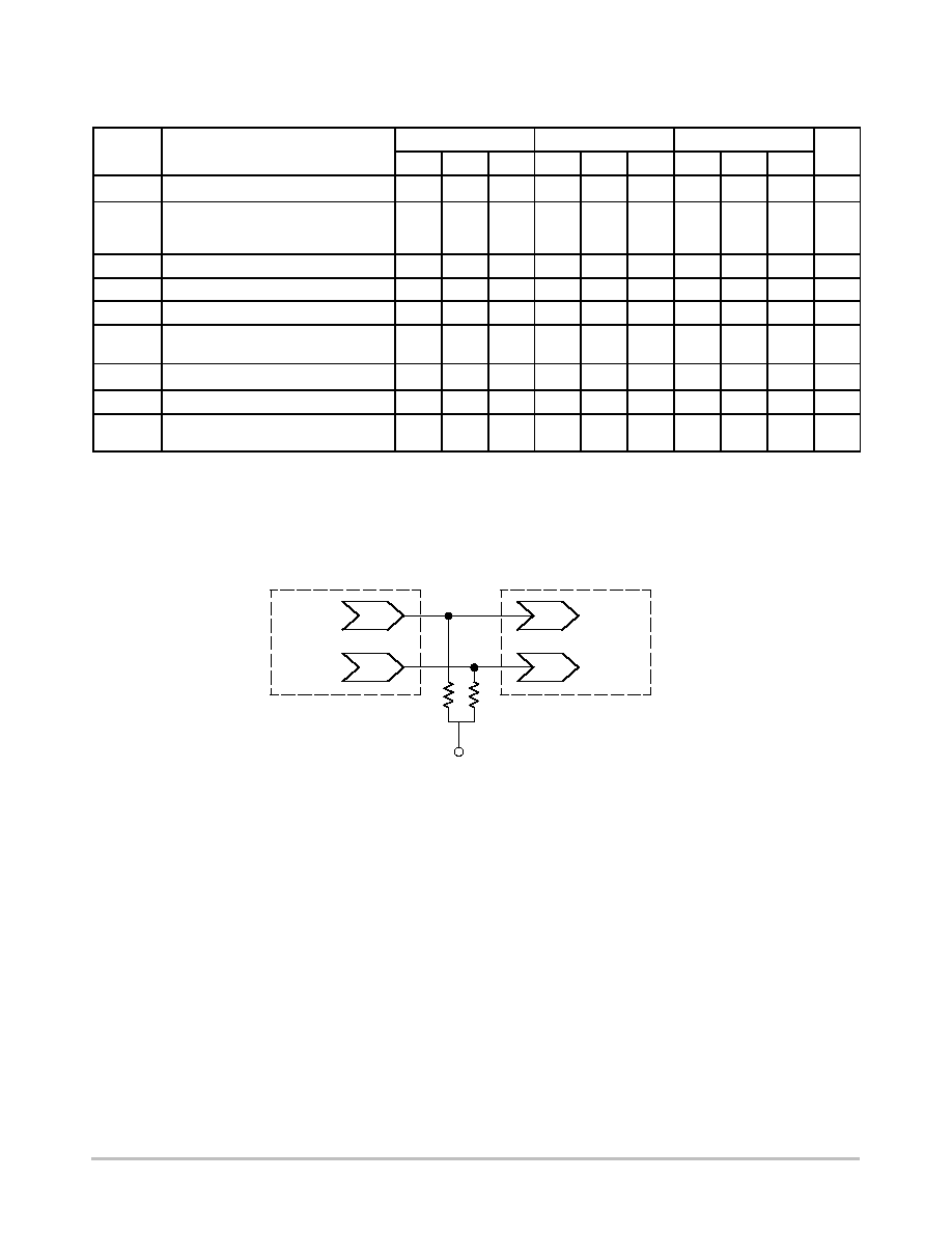
V TT = V CC ≠ 2.0 V
Figure 1. Typical Termination for Output Driver and Device Evaluation
(See Application Note AND8020 ≠ Termination of ECL Logic Devices.)
W
Driver
Device
Receiver
Device
Q
Qb
D
Db
50
W
50
V TT

MC100LVEL51
http://onsemi.com
5
Resource Reference of Application Notes
AN1404
≠
ECLinPS Circuit Performance at Non≠Standard V
IH
Levels
AN1405
≠
ECL Clock Distribution Techniques
AN1406
≠
Designing with PECL (ECL at +5.0 V)
AN1503
≠
ECLinPS I/O SPICE Modeling Kit
AN1504
≠
Metastability and the ECLinPS Family
AN1560
≠
Low Voltage ECLinPS SPICE Modeling Kit
AN1568
≠
Interfacing Between LVDS and ECL
AN1596
≠
ECLinPS Lite Translator ELT Family SPICE I/O Model Kit
AN1650
≠
Using Wire≠OR Ties in ECLinPS Designs
AN1672
≠
The ECL Translator Guide
AND8001
≠
Odd Number Counters Design
AND8002
≠
Marking and Date Codes
AND8020
≠
Termination of ECL Logic Devices