 | –≠–ª–µ–∫—Ç—Ä–æ–Ω–Ω—ã–π –∫–æ–º–ø–æ–Ω–µ–Ω—Ç: MC10EP142 | –°–∫–∞—á–∞—Ç—å:  PDF PDF  ZIP ZIP |
©
Semiconductor Components Industries, LLC, 2003
March, 2003 - Rev. 9
1
Publication Order Number:
MC10EP142/D
MC10EP142, MC100EP142
3.3V / 5V ECL 9-Bit Shift
Register
The MC10EP/100EP142 is a 9-bit shift register, designed with
byte-parity applications in mind. The MC10/100EP142 is capable of
performing serial/parallel data into serial/parallel out and shifting in
only one direction. The nine inputs D0 - D8 accept parallel input data,
while S-IN accepts serial input data. The QT0:87 outputs do not need
to be terminated for the shift operation to function. To minimize
power, any Q output not used should be left unterminated.
The SEL (Select) input pin is used to switch between the two modes
of operation - SHIFT and LOAD. The shift direction is from bit 0 to
bit 8. Input data is accepted by the registers a set-up time before the
positive going edge of CLK0 or CLK1; shifting is also accomplished
on the positive clock edge. A HIGH on the Master Reset pin (MR)
asynchronously resets all the resisters to zero.
The 100 Series contains temperature compensation.
∑
Minimum Shift Frequency >3 GHz (Typical)
∑
9-Bit for Byte-Parity Applications
∑
Asynchronous Master Reset
∑
Dual Clocks
∑
PECL Mode Operating Range: V
CC
= 3.0 V to 5.5 V
with V
EE
= 0 V
∑
NECL Mode Operating Range: V
CC
= 0 V
with V
EE
= -3.0 V to -5.5 V
∑
Open Input Default State
∑
Safety Clamp on Inputs
Device
Package
Shipping
ORDERING INFORMATION
MC10EP142FA
LQFP-32
250 Units/Tray
MC10EP142FAR2
LQFP-32
2000/Tape & Reel
LQFP-32
FA SUFFIX
CASE 873A
MARKING
DIAGRAM*
MCxxx
AWLYYWW
xxx = 10 or 100
A
= Assembly Location
WL = Wafer Lot
YY
= Year
WW = Work Week
*For additional information, refer to Application Note
AND8002/D
EP142
MC100EP142FA
LQFP-32
250 Units/Tray
MC100EP142FAR2
LQFP-32
2000/Tape & Reel
1
32
http://onsemi.com

MC10EP142, MC100EP142
http://onsemi.com
2
Figure 1. 32-Lead LQFP Pinout (Top View)
25
26
27
28
29
30
31
32
15
14
13
12
11
10
9
1
2
3
4
5
6
7
8
24 23 22 21 20 19 18 17
16
D7
D8
Q7
Q4
Q2
V
CC
MR
Q0
CLK0
D6
Q3
Q1
V
EE
SEL
CLK0
CLK1
CLK1
V
CC
S-IN
MC10EP142
MC100EP142
S-IN
V
EE
D0
D1
D2
D3
Q8
Q7
Q6
V
CC
Q5
D4
D5
Table 1. Pin Description
Pin
Name
I/O
Default State
Description
1,23,24,25,26,
27,29,30,31
D[0:8]
ECL Input
Low
Single-Ended Parallel Data Inputs [0:8]. Internal 75 k
W
to V
EE
.
2
S-IN
ECL Input
Low
Noninverted Differential Serial Input. Internal 75 k
W
to V
EE
.
3
S-IN
ECL Input
High
Inverted Differential Serial Input. Internal 75 k
W
to V
EE
and 36.5 k
W
to
V
CC
.
4
CLK0
ECL Input
Low
Noninverted Differential CLK0 Input. Internal 75 k
W
to V
EE
.
5
CLK0
ECL Input
High
Inverted Differential CLK0B Input. Internal 75 k
W
to V
EE
and 36.5 k
W
to V
CC
.
6
CLK1
ECL Input
Low
Noninverted Differential CLK1 Input. Internal 75 k
W
to V
EE
.
7
CLK1
ECL Input
High
Inverted Differential CLK1B Input. Internal 75 k
W
to V
EE
and 36.5 k
W
to V
CC
.
8
SEL
ECL Input
Low
Single-Ended Select Logic Input. Internal 75 k
W
to V
EE
.
9
MR
ECL Input
Low
Single-Ended Master Reset Logic Input. Internal 75 k
W
to V
EE
.
10,11,12,14,1
5,18,19,22
Q0,Q1,Q2,Q3,
Q4,Q5,Q6,Q8
ECL Output
-
Single-Ended parallel Data outputs [0,1,2,3,4,5,6,8]. Typically Termi-
nated with 50
W
to V
TT
= V
CC
- 2 V.
13,17,32
V
CC
-
-
Positive supply Voltage. All V
CC
Pins must be Externally Connected to
Power Supply to Guarantee Proper Operation.
16,28
V
EE
-
-
Negative supply Voltage. All V
EE
Pins must be Externally connected
to Power Supply to Guarantee Proper Operation.
20
Q7
ECL Output
-
Noninverted Differential parallel/Serial Data Output 7. Typically Termi-
nated with 50
W
to V
TT
= V
CC
- 2 V.
21
Q7
ECL Output
-
Inverted Differential parallel/Serial Data Output 7. Typically Termi-
nated with 50
W
to V
TT
= V
CC
- 2 V.
1. All V
CC
and V
EE
pins must be externally connected to Power Supply to guarantee proper operation.

MC10EP142, MC100EP142
http://onsemi.com
3
Table 2. TRUTH TABLE
Function
(Note 2)
SEL
S-IN
MR
CLK0
CLK1
Q0
Q1
Q2
Q3
Q4
Q5
Q6
Q7
Q8
Q9
Load
L
X
L
Z
Z
D0
D1
D2
D3
D4
D5
D6
D7
D8
D9
Shift
H
L
L
Z
Z
L
Q0
Q1
Q2
Q3
Q4
Q5
Q6
Q7
Q8
H
H
L
Z
Z
H
Q0
Q1
Q2
Q3
Q4
Q5
Q6
Q7
Q8
Reset
X
X
H
Z
Z
L
L
L
L
L
L
L
L
L
L
2. All functions are accomplished on the positive edge of CLK0 or CLK1.
MC10EP142, MC100EP142
http://onsemi.com
4
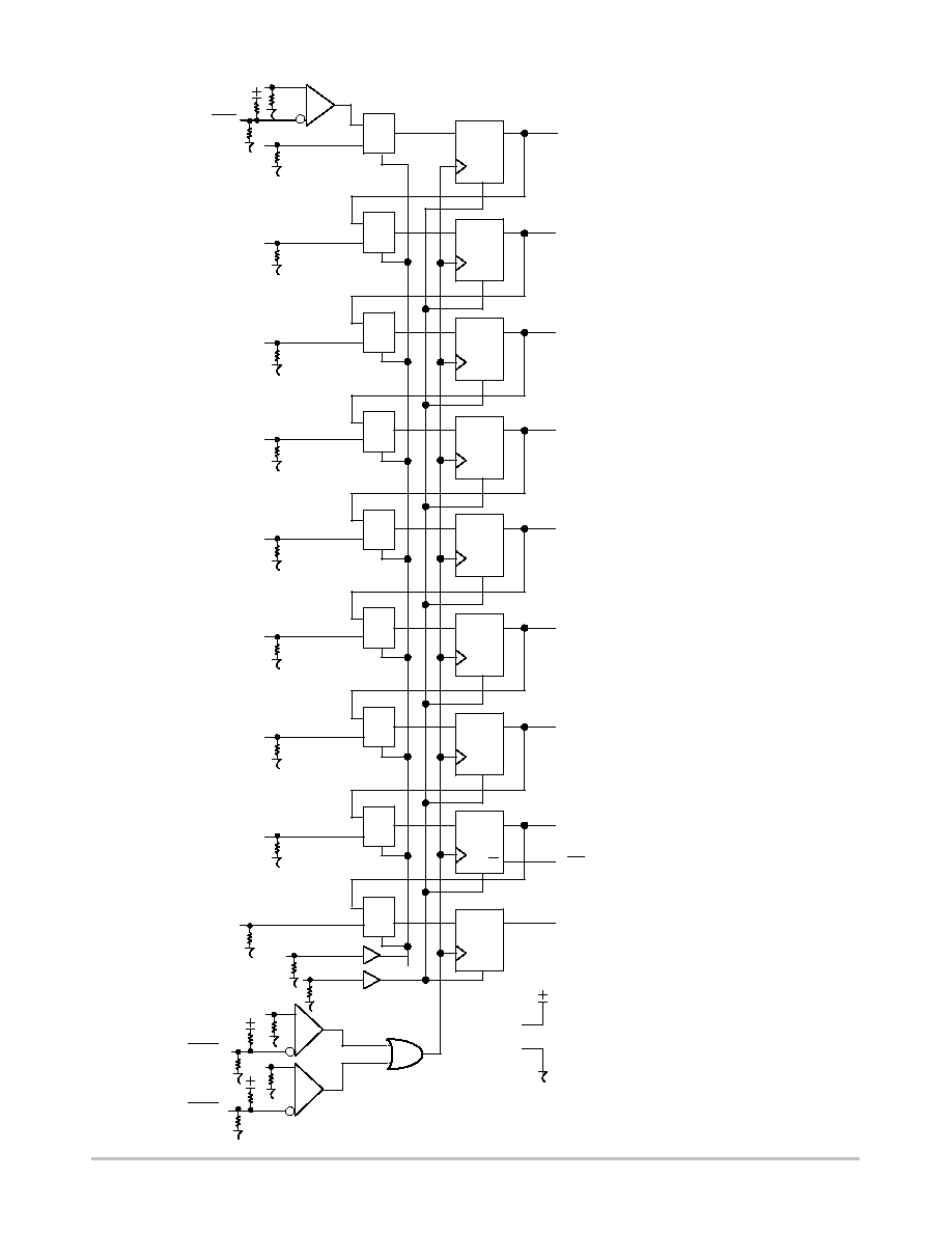
S-IN
D0
D1
S-IN
1
0
D
Q
D
Q
1
0
D2
D3
1
0
1
0
D
Q
D4
D
Q
1
0
D5
1
0
D
Q
1
0
D6
D
Q
1
0
D7
D
Q
1
0
D8
D
Q
D
Q
SEL
MR
CLK0
CLK0
CLK1
CLK1
Q0
Q1
Q2
Q3
Q4
Q5
Q6
Q7
Q7
Q8
Figure 2. Logic Diagram
Q
V
CC
V
EE
R1
R1
R1
R1
R1
R1
R1
R1
R1
R1
R1
R1
R1
R1
R1
R2
R1
R2
R2
R1
MC10EP142, MC100EP142
http://onsemi.com
5
Table 3. ATTRIBUTES
Characteristics
Value
Internal Input Pulldown Resistor
(R1)
75 k
W
Internal Input Pullup Resistor
(R2)
37.5 k
W
ESD Protection
Human Body Model
Machine Model
Charged Device Model
> 2 kV
> 100 V
> 2 kV
Moisture Sensitivity (Note 3)
Level 2
Flammability Rating
Oxygen Index: 28 to 34
UL-94 V-0 @ 0.125 in
Transistor Count
405 Devices
Meets or exceeds JEDEC Spec EIA/JESD78 IC Latchup Test
3. For additional information, refer to Application Note AND8003/D.
Table 4. MAXIMUM RATINGS
(Note 4)
Symbol
Parameter
Condition 1
Condition 2
Rating
Units
V
CC
Positive Power Supply
V
EE
= 0 V
8
V
V
EE
Negative Power Supply
V
CC
= 0 V
-8
V
V
I
PECL Mode Input Voltage
V
EE
= 0 V
V
I
V
CC
6
V
V
I
PECL Mode In ut Voltage
NECL Mode Input Voltage
V
EE
0 V
V
CC
= 0 V
V
I
V
CC
V
I
V
EE
6
-6
V
V
I
out
Output Current
Continuous
Surge
50
100
mA
mA
T
A
Operating Temperature Range
-40 to +85
∞
C
T
stg
Storage Temperature Range
-65 to +150
∞
C
q
JA
Thermal Resistance (Junction-to-Ambient)
0 LFPM
500 LFPM
32 LQFP
32 LQFP
80
55
∞
C/W
∞
C/W
q
JC
Thermal Resistance (Junction-to-Case)
std bd
32 LQFP
12 to 17
∞
C/W
T
sol
Wave Solder
<2 to 3 sec @ 248
∞
C
265
∞
C
4. Maximum Ratings are those values beyond which device damage may occur.
Table 5. 10EP DC CHARACTERISTICS, PECL
V
CC
= 3.3 V, V
EE
= 0 V (Note 5)
-40
∞
C
25
∞
C
85
∞
C
Symbol
Characteristic
Min
Typ
Max
Min
Typ
Max
Min
Typ
Max
Unit
I
EE
Negative Power Supply Current
105
125
145
105
125
145
105
125
145
mA
V
OH
Output HIGH Voltage (Note 6)
2165
2290
2415
2230
2355
2480
2290
2415
2540
mV
V
OL
Output LOW Voltage (Note 6)
1365
1490
1615
1430
1555
1680
1490
1615
1740
mV
V
IH
Input HIGH Voltage (Single-Ended)
2090
2415
2155
2480
2215
2540
mV
V
IL
Input LOW Voltage (Single-Ended)
1365
1690
1460
1755
1490
1815
mV
V
IHCMR
Input HIGH Voltage Common Mode
Range (Differential Configuration)
(Note 7)
2.0
3.3
2.0
3.3
2.0
3.3
V
I
IH
Input HIGH Current (@ V
IH
)
150
150
150
m
A
I
IL
Input LOW Current (@ V
IL
)
CLK0, CLK1, D, S-IN
CLK0, CLK1, D, S-IN
0.5
-150
0.5
-150
0.5
-150
m
A
NOTE: EP circuits are designed to meet the DC specifications shown in the above table after thermal equilibrium has been established. The
circuit is in a test socket or mounted on a printed circuit board and transverse airflow greater than 500 lfpm is maintained.
5. Input and output parameters vary 1:1 with V
CC
. V
EE
can vary +0.3 V to -2.2 V.
6. All loading with 50
W
to V
CC
-2.0 V.
7. V
IHCMR
min varies 1:1 with V
EE
, V
IHCMR
max varies 1:1 with V
CC
. The V
IHCMR
range is referenced to the most positive side of the differential
input signal.