©
Semiconductor Components Industries, LLC, 2004
June, 2004 - Rev. 5
1
Publication Order Number:
MC10EP446/D
MC10EP446, MC100EP446
3.3V/5V 8-Bit
CMOS/ECL/TTL Data Input
Parallel/Serial Converter
The MC10/100EP446 is an integrated 8-bit parallel to serial data
converter. The device is designed with unique circuit topology to
operate for NRZ data rates up to 3.2 Gb/s. The conversion sequence
from parallel data into a serial data stream is from bit D0 to D7. The
parallel input pins D0-D7 are configurable to be threshold controlled by
CMOS, ECL, or TTL level signals. The serial data rate output can be
selected at internal clock data rate or twice the internal clock data rate
using the CKSEL pin.
Control pins are provided to reset (SYNC) and disable internal clock
circuitry (CKEN). In either CKSEL modes, the internal flip-flops are
triggered on the rising edge for CLK and the multiplexers are switched
on the falling edge of CLK, therefore, all associated specification
limits are referenced to the negative edge of the clock input.
Additionally, V
BB
pin is provided for single-ended input condition.
The 100 Series devices contain temperature compensation network.
∑
3.2 Gb/s Typical Data Rate Capability
∑
Differential Clock and Serial Outputs
∑
V
BB
Output for Single-ended Input Applications
∑
Asynchronous Data Reset (SYNC)
∑
PECL Mode Operating Range:
V
CC
= 3.0 V to 5.5 V with V
EE
= 0 V
∑
NECL Mode Operating Range:
V
CC
= 0 V with V
EE
= -3.0 V to -5.5 V
∑
Open Input Default State
∑
Safety Clamp on Inputs
∑
Parallel Interface Can Support PECL, TTL or CMOS
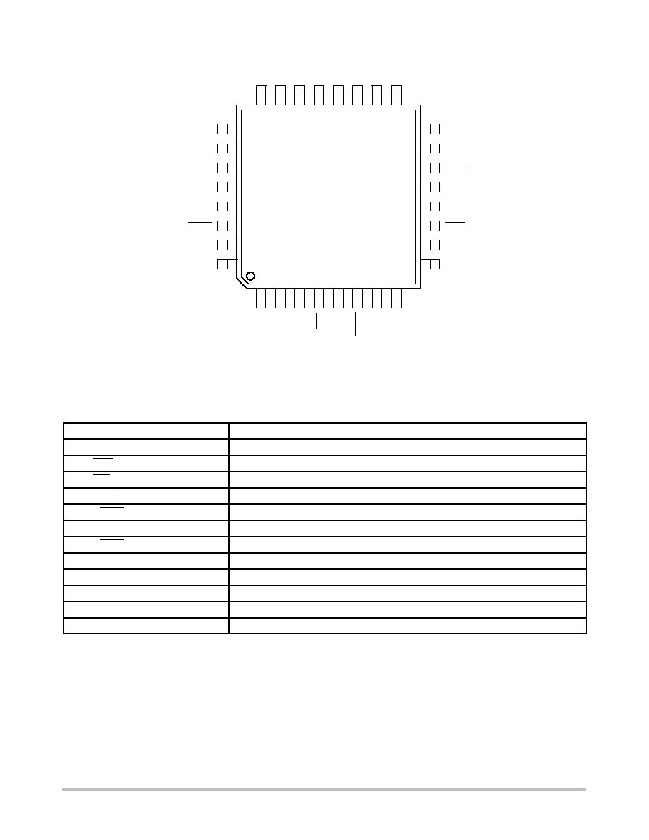
LQFP-32
FA SUFFIX
CASE 873A
MARKING DIAGRAM*
MCXXX
AWLYYWW
XXX
= 10 or 100
A
= Assembly Location
WL
= Wafer Lot
YY
= Year
WW
= Work Week
EP446
*For additional marking information, refer to
Application Note AND8002/D.
32
1
http://onsemi.com
See detailed ordering and shipping information in the package
dimensions section on page 17 of this data sheet.
ORDERING INFORMATION
MC10EP446, MC100EP446
http://onsemi.com
2
25
26
27
28
29
30
31
32
15
14
13
12
11
10
9
1
2
3
4
5
6
7
8
24
23
22
21
20
19
18
17
16
Figure 1. LQFP-32 Pinout (Top View)
Warning: All V
CC
and V
EE
pins must be externally connected
to Power Supply to guarantee proper operation.
D0
D1
D3
D4
D7
V
CC
S
OUT
V
EE
V
BB2
V
CC
CKSEL
V
EF
V
EE
PCLK
PCLK
D2
D5
D6
S
OUT
V
CF
SYNC
SYNC
V
CC
CLK
CLK
V
BB1
CKEN
CKEN
V
EE
V
CC
V
CC
V
CC
MC10EP446
MC100EP446
Table 1. PIN DESCRIPTION
PIN
FUNCTION
D0*-D7*
ECL, CMOS, or TTL Parallel Data Input
S
OUT
, S
OUT
ECL Differential Serial Data Output
CLK*, CLK*
ECL Differential Clock Input
PCLK, PCLK
ECL Differential Parallel Clock Output
SYNC*, SYNC**
ECL Conversion Synchronizing Differential Input (Reset)***
CKSEL*
ECL Clock Input Selector
CKEN*, CKEN*
ECL Clock Enable Differential Input
V
CF
ECL, CMOS, or TTL Input Selector
V
EF
ECL Reference Mode Connection
V
BB1
,
V
BB2
Reference Voltage Output
V
CC
Positive Supply
V
EE
Negative Supply
* Pins will default LOW when left open.
**Pins will default HIGH when left open.
***The rising edge of SYNC will asynchronously reset the internal circuitry. The falling edge of the SYNC followed by the falling edge of CLK
initiates the conversion process synchronously on the next rising edge of CLK.

MC10EP446, MC100EP446
http://onsemi.com
3
Table 2. TRUTH TABLE
Function
Pin
HIGH
LOW
CKSEL
S
OUT
: PCLK = 8:1
CLK: S
OUT
= 1:1
S
OUT
CLK
S
OUT
: PCLK = 8:1
CLK: S
OUT
= 1:2
S
OUT
CLK
CKEN
Synchronously Disables Normal Parallel to Serial Con-
version
Synchronously Enables Normal Parallel to Serial Conversion
SYNC
Asynchronously Resets Internal Flip-Flops*
Synchronous Enable
*The rising edge of SYNC will asynchronously reset the internal circuitry. The falling edge of the SYNC followed by the falling edge of CLK initiates
the conversion process synchronously on the next rising edge of CLK.
Table 3. INPUT VOLTAGE LEVEL SELECTION TABLE
Input Function
Connect To V
CF
Pin
ECL Mode
V
EF
Pin
CMOS Mode
No Connect
TTL Mode*
1.5 V
$
100 mV
*For TTL Mode, if no external voltage can be provided, the reference
voltage can be provided by connecting the appropriate resistor
between V
CF
and V
EE
pins.
Table 4. DATA INPUT OPERATING VOLTAGE TABLE
Power Supply
Data Inputs (D [0:7])
Power Supply
(V
CC
,V
EE
)
CMOS
TTL
PECL
NECL
PECL
p
p
p
N/A
NECL
N/A
N/A
N/A
p
Power Supply
Resistor Value 10% (Tolerance)
3.3 V
1.5 k
W
5.0 V
500
W

MC10EP446, MC100EP446
http://onsemi.com
4
SYNC
Figure 2. Logic Diagram
D0
D
Q
R
C
D
Q
R
C
D4
D
Q
R
C
D
Q
R
C
D
Q
R
C
D
Q
R
C
D
Q
R
C
D
Q
R
C
D2
D6
D1
D5
D3
D7
MUX
2:1
MUX
2:1
MUX
2:1
MUX
2:1
D
Q
R
C
D
Q
R
C
D
Q
R
C
D
Q
R
C
˜
2
MUX
2:1
MUX
2:1
D
Q
R
C
D
Q
R
C
MUX
2:1
˜
2
˜
2
D
Q
R
C
S
OUT
S
OUT
PCLK
PCLK
MUX
2:1
CKEN
CKEN
CLK
CLK
CKSEL
SYNC
V
BB
V
CF
V
EF
V
EE
Control
Logic
V
CC
MC10EP446, MC100EP446
http://onsemi.com
5
Table 5. ATTRIBUTES
Characteristics
Value
Internal Input Pulldown Resistor
75 k
W
Internal Input Pullup Resistor
37.5 k
W
ESD Protection
Human Body Model
Machine Model
Charged Device Model
> 2 kV
> 100 V
> 2 kV
Moisture Sensitivity (Note 1)
Level 2
Flammability Rating
Oxygen Index: 28 to 34
UL 94 V-0 @ 0.125 in
Transistor Count
962 Devices
Meets or exceeds JEDEC Spec EIA/JESD78 IC Latchup Test
1. For additional information, see Application Note AND8003/D.
Table 6. MAXIMUM RATINGS
Symbol
Parameter
Condition 1
Condition 2
Rating
Unit
V
CC
PECL Mode Power Supply
V
EE
= 0 V
6
V
V
EE
NECL Mode Power Supply
V
CC
= 0 V
-6
V
V
I
PECL Mode Input Voltage
NECL Mode Input Voltage
V
EE
= 0 V
V
CC
= 0 V
V
I
V
CC
V
I
V
EE
6
-6
V
V
I
out
Output Current
Continuous
Surge
50
100
mA
mA
I
BB
V
BB
Sink/Source
±
0.5
mA
T
A
Operating Temperature Range
-40 to +85
∞
C
T
stg
Storage Temperature Range
-65 to +150
∞
C
q
JA
Thermal Resistance (Junction-to-Ambient)
0 lfpm
500 lfpm
LQFP-32
LQFP-32
80
55
∞
C/W
∞
C/W
q
JC
Thermal Resistance (Junction-to-Case)
Standard Board
LQFP-32
12 to 17
∞
C/W
T
sol
Wave Solder
< 2 to 3 sec @ 248
∞
C
265
∞
C
Maximum ratings are those values beyond which device damage can occur. Maximum ratings applied to the device are individual stress limit
values (not normal operating conditions) and are not valid simultaneously. If these limits are exceeded, device functional operation is not implied,
damage may occur and reliability may be affected.